For free samples & the latest literature: http://www.maxim-ic.com, or phone 1-800-998-8800.
For small orders, phone 1-800-835-8769.
General Description
The MAX3120 IrDA 1.2-compatible infrared transceiver
is optimized for battery-powered, space-constrained
applications. It consumes only 120µA while supporting
data rates up to 115kbps over a wide 3V to 5.5V operating range, and features a 10nA shutdown mode to
further extend battery life.
The MAX3120 reduces the space required for IrDA
applications by requiring a minimum of external components: photodiode, infrared LED, and current-setting
resistor. Optical components are external to allow maximum flexibility in PC board design. The MAX3120 is
available in 8-pin µMAX and SO packages. The µMAX
package consumes half the board space of an 8-pin
SO.
Applications
IrDA Applications
Personal Digital Assistants (PDAs)
Palmtop Computers
Cell Phones
Hand-Held Equipment
Peripherals
Features
♦ IrDA 1.2 Compatible: 2.4kbps to 115.2kbps
♦ +3V to +5.5V Single-Supply Operation
♦ Flexible Optics Selection and Layout
♦ 120µA Supply Current
♦ 10nA Shutdown Supply Current
♦ 200mA, High-Current Infrared LED Drive
MAX3120
Low-Profile, 3V, 120µA,
IrDA Infrared Transceiver
________________________________________________________________
Maxim Integrated Products
1
1
2
3
4
8
7
6
5
RXD
LEDC
PGND
SHDNPINC
GND
V
CC
TXD
MAX3120
µMAX/SO
TOP VIEW
19-1390; Rev 0; 10/98
PART
MAX3120CUA
MAX3120CSA
MAX3120EUA -40°C to +85°C
0°C to +70°C
0°C to +70°C
TEMP. RANGE PIN-PACKAGE
8 µMAX
8 SO
8 µMAX
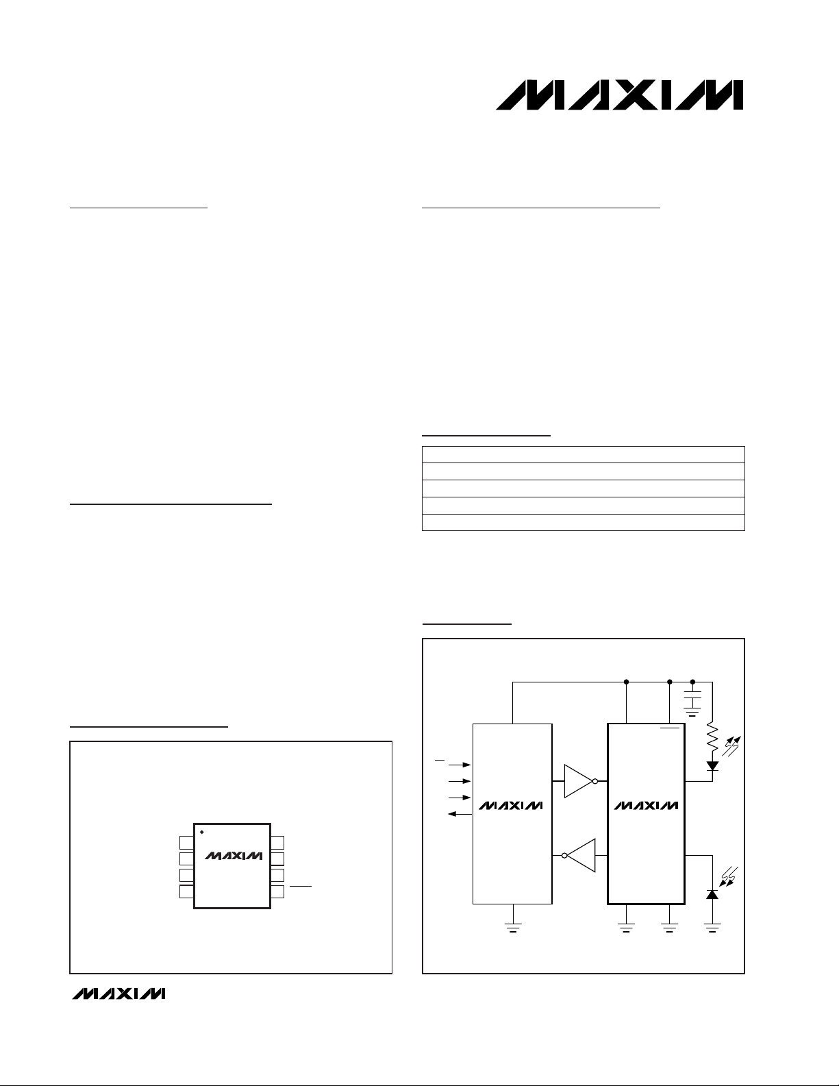
Pin Configuration
Ordering Information
MAX3120ESA -40°C to +85°C 8 SO
MAX3120
RXD PINC
LEDC
TXD
+3.3V
V
CC
SHDN
GND PGND
MAX3100
CS
SCLK
DIN
DOUT
RX
TX
V
CC
GND
PIN
DIODE
LED
Typical Operating Circuit

MAX3120
Low-Profile, 3V, 120µA,
IrDA Infrared Transceiver
2 _______________________________________________________________________________________
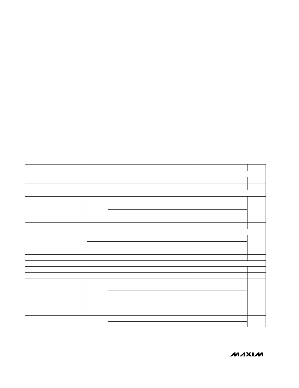
ABSOLUTE MAXIMUM RATINGS
ELECTRICAL CHARACTERISTICS
(VCC= +3.0V to +5.5V, TA= T
MIN
to T
MAX
, unless otherwise noted. Typical values are at TA= +25°C and VCC= +3.3V.)
Stresses beyond those listed under “Absolute Maximum Ratings” may cause permanent damage to the device. These are stress ratings only, and functional
operation of the device at these or any other conditions beyond those indicated in the operational sections of the specifications is not implied. Exposure to
absolute maximum rating conditions for extended periods may affect device reliability.
(Referred to GND)
V
CC
...........................................................................-0.3V to +6V
TXD,
SHDN, LEDC ...................................................-0.3V to +6V
RXD ............................................................-0.3V to (V
CC
+ 0.3V)
PGND ....................................................................-0.1V to +0.1V
PINC....................................................................................10mA
Continuous LEDC Current.................................................200mA
Repetitive Pulsed LEDC Current
(<90µs, duty cycle <20%) ..........................................500mA
Continuous Power Dissipation (T
A
= +70°C)
µMAX (derate 4.1mW/°C above +70°C)....................330mW
SO (derate 5.88mW/°C above +70°C).......................471mW
Operating Temperature Ranges
MAX3120C_A....................................................0°C to +70°C
MAX3120E_A.................................................-40°C to +85°C
Junction Temperature......................................................+150°C
Storage Temperature Range.............................-65°C to +160°C
Lead Temperature (soldering, 10sec).............................+300°C
Data rate = 2.4kbps
TA= +25°C, SHDN = GND (Note 1)
Delay until maximum IR receiver data rate is
valid
Delay until ICC< 1µA
TA= +25°C, SHDN = VCC(Note 1)
VCC= 5.0V
VCC= 3.3V
(Note 3)
(Note 2)
I
SINK
= 200µA
VCC= 3.3V
C
LOAD
= 50pF
VCC= 5.0V
I
SOURCE
= 100µA
CONDITIONS
µs
190
IR Receiver Output Pulse Width
µs300Shutdown Disable Time
µs10Shutdown Time
375
µA
100
Ambient DC Current Rejection
mA0.0002 6Input Current Sensitivity
nA
RMS
10I
NOISE
Equivalent Input Noise Current
kbps2.4 115.2Supported Data Rates
ns50tr, t
f
Output Rise and Fall Time
V
CC
-V
CC
-
0.5 0.05
V
OH
µA0.01 1.0I
CC(SHDN)
Shutdown Supply Current
µA120 200I
CC
Supply Current
V
0.1 0.4V
OL
Output Voltage
pF2C
IN
Input Capacitance
µA-1 1I
LEAK
Input Leakage Current
V0.8V
IL
Input Logic Threshold Low
V
2.0
V
IH
Input Logic Threshold High
2.4
UNITSMIN TYP MAXSYMBOLPARAMETER
Data rate = 115.2kbps 18
DC CHARACTERISTICS
LOGIC OUTPUT (RXD)
LOGIC INPUTS (TXD, SHDN)
IR RECEIVER

MAX3120
Low-Profile, 3V, 120µA,
IrDA Infrared Transceiver
_______________________________________________________________________________________
3
0.6
0.8
1.2
1.0
1.4
1.6
-40 10-15 35 60 85
LED DRIVER
ON-RESISTANCE vs. TEMPERATURE
MAX3120 TOC01
TEMPERATURE (°C)
R
LEDC
(Ω)
I
LEDC
= 100mA
VCC = 3.3V
VCC = 5V
90
100
120
110
130
140
-40 10-15 35 60 85
SUPPLY CURRENT
vs. TEMPERATURE
MAX3120 TOC02
TEMPERATURE (°C)
SUPPLY CURRENT
(µA)
VCC = 3V
VCC = 5V
105
115
110
125
120
130
135
3.0 4.03.5 4.5 5.0 5.5
SUPPLY CURRENT
vs. SUPPLY VOLTAGE
MAX3120 TOC03
SUPPLY VOLTAGE (V)
SUPPLY CURRENT
(µA)
0
200
100
400
300
500
600
100 250 300150 200 350 400
LEDC VOLTAGE
vs. LEDC CURRENT
MAX3120 toc04
LEDC CURRENT (mA)
V
LEDC
(mV)
VCC = 3.3V
VCC = 5V
PULSED AT
20% DUTY CYCLE
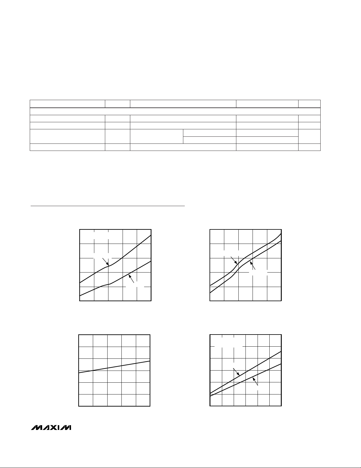
Typical Operating Characteristics
(TA = +25°C, unless otherwise noted.)
CONDITIONS UNITSMIN TYP MAXSYMBOLPARAMETER
Transmitter Rise Time t
r
10% to 90% of 200mA drive current 20 600 ns
Transmitter Fall Time t
f
90% to 10% of 200mA drive current 20 600 ns
Transmitter Output Resistance I
OUT
= 200mA
1.15 2.0
Ω
0.9 1.6
Off-Leakage Current 0.01 10 µA
VCC= 5.0V
VCC= 3.3V
IR TRANSMITTER
Note 1: All supply current measurements are made under the following conditions: no load at all outputs, input voltages at GND or
V
CC
, no PIN diode input current.
Note 2: Equivalent input current noise is calculated by dividing the output noise of the transimpedance amplifier by the midband
transimpedance gain.
Note 3: Sensitivity is measured with an IrDA-compliant input signal, where the data rate is within the Supported Data Rate, rise/fall
times are less than 600ns, and pulse widths are between 1.41µs and 3/16 of the baud rate.
ELECTRICAL CHARACTERISTICS (continued)
(VCC= +3.0V to +5.5V, TA= T
MIN
to T
MAX
, unless otherwise noted. Typical values are at TA= +25°C and VCC= +3.3V.)
 Loading...