

Page 1
For free samples & the latest literature: http://www.maxim-ic.com, or phone 1-800-998-8800.
For small orders, phone 1-800-835-8769.
General Description
The MAX3120 IrDA 1.2-compatible infrared transceiver
is optimized for battery-powered, space-constrained
applications. It consumes only 120µA while supporting
data rates up to 115kbps over a wide 3V to 5.5V operating range, and features a 10nA shutdown mode to
further extend battery life.
The MAX3120 reduces the space required for IrDA
applications by requiring a minimum of external components: photodiode, infrared LED, and current-setting
resistor. Optical components are external to allow maximum flexibility in PC board design. The MAX3120 is
available in 8-pin µMAX and SO packages. The µMAX
package consumes half the board space of an 8-pin
SO.
Applications
IrDA Applications
Personal Digital Assistants (PDAs)
Palmtop Computers
Cell Phones
Hand-Held Equipment
Peripherals
Features
♦ IrDA 1.2 Compatible: 2.4kbps to 115.2kbps
♦ +3V to +5.5V Single-Supply Operation
♦ Flexible Optics Selection and Layout
♦ 120µA Supply Current
♦ 10nA Shutdown Supply Current
♦ 200mA, High-Current Infrared LED Drive
MAX3120
Low-Profile, 3V, 120µA,
IrDA Infrared Transceiver
________________________________________________________________
Maxim Integrated Products
1
1
2
3
4
8
7
6
5
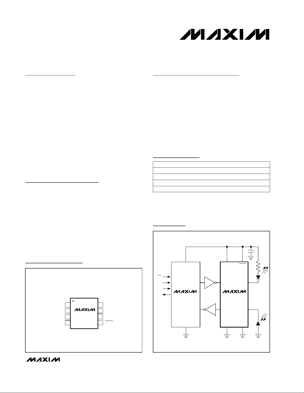
RXD
LEDC
PGND
SHDNPINC
GND
V
CC
TXD
MAX3120
µMAX/SO
TOP VIEW
19-1390; Rev 0; 10/98
PART
MAX3120CUA
MAX3120CSA
MAX3120EUA -40°C to +85°C
0°C to +70°C
0°C to +70°C
TEMP. RANGE PIN-PACKAGE
8 µMAX
8 SO
8 µMAX
Pin Configuration
Ordering Information
MAX3120ESA -40°C to +85°C 8 SO
MAX3120
RXD PINC
LEDC
TXD
+3.3V
V
CC
SHDN
GND PGND
MAX3100
CS
SCLK
DIN
DOUT
RX
TX
V
CC
GND
PIN
DIODE
LED
Typical Operating Circuit
Page 2
MAX3120
Low-Profile, 3V, 120µA,
IrDA Infrared Transceiver
2 _______________________________________________________________________________________
ABSOLUTE MAXIMUM RATINGS
ELECTRICAL CHARACTERISTICS
(VCC= +3.0V to +5.5V, TA= T
MIN
to T
MAX
, unless otherwise noted. Typical values are at TA= +25°C and VCC= +3.3V.)
Stresses beyond those listed under “Absolute Maximum Ratings” may cause permanent damage to the device. These are stress ratings only, and functional
operation of the device at these or any other conditions beyond those indicated in the operational sections of the specifications is not implied. Exposure to
absolute maximum rating conditions for extended periods may affect device reliability.
(Referred to GND)
V
CC
...........................................................................-0.3V to +6V
TXD,
SHDN, LEDC ...................................................-0.3V to +6V
RXD ............................................................-0.3V to (V
CC
+ 0.3V)
PGND ....................................................................-0.1V to +0.1V
PINC....................................................................................10mA
Continuous LEDC Current.................................................200mA
Repetitive Pulsed LEDC Current
(<90µs, duty cycle <20%) ..........................................500mA
Continuous Power Dissipation (T
A
= +70°C)
µMAX (derate 4.1mW/°C above +70°C)....................330mW
SO (derate 5.88mW/°C above +70°C).......................471mW
Operating Temperature Ranges
MAX3120C_A....................................................0°C to +70°C
MAX3120E_A.................................................-40°C to +85°C
Junction Temperature......................................................+150°C
Storage Temperature Range.............................-65°C to +160°C
Lead Temperature (soldering, 10sec).............................+300°C
Data rate = 2.4kbps
TA= +25°C, SHDN = GND (Note 1)
Delay until maximum IR receiver data rate is
valid
Delay until ICC< 1µA
TA= +25°C, SHDN = VCC(Note 1)
VCC= 5.0V
VCC= 3.3V
(Note 3)
(Note 2)
I
SINK
= 200µA
VCC= 3.3V
C
LOAD
= 50pF
VCC= 5.0V
I
SOURCE
= 100µA
CONDITIONS
µs
190
IR Receiver Output Pulse Width
µs300Shutdown Disable Time
µs10Shutdown Time
375
µA
100
Ambient DC Current Rejection
mA0.0002 6Input Current Sensitivity
nA
RMS
10I
NOISE
Equivalent Input Noise Current
kbps2.4 115.2Supported Data Rates
ns50tr, t
f
Output Rise and Fall Time
V
CC
-V
CC
-
0.5 0.05
V
OH
µA0.01 1.0I
CC(SHDN)
Shutdown Supply Current
µA120 200I
CC
Supply Current
V
0.1 0.4V
OL
Output Voltage
pF2C
IN
Input Capacitance
µA-1 1I
LEAK
Input Leakage Current
V0.8V
IL
Input Logic Threshold Low
V
2.0
V
IH
Input Logic Threshold High
2.4
UNITSMIN TYP MAXSYMBOLPARAMETER
Data rate = 115.2kbps 18
DC CHARACTERISTICS
LOGIC OUTPUT (RXD)
LOGIC INPUTS (TXD, SHDN)
IR RECEIVER
Page 3
MAX3120
Low-Profile, 3V, 120µA,
IrDA Infrared Transceiver
_______________________________________________________________________________________
3
0.6
0.8
1.2
1.0
1.4
1.6
-40 10-15 35 60 85
LED DRIVER
ON-RESISTANCE vs. TEMPERATURE
MAX3120 TOC01
TEMPERATURE (°C)
R
LEDC
(Ω)
I
LEDC
= 100mA
VCC = 3.3V
VCC = 5V
90
100
120
110
130
140
-40 10-15 35 60 85
SUPPLY CURRENT
vs. TEMPERATURE
MAX3120 TOC02
TEMPERATURE (°C)
SUPPLY CURRENT
(µA)
VCC = 3V
VCC = 5V
105
115
110
125
120
130
135
3.0 4.03.5 4.5 5.0 5.5
SUPPLY CURRENT
vs. SUPPLY VOLTAGE
MAX3120 TOC03
SUPPLY VOLTAGE (V)
SUPPLY CURRENT
(µA)
0
200
100
400
300
500
600
100 250 300150 200 350 400
LEDC VOLTAGE
vs. LEDC CURRENT
MAX3120 toc04
LEDC CURRENT (mA)
V
LEDC
(mV)
VCC = 3.3V
VCC = 5V
PULSED AT
20% DUTY CYCLE
Typical Operating Characteristics
(TA = +25°C, unless otherwise noted.)
CONDITIONS UNITSMIN TYP MAXSYMBOLPARAMETER
Transmitter Rise Time t
r
10% to 90% of 200mA drive current 20 600 ns
Transmitter Fall Time t
f
90% to 10% of 200mA drive current 20 600 ns
Transmitter Output Resistance I
OUT
= 200mA
1.15 2.0
Ω
0.9 1.6
Off-Leakage Current 0.01 10 µA
VCC= 5.0V
VCC= 3.3V
IR TRANSMITTER
Note 1: All supply current measurements are made under the following conditions: no load at all outputs, input voltages at GND or
V
CC
, no PIN diode input current.
Note 2: Equivalent input current noise is calculated by dividing the output noise of the transimpedance amplifier by the midband
transimpedance gain.
Note 3: Sensitivity is measured with an IrDA-compliant input signal, where the data rate is within the Supported Data Rate, rise/fall
times are less than 600ns, and pulse widths are between 1.41µs and 3/16 of the baud rate.
ELECTRICAL CHARACTERISTICS (continued)
(VCC= +3.0V to +5.5V, TA= T
MIN
to T
MAX
, unless otherwise noted. Typical values are at TA= +25°C and VCC= +3.3V.)
Page 4

MAX3120
Low-Profile, 3V, 120µA,
IrDA Infrared Transceiver
4 _______________________________________________________________________________________
Typical Operating Characteristics (continued)
(TA = +25°C, unless otherwise noted.)
1.0
2.0
1.5
3.0
2.5
3.5
4.0
04020 60 80 100
RXD OUTPUT PULSE WIDTH
vs. DISTANCE
MAX3120 TOC07
DISTANCE (cm)
RXD PULSE WIDTH
(µs)
TRANSMITTER POWER = 200mW/sr
INPUT PULSE WIDTH = 1.63µs
TEMIC BPV22NF
V
CC
= 3.3V
2V/div
2V/div
RXD OUTPUT
vs. INFRARED INPUT
MAX3120 toc11
100µs/div
RXD
OUTPUT
INFRARED
INPUT
V
CC
= 3.3V, 2400bps AT 10cm DISTANCE,
TERMIC BPV22NF, TRANSMIT POWER 200mW/sr
2V/div
2V/div
RXD OUTPUT
vs. INFRARED INPUT
MAX3120 toc09
100µs/div
RXD
OUTPUT
INFRARED
INPUT
V
CC
= 3.3V, 2400bps AT 1cm DISTANCE,
TERMIC BPV22NF, TRANSMIT POWER 200mW/sr
2V/div
2V/div
RXD OUTPUT
vs. INFRARED INPUT
MAX3120 toc10
2µs/div
RXD
OUTPUT
INFRARED
INPUT
V
CC
= 3.3V, 115.2kbps AT 10cm DISTANCE,
TERMIC BPV22NF, TRANSMIT POWER 200mW/sr
2V/div
2V/div
RXD OUTPUT
vs. INFRARED INPUT
MAX3120 toc08
2µs/div
RXD
OUTPUT
INFRARED
INPUT
V
CC
= 3.3V, 115.2kbps AT 1cm DISTANCE,
TERMIC BPV22NF, TRANSMIT POWER 200mW/sr
0
20
60
40
80
100
04020 60 80 100
RXD OUTPUT PULSE WIDTH
vs. DISTANCE
MAX3120 TOC06
DISTANCE (cm)
RXD PULSE WIDTH (µs)
TRANSMITTER POWER = 200mW/sr
INPUT PULSE WIDTH = 78µs
TEMIC BPV22NF
V
CC
= 3.3V
0
100
50
250
200
150
400
350
300
450
3.0 4.03.5 4.5 5.0 5.5
AMBIENT PHOTODIODE CURRENT REJECTION
vs. SUPPLY VOLTAGE
MAX3120 TOC05
SUPPLY VOLTAGE (V)
CURRENT REJECTION (µA)
Page 5

MAX3120
Low-Profile, 3V, 120µA,
IrDA Infrared Transceiver
_______________________________________________________________________________________
5
2V/div
2V/div
RXD OUTPUT
vs. INFRARED INPUT
MAX3120 toc12
2µs/div
RXD
OUTPUT
INFRARED
INPUT
V
CC
= 3.3V, 115.2kbps AT 1m DISTANCE,
TERMIC BPV22NF, TRANSMIT POWER 200mW/sr
2V/div
2V/div
RXD OUTPUT
vs. INFRARED INPUT
MAX3120 toc13
100µs/div
RXD
OUTPUT
INFRARED
INPUT
V
CC
= 3.3V, 2400bps AT 1m DISTANCE,
TERMIC BPV22NF, TRANSMIT POWER 200mW/sr
Typical Operating Characteristics (continued)
(TA = +25°C, unless otherwise noted.)
Pin Description
NAME FUNCTION
1 TXD IR Transmitter TTL/CMOS Data Input. High = LED on.
2 V
CC
Supply Voltage
PIN
3 GND Ground. Connect anode of PIN diode to GND. Connect GND to PGND.
4 PINC PIN Diode Cathode Input. Connect cathode of PIN diode to PINC.
8 RXD IR Receiver TTL/CMOS Data Output. Pulses low for IR input pulse.
7 LEDC LED Driver Output. Connect cathode of IR-emitting LED to LEDC.
6 PGND Power Ground. Ground for IR LED driver. Connect PGND to GND.
5
SHDN
Shutdown Input. Active low.
Detailed Description
The MAX3120 is an IrDA 1.2-compatible infrared (IR)
transceiver. By selecting appropriate external optical
components (see
IR LED and PIN Photodiode Selection
section), the MAX3120 will operate at data rates of
2.4kbps to 115kbps at distances from 1cm to 1m.
Because of its low-noise design, the MAX3120
achieves a bit error rate (BER) below 10-8at maximum
data rates when used with the appropriate external
components. On-chip filtering rejects out-of-band
ambient light signals that would otherwise interfere with
IR communication. Also included in the MAX3120 is
a high-power LED driver capable of sinking 200mA. It
can drive most available IR LEDs at IrDA speeds of
2.4kbps to 115kbps.
Receiver
The MAX3120’s IR receiver amplifier reverse biases the
PIN diode by approximately 1.2V, and the PIN diode
converts pulses of IR light into pulses of current. The
input transimpedance (current-to-voltage) amplifier
then converts these current pulses into voltage pulses
of a useful magnitude. The MAX3120 filters the resulting output voltage pulses to remove low-frequency
ambient light interference and high-frequency circuit
noise. Finally, a high-speed comparator translates
these voltage pulses into usable CMOS output levels
(Figure 1).
Page 6

MAX3120
Transmitter
The MAX3120’s IR transmitter consists of a high-power
MOS switch, capable of quickly switching 200mA with
less than 2Ω of on-resistance. Internal buffering keeps
the input capacitance of the TXD pin extremely low to
ease the input drive requirement. Connect an IR LED in
series with a current-setting resistor to select the appropriate IR output power (see the
Powering the IR LED
section). Note that the transmitter does not have an
automatic shutoff circuit, so pay special attention to component power dissipation in high-duty-cycle transmit
schemes.
Applications Information
IR LED and PIN Photodiode Selection
The IrDA specification calls for an IR transmitter with a
peak wavelength between 850nm and 900nm. Within a
±15° half-cone-angle, the output intensity of the IR LED
must be between 40mW/sr and 500mW/sr. Outside a
±30° half-cone-angle, the output intensity of the IR LED
must fall below 40mW/sr. The optical rise and fall times
of the IR LED must be less than 600ns. Based on these
system requirements, the Hewlett Packard HSDL-4220
or the Temic TSHF5400 IR LEDs are two appropriate
choices.
Appropriate PIN photodiode selection is extremely
important to system performance. The PIN diode must
generate at least 200nA (minimum sensitivity of the
MAX3120) of current when aimed ±15° off-axis with an
incident irradiance of 4µW/cm
2
. Use the following equation to determine if the Temic BPV22NF meets these
requirements:
The first term (4µW/cm
2
) is the minimum guaranteed
irradiance in the ±15° angular range. The second term
(0.075cm2) is the effective sensitive area of the PIN
diode. The factor of 1.8 accounts for the efficiency
increase due to the spherical lens. The first 0.95 factor
normalizes the sensitivity to the 875nm wavelength,
while the second 0.95 factor adjusts for decreased
receiver efficiency at ±15° off-axis. The last term,
0.6A/W, is the sensitivity of the PIN diode. In this example, the Temic BPV22NF is an appropriate selection.
The final important factor in selecting a PIN diode is
effective diode capacitance. It is important to keep this
capacitance below 70pF at 1.2V reverse bias. Higher
input capacitance can compromise system noise performance by increasing the noise gain of the input transimpedance amplifier.
Powering the IR LED
Set the current in the IR LED using an external resistor.
Consult the IR LED manufacturer’s data sheet to select
a forward current that will meet IrDA specifications discussed in the
IR LED and PIN Photodiode Selection
section. Look up the drop across the LED (V
LED
) and
the drop across the MAX3120 LED driver (see
Typical
Operating Characteristics
- V
LEDC
) and choose the cur-
rent-setting resistor based on the following equation:
Using the Hewlett Packard HSDL-4220 IR LED as an
example, VCC= 5V, I
SET
= 100mA, and V
LED
= 1.67V,
therefore:
V
LEDC
= 0.08V
R
SET
= 32.5Ω
R=
V-V -V
I
SET
CC LED LEDC
SET
I
PIN
==(4 W/cm )(0.075cm )(1.8)(0.95) (0.6A/W)
291nA
22 2
µ
Low-Profile, 3V, 120µA,
IrDA Infrared Transceiver
6 _______________________________________________________________________________________
Figure 1. Functional Diagram
MAX3120
BIAS
BANDPASS
FILTER
SHDN V
CC
RXD TXD LEDC
PGND
PINC
1.2V
+
-
GND
Page 7

Power-dissipation requirements of the MAX3120, IR
LED, and R
SET
must be met based on maximum duty
cycle and output current requirements.
MAX3120 Power Dissipation = I
SET
· V
LEDC
· Duty Cycle
IR LED Power Dissipation = I
SET
· V
LED
· Duty Cycle
R
SET
Power Dissipation = I
SET
2
· R
SET
· Duty Cycle
Power-Supply Noise Rejection
Because of the extremely sensitive nature of photodiode amplifiers, it is important to maintain a quiet supply
voltage. Use a separate analog supply voltage where
possible. Place a 1µF ceramic bypass capacitor as
close to the VCCpin as possible. In especially noisy
systems, connect a small (10Ω) resistor in series with
VCC, in addition to the normal bypass capacitor.
Layout Considerations
The MAX3120 requires careful layout techniques to minimize parasitic signal coupling to the PINC input. Keep
the lead length between the photodiode and PINC as
short as possible. Be sure to keep PC board traces to
the PIN diode separate from other noisy traces. To minimize coupling, run the AGND trace adjacent to the PINC
trace on both sides. To prevent oscillation, avoid routing
the RXD signal near the PINC signal. Connect the anode
of the PIN diode, the GND pin, and the supply bypass
capacitor pin in a star-ground connection. Connect
PGND and GND together. Reduce the output trace
length from RXD as much as possible to minimize coupling back to the input via parasitic capacitance.
Chip Information
TRANSISTOR COUNT: 256
MAX3120
Low-Profile, 3V, 120µA,
IrDA Infrared Transceiver
_______________________________________________________________________________________ 7
Package Information
Page 8

MAX3120
Low-Profile, 3V, 120µA,
IrDA Infrared Transceiver
Maxim cannot assume responsibility for use of any circuitry other than circuitry entirely embodied in a Maxim product. No circuit patent licenses are
implied. Maxim reserves the right to change the circuitry and specifications without notice at any time.
8
_____________________Maxim Integrated Products, 120 San Gabriel Drive, Sunnyvale, CA 94086 408-737-7600
© 1998 Maxim Integrated Products Printed USA is a registered trademark of Maxim Integrated Products.
Package Information (continued)
SOICN.EPS
 Loading...