

Page 1
For pricing, delivery, and ordering information, please contact Maxim Direct at 1-888-629-4642,
or visit Maxim’s website at www.maxim-ic.com.
General Description
The MAX3110E/MAX3111E combine a full-featured universal asynchronous receiver/transmitter (UART) with
±15kV ESD-protected RS-232 transceivers and integrated charge-pump capacitors into a single 28-pin
package for use in space-, cost-, and power-constrained applications. The MAX3110E/MAX3111E also
feature an SPI™/QSPI™/MICROWIRE™-compatible
serial interface to save additional board space and
microcontroller (µC) I/O pins.
A proprietary low-dropout output stage enables the
2-driver/2-receiver interface to deliver true RS-232 performance down to VCC= +3V (+4.5V for MAX3110E)
while consuming only 600µA. The receivers remain
active in a hardware/software-invoked shutdown, allowing external devices to be monitored while consuming
only 10µA. Each device is guaranteed to operate at up
to 230kbps while maintaining true EIA/TIA-232 output
voltage levels.
The MAX3110E/MAX3111E’s UART includes a crystal
oscillator and baud-rate generator with software-programmable divider ratios for all common baud rates
from 300baud to 230kbaud. The UART features an 8word-deep receive FIFO that minimizes processor overhead and provides a flexible interrupt with four
maskable sources. Two control lines (one input and
one output) are included for hardware handshaking.
The UART and RS-232 functions can be used together
or independently since the two functions share only
supply and ground connections (the MAX3110E/
MAX3111E are hardware- and software-compatible
with the MAX3100 and MAX3222E).
________________________Applications
Point-of-Sale (POS) Devices
Handy-Terminals
Telecom/Networking Diagnostic Ports
Industrial Front-Panel Interfaces
Hand-Held/Battery-Powered Equipment
Features
♦ Integrated RS-232 Transceiver and UART in a
Single 28-Pin Package
♦ SPI/QSPI/MICROWIRE-Compatible µC Interface
♦ Internal Charge-Pump Capacitors—
No External Components Required!
♦ True RS-232 Operation Down to V
CC
= +3V
(MAX3111E)
♦ ESD Protection for RS-232 I/O Pins
±15kV—Human Body Model
±8kV—IEC 1000-4-2, Contact Discharge
±15kV—IEC 1000-4-2, Air-Gap Discharge
♦ Single-Supply Operation
+5V (MAX3110E)
+3.3V (MAX3111E)
♦ Low Power
600µA Supply Current
10µA Shutdown Supply Current with
Receiver Interrupt Active
♦ Guaranteed 230kbps Data Rate
♦ Hardware/Software-Compatible with MAX3100
and MAX3222E
MAX3110E/MAX3111E
†
SPI/MICROWIRE-Compatible UART and ±15kV ESD-
Protected RS-232 Transceivers with Internal Capacitors
________________________________________________________________
Maxim Integrated Products
1
19-1494; Rev 1; 12/05
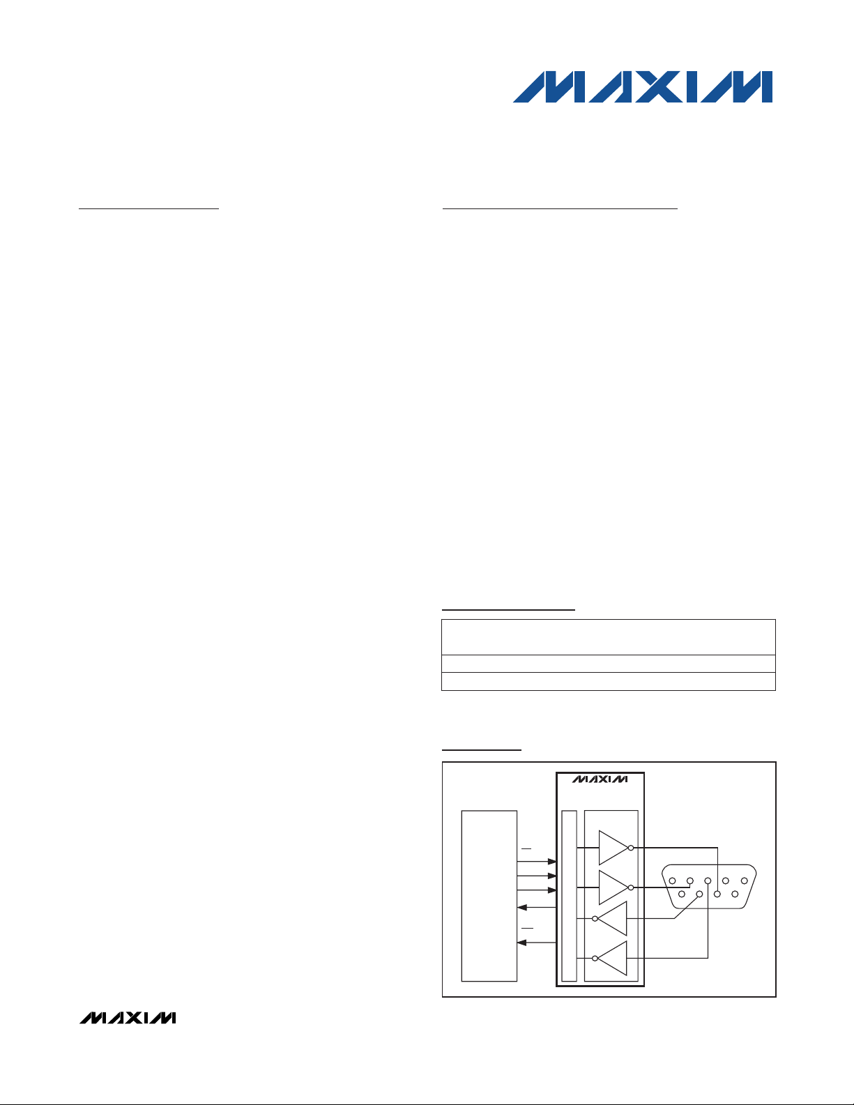
Typical Application Circuit
Ordering Information
SPI and QSPI are trademarks of Motorola, Inc.
MICROWIRE is a trademark of National Semiconductor Corp.
Ordering Information continued at end of data sheet.
Pin Configuration appears at end of data sheet.
†
Covered by U.S. Patent numbers 4,636,930; 4,679,134;
4,777,577; 4,797,899; 4,809,152; 4,897,774; 4,999,761; and
other patents pending.
PART
MAX3110ECWI
MAX3110ECNI 0°C to +70°C
0°C to +70°C
TEMP.
RANGE
PIN-
PACKAGE
28 Wide SO
28 Plastic DIP
V
CC
(V)
5
5
MAX3110E
MAX3111E
SPI
CS
SCLK
DIN
μP
DOUT
IRQ
RS-232
U
A
R
T
12345
678
DB-9
9
Page 2
MAX3110E/MAX3111E
SPI/MICROWIRE-Compatible UART and ±15kV ESDProtected RS-232 Transceivers with Internal Capacitors
2 _______________________________________________________________________________________
ABSOLUTE MAXIMUM RATINGS
ELECTRICAL CHARACTERISTICS—MAX3110E
(VCC= +4.5V to +5.5V, TA = T
MIN
to T
MAX
, unless otherwise noted. Typical values are measured for baud rate set to 9600baud at
V
CC
= +5V, TA= +25°C.) (Note 2)
Stresses beyond those listed under “Absolute Maximum Ratings” may cause permanent damage to the device. These are stress ratings only, and functional operation of the device at these or any other conditions beyond those indicated in the operational sections of the specifications is not implied. Exposure
to absolute maximum rating conditions for extended periods may affect device reliability.
VCCto GND (MAX3110E) ........................................-0.3V to +6V
V
CC
to GND (MAX3111E).........................................-0.3V to +4V
V+ to GND (Note 1) ..................................................-0.3V to +7V
V- to GND (Note 1) ...................................................+0.3V to -7V
V+ to V- (Note 1) ..................................................................+13V
Input Voltages to GND
CS, X1, CTS, RX, DIN, SCLK.................. -0.3V to (V
CC
+ 0.3V)
T_IN, SHDN ...........................................................-0.3V to +6V
R_IN ..................................................................................±25V
Output Voltage to GND
DOUT, RTS, TX, X2 .................................-0.3V to (V
CC
+ 0.3V)
IRQ .......................................................................-0.3V to +6V
T_OUT ...........................................................................±13.2V
R_OUT.....................................................-0.3V to (V
CC
+ 0.3V)
TX, RTS Output Current ....................................................100mA
Short-Circuit Duration
X2, DOUT, IRQ (to V
CC
or GND).............................Continuous
T_OUT (to GND) .....................................................Continuous
Continuous Power Dissipation (T
A
= +70°C)
28-pin Wide SO (derate 12.5mW/°C above +70°C) ...........1W
28-pin Plastic DIP (derate 14.3mW/°C above +70°C) ....1.14W
Operating Temperature Ranges
MAX311_EC_ _ .................................................. 0°C to +70°C
MAX311_EE_ _ ................................................-40°C to +85°C
Storage Temperature Range ............................-65°C to +150°C
Lead Temperature (soldering, 10s) .................................+300°C
Soldering Temperature (reflow)
PDIP lead(Pb)-free ........................................................+225°C
PDIP containing lead(Pb)..............................................+240°C
Wide SO lead(Pb)-free..................................................+225°C
Wide SO containing lead(Pb) .......................................+240°C
Note 1: V+ and V- can have maximum magnitudes of 7V, but their absolute difference should not exceed 13V.
SHDNi bit = 1
SHDNi bit = 0
2
Input Current I
IN1
25
µAVX1= 0 or 5.5V
PARAMETER SYMBOL MIN TYP MAX UNITS
Input Low Voltage V
IL1
0.2V
CC
V
Input High Voltage V
IH1
0.7V
CC
V
V
Supply Current with Hardware
and Software Shutdown
I
CCSHDN(H+ S)
320µA
Input Capacitance C
IN1
5 pF
Input High Voltage V
IH2
0.7V
CC
V
Input Low Voltage V
IL2
0.3V
CC
V
Supply Current I
CC
0.6 2 mA
Supply Current with Hardware
Shutdown
I
CCSHDN(H)
0.48 1 mA
Input Hysteresis V
HYST2
250 mV
Input Leakage Current I
LKG1
±1 µA
Input Capacitance C
IN2
5 pF
Input High Voltage V
IH3
2.4
Input Low Voltage V
IL3
0.8 V
Transmitter Input Hysteresis V
HYST3
500 mV
Input Leakage Current I
IN3
±0.01 ±1 µA
CONDITIONS
SHDN = GND, SHDNi bit = 1 (Note 4)
VCC= 5V
SHDN = VCC, no load
SHDN = GND (Note 3)
DC CHARACTERISTICS (VCC= +5V, TA= +25°C)
UART OSCILLATOR INPUT (X1)
UART LOGIC INPUTS (DIN, SCLK, CS, CTS, RX
))
RS-232 LOGIC INPUTS (T_IN, SHDN
))
Page 3
±25
MAX3110E/MAX3111E
SPI/MICROWIRE-Compatible UART and ±15kV ESD-
Protected RS-232 Transceivers with Internal Capacitors
_______________________________________________________________________________________ 3
ELECTRICAL CHARACTERISTICS—MAX3110E (continued)
(VCC= +4.5V to +5.5V, TA = T
MIN
to T
MAX
, unless otherwise noted. Typical values are measured for baud rate set to 9600baud at
V
CC
= +5V, TA= +25°C.) (Note 2)
CONDITIONS UNITSMIN TYP MAXSYMBOLPARAMETER
mV500V
HYST4
Input Hysteresis
V0.8V
IL4
Input Low Voltage
V2.4V
IH4
Input High Voltage
TA= +25°C kΩ357R
IN
Input Resistance
TA= +25°C, VCC= 5V
TA= +25°C, VCC= 5V
V-25 +25Input Voltage Range
0.9I
SINK
= 25mA; TX only
Output Low Voltage V
OL2
0.4
V
I
SINK
= 4mA; DOUT, RTS
V
CC
- 0.5I
SOURCE
= 10mA; TX only
±8
kV
IEC 1000-4-2 Contact Discharge
±15IEC 1000-4-2 Air Discharge
SCLK Fall to DOUT Valid t
DO
100 nsC
LOAD
= 100pF
CS to SCLK Hold Time
t
CSH
0 ns
Output Low Voltage V
OL1
0.4 V
Output High Voltage V
OH1
VCC- 0.6 V
±0.05 ±10 µA
Output Voltage Swing 5 ±5.4 V
Output Resistance R
O
300 10M Ω
Output Short-Circuit Current ±60 mA
Output Leakage Current I
LKG2
±25 µA
ESD Protection
±15
Output Leakage Current I
LKG3
±1 µA
Output High Voltage V
OH2
V
CC
- 0.5
V
Output Capacitance C
OUT1
5 pF
Output Leakage Current I
LKG4
±1 µA
Output Low Voltage V
OL3
0.4 V
Output Capacitance C
OUT2
5 pF
CS Low to DOUT Valid
t
DV
100 ns
CS High to DOUT Tri-State
t
TR
100 ns
CS to SCLK Setup Time
t
CSS
100 ns
DOUT only, CS = V
CC
I
SINK
= 1.6mA
I
SOURCE
= 1mA
3kΩ load on all transmitter outputs
V
CC
= V+ = V- = 0, V
OUT
= ±2V
I
SOURCE
= 5mA; DOUT, RTS
VCC= 0 or 5.5V, V
OUT
= ±12V,
transmitters disabled
V
IRQ
= 5.5V
I
SINK
= 4mA
Human Body Model
C
LOAD
= 100pF
C
LOAD
= 100pF, RCS= 10kΩ
RS-232 RECEIVER INPUTS (R_IN)
RS-232 ESD PROTECTION (R_IN, T_OUT)
RS-232 RECEIVER OUTPUTS (R_OUT)
RS-232 TRANSMITTER OUTPUTS (T_OUT)
UART OUTPUTS (DOUT, TX, RTS)
UART IRQ OUTPUTS (IRQ = open drain)
UART AC TIMING
Page 4
MAX3110E/MAX3111E
SPI/MICROWIRE-Compatible UART and ±15kV ESDProtected RS-232 Transceivers with Internal Capacitors
4 _______________________________________________________________________________________
ELECTRICAL CHARACTERISTICS—MAX3110E (continued)
(VCC= +4.5V to +5.5V, TA = T
MIN
to T
MAX
, unless otherwise noted. Typical values are measured for baud rate set to 9600baud at
V
CC
= +5V, TA= +25°C.) (Note 2)
CONDITIONS UNITSMIN TYP MAXSYMBOLPARAMETER
ns0t
DH
DIN to SCLK Hold Time
ns100t
DS
DIN to SCLK Setup Time
ns238t
CP
SCLK Period
ns100t
CL
SCLK Low Time
ns100t
CH
SCLK High Time
ns100t
CS0
SCLK Rising Edge to CS Falling
TX, RTS, DOUT; CL= 100pF
ns10t
r
Output Rise Time
ns200t
CSW
CS High Pulse Width
ns200t
CS1
CS Rising Edge to SCLK Rising
Edge
TX, RTS, DOUT, IRQ; CL= 100pF
ns10t
f
Output Fall Time
CL= 150pF to
2500pF
430
V/µs
Receiver Skew |t
PHL
- t
PLH
| 50 ns
CL= 150pF to
1000pF
Transmitter Skew |t
PHL
- t
PLH
| 100 ns
t
PLH
150
ns
Transition-Region Slew Rate
630
Maximum Data Rate 250 kbps
Receiver Propagation Delay
t
PHL
150
(Note 5)
CL= 150pF
VCC= 5V,
RL= 3kΩ to 7kΩ,
T
A
= +25°C,
measured from
+3V to -3V or
-3V to +3V
RL= 3kΩ, CL= 1000pF,
one transmitter switching
Receiver input to receiver output
RS-232 AC TIMING
Page 5
kV
Human Body Model
SPI/MICROWIRE-Compatible UART and ±15kV ESD-
Protected RS-232 Transceivers with Internal Capacitors
_______________________________________________________________________________________ 5
MAX3110E/MAX3111E
SHDN = GND (Note 3)
SHDN = VCC, no load
SHDN = GND SHDNi bit = 1 (Note 4)
CONDITIONS
pF
5
C
IN2
Input Capacitance
µA±1I
LKG1
Input Leakage Current
mV165V
HYST2
Input Hysteresis
mA0.18 0.4I
CCSHDN(H)
Supply Current with Hardware
Shutdown
mA0.45 1.4I
CC
Supply Current
V0.3V
CC
V
IL2
Input Low Voltage
V0.7V
CC
V
IH2
Input High Voltage
pF5C
IN1
µA120I
CCSHDN(H+ S)
Supply Current with Hardware
and Software Shutdown
V
V0.7V
CC
V
IH1
Input High Voltage
V0.2V
CC
V
IL1
Input Low Voltage
UNITSMIN TYP MAXSYMBOLPARAMETER
VX1= 0 or 3.6V µA
25
I
IN1
Input Current
2
SHDNi bit = 0
SHDNi bit = 1
ELECTRICAL CHARACTERISTICS—MAX3111E
(VCC= +3.0V to +3.6V, VA = T
MIN
to T
MAX
, unless otherwise noted. Typical values are measured for baud rate set to 9600baud at
VCC= +3.3V, TA= +25°C.) (Note 2)
TA= +25°C, VCC= 3.3V
VCC= 3.3V
mV500V
HYST4
Input Hysteresis
V0.6V
IL4
Input Low Voltage
V2.4V
IH4
Input High Voltage
µA±0.01 ±1I
IN3
Input Leakage Current
mV500V
HYST3
Transmitter Input Hysteresis
V0.8V
IL3
Input Low Voltage
V2.0V
IH3
Input High Voltage
TA= +25°C kΩ357R
IN
Input Resistance
TA= +25°C, VCC= 3.3V
V-25 +25Input Voltage Range
±15
ESD Protection
IEC 1000-4-2 Air Discharge ±15
IEC 1000-4-2 Contact Discharge ±8
Input Capacitance
DC CHARACTERISTICS (VCC= 3.3V, TA= +25°C)
UART OSCILLATOR INPUT (X1)
UART LOGIC INPUTS (DIN, SCLK, CS, RX
))
RS-232 LOGIC INPUTS (T_IN, SHDN)
RS-232 RECEIVER INPUTS (R_IN)
RS-232 ESD PROTECTION (R_IN, T_OUT)
Page 6
MAX3110E/MAX3111E
SPI/MICROWIRE-Compatible UART and ±15kV ESDProtected RS-232 Transceivers with Internal Capacitors
6 _______________________________________________________________________________________
ELECTRICAL CHARACTERISTICS—MAX3111E (continued)
(VCC= +3.0V to +3.6V, VA = T
MIN
to T
MAX
, unless otherwise noted. Typical values are measured for baud rate set to 9600baud at
V
CC
= +3.3V, TA= +25°C.) (Note 2)
Output Fall Time t
f
10 ns
TX, RTS, DOUT, IRQ; C
LOAD
= 100pF
CS Rising Edge to SCLK Rising
Edge
t
CS1
200 ns
CS High Pulse Width
t
CSW
200 ns
Output Rise Time t
r
10 ns
TX, RTS, DOUT; C
LOAD
= 100pF
SCLK Rising Edge to CS Falling
t
CS0
100 ns
SCLK High Time t
CH
100 ns
SCLK Low Time t
CL
100 ns
SCLK Period t
CP
238 ns
SCLK Fall to DOUT Valid t
DO
100 ns
DIN to SCLK Setup Time t
DS
100 ns
DIN to SCLK Hold Time t
DH
0 ns
C
LOAD
= 100pF
CS to SCLK Hold Time
t
CSH
0 ns
CS Low to DOUT Valid
t
DV
100 ns
CS High to DOUT Tri-State
t
TR
100 ns
CS to SCLK Setup Time
t
CSS
100 ns
C
LOAD
= 100pF
C
LOAD
= 100pF, RCS= 10kΩ
0.9I
SINK
= 25mA, TX only
Output Low Voltage V
OL2
0.4
V
±25
V
CC
- 0.5
I
SINK
= 4mA; DOUT, RTS
Output Low Voltage V
OL1
0.4 V
Output High Voltage V
OH1
VCC- 0.6 V
Output Voltage Swing ±5 ±5.4 V
Output Resistance R
O
300 10M Ω
Output Short-Circuit Current ±60 mA
Output Leakage Current I
LKG2
µA
I
SOURCE
= 10mA, TX only
PARAMETER SYMBOL MIN TYP MAX UNITS
Output Leakage Current I
LKG3
±1 µA
Output High Voltage V
OH2
V
CC
- 0.5
V
Output Capacitance C
OUT1
5 pF
Output Leakage Current I
LKG4
±1 µA
Output Low Voltage V
OL3
0.4 V
Output Capacitance C
OUT2
5 pF
DOUT only; CS = V
CC
I
SINK
= 1.6mA
I
SOURCE
= 1mA
3kΩ load on all transmitter outputs
V
CC
= V+ = V- = 0, V
OUT
= ±2V
I
SOURCE
= 5mA; DOUT, RTS
VCC= 0 or 3.6V, V
OUT
= ±12V,
transmitters disabled
V
IRQ
= 3.6V
I
SINK
= 4mA
CONDITION
RS-232 RECEIVER OUTPUTS (R_OUT)
RS-232 TRANSMITTER OUTPUTS (T_OUT)
UART OUTPUTS (DOUT, TX, RTS)
UART IRQ OUTPUT (IRQ = open drain)
UART AC TIMING
Page 7
ns
MAX3110E/MAX3111E
SPI/MICROWIRE-Compatible UART and ±15kV ESD-
Protected RS-232 Transceivers with Internal Capacitors
_______________________________________________________________________________________ 7
ELECTRICAL CHARACTERISTICS—MAX3111E (continued)
(VCC= +3.0V to +3.6V, VA = T
MIN
to T
MAX
, unless otherwise noted. Typical values are measured for baud rate set to 9600baud at
V
CC
= +3.3V, TA= +25°C.) (Note 2)
Note 2: All currents into the device are positive; all currents out of the device are negative. All voltages are referred to device
ground unless otherwise noted.
Note 3: I
CCSHDN(H)
represents a hardware-only shutdown. In hardware shutdown, the UART is in normal operation and the charge
pumps for the RS-232 transmitters are shut down.
Note 4: I
CCSHDN(H+S)
represents a simultaneous software and hardware shutdown in which the UART and charge pumps are
shut down.
Note 5: Transmitter skew is measured at the transmitter zero cross points.
Receiver input to receiver output
RL= 3kΩ, CL= 1000pF,
one-transmitter switching
VCC= 3.3V,
RL= 3kΩ to 7kΩ,
TA= +25°C,
measured from
+3V to -3V or
-3V to +3V
CL= 150pF
(Note 5)
150t
PHL
Receiver Propagation Delay
kbps250Maximum Data Rate
V/µs
630
Transition-Region Slew Rate
ns
150t
PLH
CL= 150pF to
1000pF
ns200|t
PHL
- t
PLH
| Transmitter Skew
ns100|t
PHL
- t
PLH
| Receiver Skew
430
CL= 150pF to
2500pF
CONDITIONS UNITSMIN TYP MAXSYMBOLPARAMETER
RS-232 AC TIMING
Page 8
MAX3110E/MAX3111E
SPI/MICROWIRE-Compatible UART and ±15kV ESDProtected RS-232 Transceivers with Internal Capacitors
8 _______________________________________________________________________________________
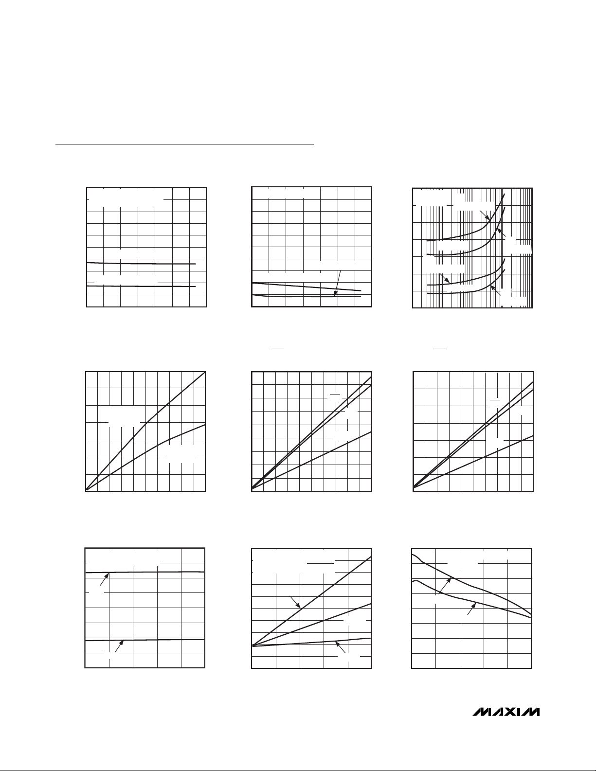
Typical Operating Characteristics
(TA = +25°C, unless otherwise noted.)
UART SUPPLY CURRENT vs. TEMPERATURE
1000
1.8432MHz CRYSTAL
900
TRANSMITTING AT 115.2kbps
800
700
600
500
400
300
SUPPLY CURRENT (μA)
200
100
0
MAX3110E, VCC = +5V
MAX3111E, VCC = +3.3V
-40 -20 40 60 100
020 80
TEMPERATURE (°C)
10
MAX3110E-01
SHUTDOWN CURRENT (μA)
UART SHUTDOWN CURRENT
vs. TEMPERATURE
1.8432MHz CRYSTAL
9
8
7
6
5
4
3
2
1
0
MAX3110E, VCC = +5V
-40 -20 40 60 100
MAX3111E, VCC = +3.3V
020 80
TEMPERATURE (°C)
MAX3110E-02
400
1.8432MHz
CRYSTAL
350
300
250
200
SUPPLY CURRENT (μA)
150
100
+3V
TRANSMITTING
50
100 10k
UART SUPPLY CURRENT
vs. BAUD RATE
+5V
TRANSMITTING
MAX3110E
MAX3111E
1000
BAUD RATE (bps)
+3V
STANDBY
100k 1M
+5V
STANDBY
MAX3110E-03
UART SUPPLY CURRENT vs.
700
600
500
400
300
SUPPLY CURRENT (μA)
200
100
EXTERNAL CLOCK FREQUENCY
MAX3110E
= +5V
V
CC
0
01 3
EXTERNAL CLOCK FREQUENCY (MHz)
2
MAX3111E
V
= +3.3V
CC
4
MAX3110E-04
5
RS-232 TRANSMITTER OUTPUT VOLTAGE
vs. OUTPUT LOW VOLTAGE (V
90
80
70
60
50
40
30
OUTPUT SINK CURRENT (mA)
20
10
0
0 0.20.1 0.6 0.7
RS-232 TRANSCEIVER SUPPLY CURRENT
vs. LOAD CAPACITANCE
10.0
TRANSMITTER 1 AT 250kbps
TRANSMITTER 2 AT 15.6kbps
7.5
3kΩ + C
L
5.0
V
OUT+
2.5
0
-2.5
-5.0
TRANSMITTER OUTPUT VOLTAGE (V)
-7.5
-10.0
V
OUT-
0 1000 2000 3000 4000 5000
LOAD CAPACITANCE (pF)
MAX3110E/TOC07
50
45
40
35
30
25
20
15
SUPPLY CURRENT (mA)
10
5
0
0 1000 2000
TX, RTS, DOUT OUTPUT CURRENT
MAX3110E
= +5V)
CC
RTS
TX
DOUT
0.3 0.50.4 0.9
VOLTAGE (V)
0.8
vs. LOAD CAPACITANCE
TRANSMITTER 1 AT DATA RATE
TRANSMITTER 2 AT DATA RATE
3kΩ + C
L
250kbps
LOAD CAPACITANCE (pF)
16
120kbps
20kbps
3000 4000 5000
vs. OUTPUT LOW VOLTAGE (V
70
MAX3110E-06
60
50
40
30
20
OUTPUT SINK CURRENT (mA)
10
MAX3110E/TOC09
SLEW RATE (V/μs)
0
16
14
12
10
8
6
4
2
0
0 1000 2000 3000 4000 5000
1.0
TX, RTS, DOUT OUTPUT CURRENT
MAX3111E
CC
RTS
DOUT
0 0.20.1 0.6 0.7
0.3 0.50.4 0.9
VOLTAGE (V)
RS-232 TRANSMITTER SLEW RATE
vs. LOAD CAPACITANCE
TRANSMITTER 1 AT 250kbps
3kΩ + C
L
-SLEW
+SLEW
LOAD CAPACITANCE (pF)
= +3.3V)
TX
0.8
MAX3110E-05
1.0
MAX3110E/TOC11
Page 9

MAX3110E/MAX3111E
SPI/MICROWIRE-Compatible UART and ±15kV ESD-
Protected RS-232 Transceivers with Internal Capacitors
_______________________________________________________________________________________ 9
Pin Description
Positive terminal of internal inverting charge-pump capacitor. Do not make any connection to this terminal.
C2+24
Negative terminal of internal inverting charge-pump capacitor. Do not make any connection to this terminal.
C2-25
-5.5V generated by the internal charge pump. Do not make any connection to this terminal.
V-26
GroundGND27
RS-232 Transmitter Output 2T2OUT28
UART Active-Low Interrupt Output. Open-drain interrupt output to microprocessor.
IRQ
19
Hardware Shutdown Input. Drive SHDN low to shut down the RS-232 transmitters and charge pump. Drive
high for normal operation.
SHDN
20
+5.5V generated by the internal charge pump. Do not make any connection to this terminal.
V+21
Positive terminal of the internal voltage-doubler charge-pump capacitor. Do not make any connection to
this terminal.
C1+22
Negative terminal of the internal voltage-doubler charge-pump capacitor. Do not make any connection to
this terminal.
C1-23
SPI/MICROWIRE Serial-Data Input. Schmitt-trigger Input.DIN15
SPI/MICROWIRE Serial-Data Output. High impedance when CS is high.
DOUT16
SPI/MICROWIRE Serial-Clock Input. Schmitt-trigger input.SCLK17
UART Active-Low Chip-Select Input. DOUT goes high impedance when CS is high. IRQ, TX, and RTS are
always active. Schmitt-trigger input.
CS
18
UART Asynchronous Serial-Data (transmitter) OutputTX14
UART Crystal Connection. Leave X2 unconnected when using an external CMOS clock. See the
Crystals,
Oscillators, and Ceramic Resonators
section.
X29
UART Crystal Connection. X1 also serves as an external CMOS clock input. See the
Crystals, Oscillators,
and Ceramic Resonators
section.
X110
UART Clear-to-Send Active-Low Input. Read via the CTS bit.
CTS
11
UART Request-to-Send Active-Low Output. Controlled by the RTS bit. Also used to control the driver enable
in RS-485 networks.
RTS
12
UART Asynchronous Serial-Data (receiver) Input. The serial information received from the RS-232 receiver.
A transition on RX while in shutdown generates an interrupt (Table 1).
RX13
RS-232 Receiver Output 1, TTL/CMOSR1OUT5
RS-232 Receiver Input 1R1IN6
RS-232 Transmitter Output 1T1OUT7
Positive Supply VoltageV
CC
8
RS-232 Transmitter lnput 1, TTL/CMOST1IN4
RS-232 Transmitter lnput 2, TTL/CMOST2IN3
PIN
RS-232 Receiver Output 2, TTL/CMOSR2OUT2
RS-232 Receiver Input 2R2IN1
FUNCTIONNAME
Page 10
MAX3110E/MAX3111E
SPI/MICROWIRE-Compatible UART and ±15kV ESDProtected RS-232 Transceivers with Internal Capacitors
10 ______________________________________________________________________________________
Detailed Description
The MAX3110E/MAX3111E contain an SPI/QSPI/MICROWIREcompatible UART and an RS-232 transceiver with two
drivers and two receivers. The UART is compatible with
SPI and QSPI for CPOL = 0 and CPHA = 0. The UART
supports data rates up to 230kbaud for standard UART
bit streams as well as IrDA and includes an 8-word
receive FIFO. Also included is a 9-bit-address recognition interrupt.
The RS-232 transceiver has electrostatic discharge
(ESD) protection on the transmitter outputs and the
receiver inputs. The internal charge-pump capacitors
minimize the number of external components required.
The RS-232 transceivers meet EIA/TIA-232 specifica-
tions for V
CC
down to the minimum supply voltage and
are guaranteed to operate for data rates up to 250kbps.
The UART and RS-232 functions operate as one device
or independently since the two functions share only
supply and ground connections.
UART
The universal asynchronous receiver transmitter
(UART) interfaces the SPI/QSPI/MICROWIRE-compatible synchronous serial data from a microprocessor (µP)
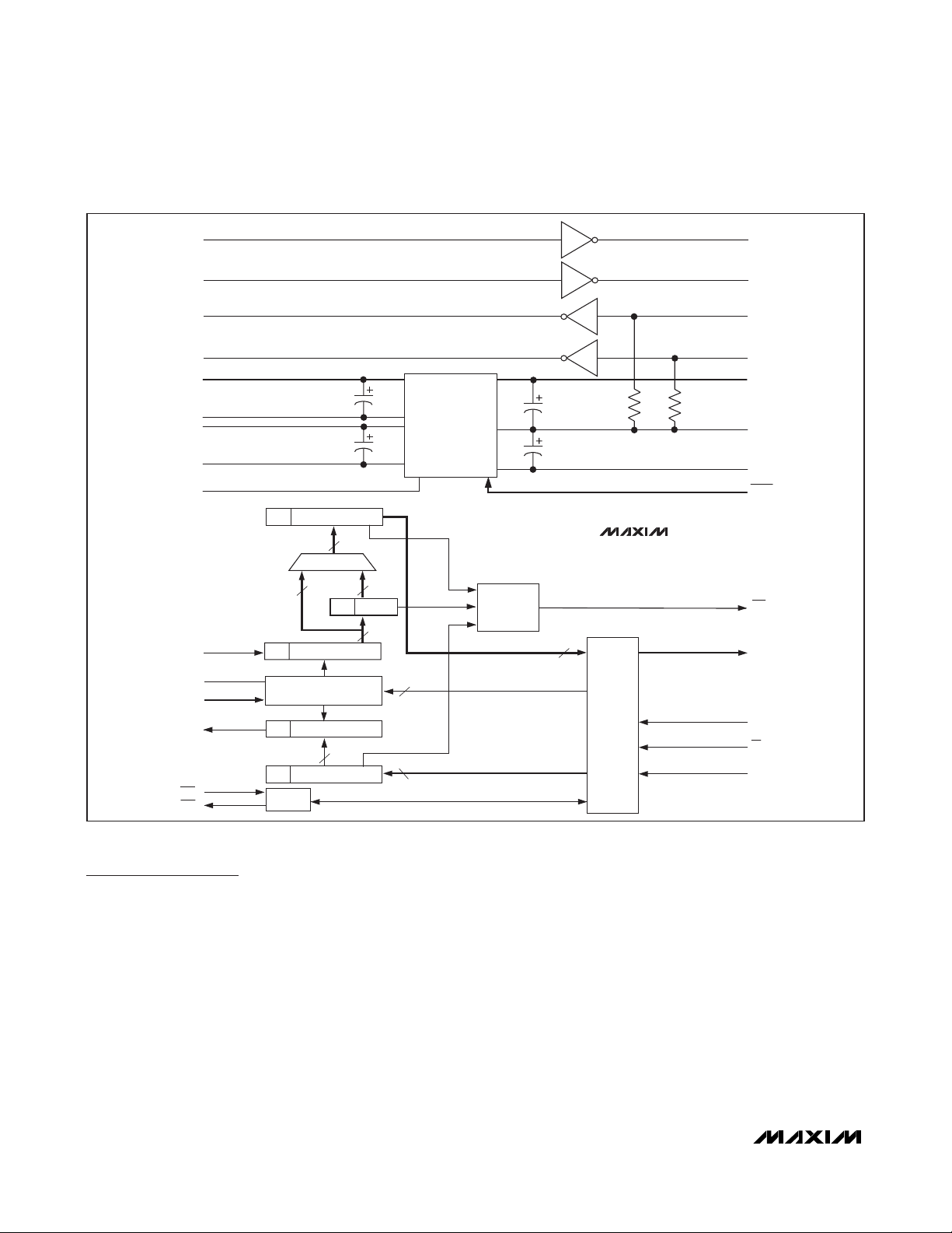
to asynchronous, serial-data communication ports (RS232, IrDA). Figure 1 shows the MAX3110E/MAX3111E
functional diagram. Included in the UART function is an
SPI/QSPI/MICROWIRE interface, a baud-rate generator,
and an interrupt generator.
Figure 1. MAX3110E/MAX3111E Functional Diagram
T2IN
T1IN
R2OUT
R1OUT
C1+
INTERNAL
C1-
C2+
INTERNAL
C2-
V
CC
Pr RX BUFFER
9
RX
X2
X1
TX
CTS
RTS
9
RX SHIFT REGISTER
Pr
GENERATOR
TX SHIFT REGISTER
Pt
Pt TX BUFFER
I/O
9
Pr RX FIFO
9
BAUD-RATE
4
9
9
CHARGE
PUMP
INTERRUPT
LOGIC
INTERNAL
INTERNAL
MAX3110E/MAX3111E
9
5k
SPI
INTERFACE
T2OUT
T1OUT
R2IN
R1IN
V+
5k
GND
V-
SHDN
IRQ
DOUT
SCLK
CS
DIN
Page 11

MAX3110E/MAX3111EMAX3110E/MAX3111E
SPI/MICROWIRE-Compatible UART and ±15kV ESD-
Protected RS-232 Transceivers with Internal Capacitors
______________________________________________________________________________________ 11
SPI Interface
The MAX3110E/MAX3111E are compatible with SPI,
QSPI (CPOL = 0, CPHA = 0), and MICROWIRE serialinterface standards (Figure 2). The MAX3110E/
MAX3111E have a unique full-duplex-only architecture
that expects a 16-bit word for DIN and simultaneously
produces a 16-bit word for DOUT regardless of which
read/write register is used. The DIN stream is monitored for its first two bits to tell the UART the type of
data transfer being executed (see the
Write
Configuration Register, Read Configuration Register
,
Write Data Register
, and
Read Data Registe
r sections).
DIN (MOSI) is latched on SCLK’s rising edge. DOUT
(MISO) should be read into the µP on SCLK’s rising
edge. The first bit (bit 15) of DOUT transitions on CS’s
falling edge, and bits 14–0 transition on SCLK’s falling
edge. Figure 3 shows the detailed serial timing specifications for the synchronous SPI port.
Only 16-bit words are expected. If CS goes high in the
middle of a transmission (any time before the 16th bit),
the sequence is aborted (i.e., data does not get written
to individual registers). Most operations, such as the
clearing of internal registers, are executed only on CS’s
rising edge. Every time CS goes low, a new 16-bit
stream is expected. An example of using the Write
Configuration Register is shown in Figure 4.
Table 1 describes the bits located in the Write Configuration, Read Configuration, Write Data, and Read
Data Registers. This table also describes whether the
bit is a read or a write bit and the power-on reset state
(POR) of the bits. Figure 5 shows an example of parity
and word-length control.
Figure 2. Compatible CPOL and CPHA Timing Modes
Figure 3. Detailed Serial Timing Specifications for the Synchronous SPI Port
MSB 1314 12 11 10 9 8 7 6 5 4 3 2 1 LSB
DIN
DOUT
SCLK
SCLK
MSB 1314 12 11 10 9 8 7 6 5 4 3 2 1 LSB
CS
(CPOL = 0, CPHA = 0)
(CPOL = 0, CPHA = 1)
COMPATIBLE
WITH MAX3110E/MAX3111E
SCLK
(CPOL = 1, CPHA = 0)
SCLK
(CPOL = 1, CPHA = 1)
SCLK
DIN
DOUT
CS
t
t
CSO
CSS
t
DS
t
DH
t
DV
t
CL
• • •
t
CH
• • •
• • •
• • •
NOT COMPATIBLE
WITH MAX3110E/MAX3111E
t
CSH
t
DO
t
CS1
t
TR
Page 12

MAX3110E/MAX3111E
12 ______________________________________________________________________________________
SPI/MICROWIRE-Compatible UART and ±15kV ESDProtected RS-232 Transceivers with Internal Capacitors
Figure 4. Write Configuration Register Example
Figure 5. Parity and Word-Length Control
DATA
UPDATED
CS
SCLK
DIN
DOUT
15
14 13 12 11 10 9 8 7 6 5 4 3 2 1 0
11 FEN SHDN TM RM PM RAM IR ST PE L B3 B2 B1 B0
RT 00 000 00 00000 00
PE = 0, L = 0
IDLE
IDLE
IDLE
IDLE
TIME
D0START D1 D2 D3 D4 D5 D6 D7 STOP STOP IDLE
PE = 0, L = 1
D0START D1 D2 D3 D4 D5 D6 STOP STOP IDLE
PE = 1, L = 0
D0START D1 D2 D3 D4 D5 D6 D7 Pt STOP STOP IDLE
PE = 1, L = 1
D0START D1 D2 D3 D4 D5 D6 Pt
STOPSTOP
IDLE
SECOND STOP BIT IS OMITTED IF ST = 0.
Page 13

MAX3110E/MAX3111E
SPI/MICROWIRE-Compatible UART and ±15kV ESD-
Protected RS-232 Transceivers with Internal Capacitors
______________________________________________________________________________________ 13
Table 1. Bit Descriptions
0PE
POR
STATE
write
Parity-Enable Bit. Appends the Pt bit to the transmitted data when PE = 1, and sends the Pt bit
as written. No parity bit is transmitted when PE = 0. With PE = 1, an extra bit is expected to be
received. This data is put into the Pr register. Pr = 0 when PE = 0. The MAX3110E/MAX3111E
do not calculate parity.
0PE read Reads the value of the Parity-Enable bit.
0
PM
write
Mask for Pr bit. IRQ is asserted if PM = 1 and Pr = 1 (Table 7).
DESCRIPTION
0000
0000
XPr read
Receive-Parity Bit. This bit is the extra bit received if PE = 1. Therefore, PE = 1 results in 9-bit
transmissions (L = 0). If PE = 0, then Pr is set to 0. Pr is stored in the FIFO with the receive data
(see the
9-Bit Networks
section).
0
0
IR read Reads the value of the IR bit.
L
BIT
TYPE
write
B0–B3 write Baud-Rate Divisor Select Bits. Sets the baud clock’s value (Table 6).
B0–B3 read Baud-Rate Divisor Select Bits. Reads the 4-bit baud clock value assigned to these registers.
BIT
NAME
Bit to set the word length of the transmitted or received data. L = 0 results in 8-bit words
(9-bit words if PE = 1) (see Figure 5). L = 1 results in 7-bit words (8-bit words if PE = 1).
0
X
L read Reads the value of the L bit.
Pt write
Transmit-Parity Bit. This bit is treated as an extra bit that is transmitted if PE = 1. In 9-bit networks, the MAX3110E/MAX3111E do not calculate parity. If PE = 0, then this bit (Pt) is ignored
in transmit mode (see the
9-Bit Networks
section).
00000000
0
D0r–D7r read
Eight data bits read from the receive FIFO or the receive-buffer register. When L = 1, D7r is
always 0.
FEN
write
FIFO Enable. Enables the receive FIFO when FEN = 0. When FEN = 1, FIFO is disabled.
0
0
FEN
read
FIFO-Enable Readback. FEN’s state is read.
IR write Enables the IrDA timing mode when IR = 1.
No
change
XXXXXXXX
CTS read
Clear-to-Send-Input. Records the state of the CTS pin (CTS bit = 0 implies CTS pin = logic
high).
D0t–D7t write
Transmit-Buffer Register. Eight data bits written into the transmit-buffer register. D7t is ignored
when L = 1.
0
PM
read
Reads the value of the PM bit (Table 7).
0R read
Receive Bit or FIFO Not Empty Flag. R = 1 means new data is available to be read or is being
read from the receive register or FIFO. If performing a Read Data or Write Data operation, the R
bit will clear on the falling edge of SCLK's 16th pulse if no new data is available.
0
RM
write
Mask for R bit. IRQ is asserted if RM = 1 and R = 1 (Table 7).
0
RM
read
Reads the value of the RM bit (Table 7).
0
RAM
write
Mask for RA/FE bit. IRQ is asserted if RAM = 1 and RA/FE = 1 (Table 7).
0
RAM
read
Reads the value of the RAM bit (Table 7).
0RTS write
Request-to-Send Bit. Controls the state of the RTS output. This bit is reset on power-up (RTS
bit = 0 sets the RTS pin = logic high).
Page 14

MAX3110E/MAX3111E
SPI/MICROWIRE-Compatible UART and ±15kV ESDProtected RS-232 Transceivers with Internal Capacitors
14 ______________________________________________________________________________________
Notice to High-Level Programmers: The UART follows
the SPI convention of providing a bidirectional data path
for writes and reads. Whenever the data is written, data
is also read back. This speeds operation over the SPI
bus, and the UART needs this speed advantage when
operating at high baud rates. In most high-level languages, such as C, there are commands for writing and
reading stream I/O devices such as the console or serial
port. In C specifically, there is a “PUTCHAR” command
that transmits a character and a “GETCHAR” command
that receives a character. If programmers were to write
direct write and read commands in C with no underlying
driver code, they would notice that a PUTCHAR command is really a PUTGETCHAR command. These C
commands assume some form of BIOS-level support for
these commands. The proper way to implement these
commands is to write driver code, usually in the form of
an assembly-language interrupt-service routine and a
callable routine used by high-level routines. This driver
handles the interrupts and manages the receive and
transmit buffers for the MAX3110E/MAX3111E. When a
PUTCHAR executes, this driver is called and it safely
buffers any characters received when the current
character is transmitted. When a GETCHAR executes, it
checks its own receive buffer before getting data from
the UART. See the C-language
Outline for a MAX3110E/
MAX3111E Software Driver
in Listing 1, which appears at
the end of this data sheet.
Listing 1 is a C-language outline of an interrupt-driven
software driver that interfaces to a MAX3110E/
MAX3111E, providing an intermediate layer between
the bit-manipulation subroutine and the familiar
PUTCHAR/GETCHAR subroutines.
The user must supply code for managing the transmit
and receive queues as well as the low-level hardware
interface itself. The interrupt control hardware must be
initialized before this driver is called.
Table 1. Bit Descriptions (continued)
POR
STATE
DESCRIPTION
BIT
TYPE
BIT
NAME
0SHDNi write
Software-Shutdown Bit. Enter software shutdown with a Write Configuration where SHDNi = 1.
Software shutdown takes effect after CS goes high, and causes the oscillator to stop as soon
as the transmitter becomes idle. Software shutdown also clears R, T, RA/FE, D0r–D7r,
D0t–D7t, Pr, Pt, and all data in the receive FIFO. RTS and CTS can be read and updated
while in shutdown. Exit software shutdown with a Write Configuration where SHDNi = 0. The
oscillator restarts typically within 50ms of CS going high. RTS and CTS are unaffected. Refer
to the
Pin Description
for hardware shutdown (SHDN input).
0SHDNo read
Shutdown Read-Back Bit. The Read Configuration register outputs SHDNo = 1 when the
UART is in shutdown. Note that this bit is not sent until the current byte in the transmitter is
sent (T = 1). This tells the processor when it may shut down the RS-485/RS-422 driver. This bit
is also set immediately when the device is shut down through the SHDN pin.
0RA/FE read
Receiver-Activity/Framing-Error Bit. In shutdown mode, this is the RA bit. In normal operation,
this is the FE bit. In shutdown mode, a transition on RX sets RA = 1. In normal mode, a framing error sets FE = 1. A framing error occurs if a zero is received when the first stop bit is
expected. FE is set when a framing error occurs, and cleared upon receipt of the next properly framed character independent of the FIFO being enabled. When the device wakes up, it is
likely that a framing error will occur. This error is cleared with a Write Configuration. The FE bit
is not cleared on a Read Data operation. When an FE is encountered, the UART resets itself
to the state where it is looking for a start bit.
0ST write
Transmit-Stop Bit. One stop bit will be transmitted when ST = 0. Two stop bits will be transmitted when ST = 1. The receiver only requires one stop bit.
0ST read Reads the value of the ST bit.
0
TM
write
Mask for T Bit. IRQ is asserted if TM = 1 and T = 1 (Table 7).
0
TM
read
Reads the value of the TM bit (Table 7).
1T read
Transmit-Buffer-Empty Flag. T = 1 means that the transmit buffer is empty and ready to
accept another data word.
0
TE
write
Transmit-Enable Bit. If TE = 1, then only the RTS pin is updated on CS’s rising edge. The contents of RTS, Pt, and D0t–D7t transmit on CS’s rising edge when TE = 0.
Page 15

MAX3110E/MAX3111E
Write Configuration Register (D15, D14 = 1, 1)
Configure the UART by writing a 16-bit word to the write
configuration register, which programs the baud rate,
data word length, parity enable, and enable of the 8word receive FIFO. In this mode, bits 15 and 14 of the
DIN configuration word are both required to be 1 in
order to enable the write configuration mode. Bits 13–0
of the DIN configuration word set the configuration of
the UART. Table 2 shows the bit assignment for the
write configuration register. The write configuration register allows selection between normal UART timing and
IrDA timing, provides shutdown control, and contains
four interrupt mask bits.
Using the write configuration register clears the receive
FIFO and the R, T, RA/FE, D0r–D7r, D0t–D7t, Pr, and Pt
registers. RTS and CTS remain unchanged. The new
configuration is valid on CS’s rising edge if the transmit
buffer is empty (T = 1) and transmission is over. If the
latest transmission has not been completed (T = 0), the
registers are updated when the transmission is over.
The write configuration register bits (FEN, SHDNi, IR,
ST, PE, L, B3–B0) take effect after the current transmission is over. The mask bits (TM, RM, PM, RAM) take
effect immediately after SCLK’s 16th rising edge.
Bits 15 and 14 of the DOUT write configuration (R and
T) are sent out of the MAX3110E/MAX3111E along with
14 trailing zeros. The use of the R and T bits is optional,
but ignore the 14 trailing zeros.
Warning! The UART requires stable crystal oscillator
operation before configuration (typically ~25ms after
power-up). Upon power-up, compare the write configuration bits with the read configuration bits in a software
loop until both match. This ensures that the oscillator is
stable and that the UART is configured correctly.
Read Configuration Register (D15, D14 = 0, 1)
The read configuration register is used to read back the
last configuration written to the UART. In this register,
bits 15 and 14 of the DIN configuration word are
required to be 0 and 1, respectively, to enable the read
configuration mode. Bits 13–1 of the DIN word should
be zeros, and bit 0 is the test bit to put the UART in test
mode (see the
Test Mode
section). Table 3 shows the
bit assignment for the read configuration register.
Test Mode
The device enters a test mode if bit 0 of the DIN configuration word equals one when doing a read configuration. In this mode, if CS = 0, the RTS pin transmits a
clock that is 16-times the baud rate. The TX pin is low
as long as CS remains low while in test mode. Table 3
shows the bit assignment for the read configuration
register.
Write Data Register (D15, D14 = 1, 0)
Use the write data register for transmitting to the TXbuffer and receiving from the RX buffer (and RX FIFO
when enabled). When using this register, the DIN and
DOUT write data words are used simultaneously, and
bits 13–11 for both the DIN and DOUT write data words
are meaningless zeros. The DIN write data word contains the data that is being transmitted, and the DOUT
write data word contains the data that is being received
from the RX FIFO. Table 4 shows the bit assignment for
the write data mode. To change the RTS pin’s output
state without transmitting data, set the TE bit high. If
performing a write data operation, the R bit will clear on
the falling edge of SCLK’s 16th clock pulse if no new
data is available.
Read Data Register (D15, D14 = 0, 0)
Use the read data register for receiving data from the
RX FIFO. When using this register, bits 15 and 14 of
DIN are both required to be 0. Bits 13–0 of the DIN
read-data word should be zeros. Table 5 shows the bit
assignments for the read data mode. Reading data
clears the R bit and interrupt IRQ. If performing a read
data operation, the R bit will clear on the falling edge of
SCLKs 16th clock pulse if no new data is available.
SPI/MICROWIRE-Compatible UART and ±15kV ESD-
Protected RS-232 Transceivers with Internal Capacitors
______________________________________________________________________________________ 15
Page 16

MAX3110E/MAX3111E
SPI/MICROWIRE-Compatible UART and ±15kV ESDProtected RS-232 Transceivers with Internal Capacitors
16 ______________________________________________________________________________________
6
ST
0
7
IR
0
2
B2
0
3
B3
0
0
B0
0
1
B1
0
4
L
0
5
PE
0
10
RM
0
11
TM
0
8
RAM
0
9
PM
0
12
SHDNi
0
13
FEN
0
15 14
1
T
DIN 1
DOUT R
BIT
Table 2. Write Configuration (D15, D14 = 1, 1)
Notes:
bit 15: DOUT
R = 1, Data is available to be read or is being read from the
receive register or FIFO.
R = 0, Receive register and FIFO are empty.
bit 14: DOUT
T = 1, Transmit buffer is empty.
T = 0, Transmit buffer is full.
bits 13–0: DOUT
Zeros
bits 15, 14: DIN
1,1 = Write Configuration
bit 13: DIN
FEN = 0, FIFO is enabled.
FEN = 1, FIFO is disabled.
bit 12: DIN
SHDNi = 1, Enter software shutdown.
SHDNi = 0, Exit software shutdown.
bit 11: DIN
TM = 1, Transmit buffer empty interrupt is enabled.
TM = 0, Transmit buffer empty interrupt is disabled.
bit 10: DIN
RM = 1, Data available in the receive register or FIFO interrupt
is enabled.
RM = 0, Data available in the receive register or FIFO interrupt
is disabled.
bit 9: DIN
PM = 1, Parity bit high received interrupt is enabled.
PM = 0, Parity bit received interrupt is disabled.
bit 8: DIN
RAM = 1, Receiver-activity (shutdown mode)/Framing-error
(normal operation) interrupt is enabled.
RAM = 0, Receiver-activity (shutdown mode)/Framing-error
(normal operation) interrupt is disabled.
bit 7: DIN
IR = 1, IrDA mode is enabled.
IR = 0, IrDA mode is disabled.
bit 6: DIN
ST = 1, Transmit two stop-bits.
ST = 0, Transmit one stop-bit.
bit 5: DIN
PE = 1, Parity is enabled for both transmit (state of Pt) and
receive.
PE = 0, Parity is disabled for both transmit and receive.
bit 4: DIN
L = 1, 7-bit words (8-bit words if PE = 1)
L = 0, 8-bit words (9-bit words if PE = 1)
bits 3–0: DIN
B3–B0 = XXXX, Baud-Rate Divisor Select Bits (see Table 6)
D15 is present at DOUT on CS’s falling edge. Consecutive bits are clocked out on SCLK’s falling edge.
Page 17

MAX3110E/MAX3111E
SPI/MICROWIRE-Compatible UART and ±15kV ESD-
Protected RS-232 Transceivers with Internal Capacitors
______________________________________________________________________________________ 17
Table 3. Read Configuration (D15, D14 = 0, 1)
Notes:
bit 15: DOUT
R = 1, Data is available to be read or is being read from the
receive register or FIFO.
R = 0, Receive register and FIFO are empty.
bit 14: DOUT
T = 1, Transmit buffer is empty.
T = 0, Transmit buffer is full.
bit 13: DOUT
FEN = 0, FIFO is enabled.
FEN = 1, FIFO is disabled.
bit 12: DOUT
SHDNo = 1, Software shutdown is enabled.
SHDNo = 0, Software shutdown is disabled.
bit 11: DOUT
TM = 1, Transmit buffer empty interrupt is enabled.
TM = 0, Transmit buffer empty interrupt is disabled.
bit 10: DOUT
RM = 1, Data available in the receive register or FIFO interrupt
is enabled.
RM = 0, Data available in the receive register or FIFO interrupt
is disabled.
bit 9: DOUT
PM = 1, Parity bit high received interrupt is enabled.
PM = 0, Parity bit received interrupt is disabled.
bit 8: DOUT
RAM = 1, Receiver-activity (shutdown mode)/Framing-error
(normal operation) interrupt is enabled.
RAM = 0, Receiver-activity (shutdown mode)/Framing-error
(normal operation) interrupt is disabled.
bit 7: DOUT
IR = 1, IrDA mode is enabled.
IR = 0, IrDA mode is disabled.
bit 6: DOUT
ST = 1, Transmit two stop-bits.
ST = 0, Transmit one stop-bit.
bit 5: DOUT
PE = 1, Parity is enabled for both transmit (state of Pt) and
receive.
PE = 0, Parity is disabled for both transmit and receive.
bit 4: DOUT
L = 1, 7-bit words (8-bit words if PE = 1)
L = 0, 8-bit words (9-bit words if PE = 1)
bits 3–0: DOUT
B3–B0 = XXXX Baud-Rate Divisor Select Bits (see Table 6)
bit 15, 14: DIN
0,1 = Read Configuration
bits 13–1: DIN
Zeros
bit 0: DIN
If TEST = 1 and CS = 0, then RTS =16xBaudCLK
TEST = 0, Disables test mode
D15 is present at DOUT on CS’s falling edge. Consecutive bits are clocked out on SCLK’s falling edge.
14
1
T
6
0
ST
7
0
IR
15 2
DIN 0 0
DOUT R B2
BIT 3
0
B3
0
TEST
B0
1
0
B1
4
0
L
5
0
PE
10
0
RM
11
0
TM
8
0
RAM
9
0
PM
12
0
SHDNo
13
0
FEN
Page 18

MAX3110E/MAX3111E
SPI/MICROWIRE-Compatible UART and ±15kV ESDProtected RS-232 Transceivers with Internal Capacitors
18 ______________________________________________________________________________________
Table 4. Write Data (D15, D14 = 1, 0)
Notes:
bit 15: DOUT
R = 1, Data is available to be read or is being read from the
receive register or FIFO.
R = 0, Receive register and FIFO are empty.
bit 14: DOUT
T = 1, Transmit buffer is empty.
T = 0, Transmit buffer is full.
bits 13–11: DOUT
Zeros
bit 10: DOUT
RA/FE = Receive-Activity (UART shutdown)/Framing-Error
(Normal Operation) bit
bit 9: DOUT
CTS = CTS input state. If CTS = 0, then CTS = 1 and vice versa.
bit 8: DOUT
Pr = Received Parity Bit. This is only valid if PE = 1.
bits 7–0: DOUT
D7r–D0r = Received Data Bits. D7r = 0 for L = 1.
bits 15, 14: DIN
1, 0 = Write Data
bits 13–11: DIN
Zeros
bit 10: DIN
TE = 1, Disables transmit and only RTS will be updated.
TE = 0, Enables transmit.
bit 9: DIN
RTS = 1, Configures RTS = 0 (logic low).
RTS = 0, Configures RTS = 1 (logic high).
bit 8: DIN
Pt = 1, Transmit parity bit is high. If PE = 1, a high parity bit will
be transmitted. If PE = 0, then no parity bit will be transmitted.
Pt = 0, Transmit parity bit is low. If PE = 1, a low parity bit will be
transmitted. If PE = 0, then no parity bit will be transmitted.
bits 7–0: DIN
D7t–D0t = Transmitting Data Bits. D7t is ignored when L = 1.
D15 is present at DOUT on CS’s falling edge. Consecutive bits are clocked out on SCLK’s falling edge.
14
0
T
6
D6t
D6r
7
D7t
D7r
15 2
DIN 1 D2t
DOUT R D2r
BIT 3
D3t
D3r
0
D0t
D0r
1
D1t
D1r
4
D4t
D4r
5
D5t
D5r
10
TE
RA/FE
11
0
0
8
Pt
Pr
9
RTS
CTS
12
0
0
13
0
0
Page 19

MAX3110E/MAX3111E
SPI/MICROWIRE-Compatible UART and ±15kV ESD-
Protected RS-232 Transceivers with Internal Capacitors
______________________________________________________________________________________ 19
Table 5. Read Data (D15, D14 = 0, 0)
Notes:
bits 15: DOUT
R = 1, Data is available to be read or is being read from the
receive register or FIFO.
R = 0, Receive register and FIFO are empty.
bit 14: DOUT
T = 1, Transmit buffer is empty.
T = 0, Transmit buffer is full.
bits 13–11: DOUT
Zeros
bit 10: DOUT
RA/FE = Receive-Activity (UART shutdown)/Framing-Error
(Normal Operation) Bit
bit 9: DOUT
CTS = CTS input state. If CTS = 0, then CTS = 1 and vice versa.
bit 8: DOUT
Pr = Received parity bit. This is only valid if PE = 1.
bits 7–0: DOUT
D7r–D0r = Received Data Bits. D7r = 0 for L = 1.
bits 15, 14: DIN
0, 0 = Read Data
bits 13–0: DIN
Zeros
D15 is present at DOUT on CS’s falling edge. Consecutive bits are clocked out on SCLK’s falling edge.
0
0
13
0
0
12
CTS
0
9
Pr
0
8
0
0
11
RA/FE
0
10
D5r
0
5
D4r
0
4
D1r
0
1
D0r
0
0
D3r
0
3BIT
D2rRDOUT
00DIN
215
D7r
0
7
D6r
0
6
T
0
14
Page 20

MAX3110E/MAX3111E
SPI/MICROWIRE-Compatible UART and ±15kV ESDProtected RS-232 Transceivers with Internal Capacitors
20 ______________________________________________________________________________________
Baud-Rate Generator
The baud-rate generator determines the rate at which
the transmitter and receiver operate. Bits B3–B0 in the
write configuration register determine the baud-rate
divisor (BRD), which divides the X1 oscillator frequency. The on-board oscillator operates with either a
1.8432MHz or a 3.6864MHz crystal or is driven at X1
with a 45% to 55% duty-cycle square wave. Table 6
shows baud-rate divisors for given input codes as well
as the baud rate for 1.8432MHz and 3.684MHz crystals.
The generator’s clock is 16-times the baud rate.
Interrupt Sources and Masks
Using the Read Data or Write Data register clears the
interrupt IRQ, assuming the conditions that initiated the
interrupt no longer exist. Table 7 gives the details for
each interrupt source. Figure 6 shows the functional
diagram for the interrupt sources and mask blocks.
Following are two examples of setting up an IRQ for the
MAX3110E/MAX3111E:
Example 1.
Set up only the transmit buffer-empty interrupt. Send the 16-bit word below into DIN of the
MAX3110E/MAX3111E using the Write Configuration
register. This 16-bit word configures the MAX3110E/
MAX3111E for 9600bps, 8-bit words, no parity, and one
stop bit with a 1.8432MHz crystal.
binary 1100100000001010
HEX C80A
Example 2.
Set up only the data-available (or data-
being-read) interrupt.
Send the 16-bit word below into DIN of the
MAX3110E/MAX3111E using the Write Configuration
register. This 16-bit word configures the MAX3110E/
MAX3111E for 9600bps, 8-bit words, no parity, and one
stop bit with a 1.8432MHz crystal.
binary 1100010000001010
HEX C40A
Receive FIFO
The MAX3110E/MAX3111E contain an 8-word receive
FIFO for data received by the UART to minimize
processor overhead. Using the UART-software shutdown clears the receive FIFO. Upon power-up, the
receive FIFO is enabled. To disable the receive FIFO,
set the FEN bit high when writing to the Write
Configuration register. To check whether the FIFO is
enabled or disabled, read back the FEN bit using the
Read Configuration.
Table 6. Baud-Rate Selection*
115.2k
230.4k**
BAUD
RATE
(f
OSC
=
3.6864MHz)
BAUD
B3 B2 B1 B0
20001
10 0 0 0**
DIVISION
RATIO
57.6k
115.2k**
BAUD
RATE
(f
OSC
=
1.8432MHz)
28.8k
57.6k
80011
40010
14.4k
28.8k
7200
14.4k
1800
3600
1280111
640110
900
1800
320101
160100
3600
7200
38.4k
76.8k
9600
19.2k
241011
121010
4800
9600
2400
4800
600
1200
3841111
1921110
300
600
961101
481100
1200
2400
61001
31000
19.2k
38.4k
Figure 6. Functional Diagram for Interrupt Sources and Mask
Blocks
*Standard baud rates shown in bold
**Default baud rate
IRQ
N
S
Q
R
RM MASK
S
Q
R
TM MASK
S
Q
R
PM MASK
TRANSITION ON RX
RAM MASK
FRAMING ERROR
RAM MASK
NEW DATA AVAILABLE
DATA READ
TRANSMIT BUFFER EMPTY
DATA READ
PE = 1 AND RECEIVED
PARITY BIT = 1
PE = 0 OR RECEIVED
PARITY BIT = 0
SHUTDOWN
SHUTDOWN
Page 21

MAX3110E/MAX3111E
SPI/MICROWIRE-Compatible UART and ±15kV ESD-
Protected RS-232 Transceivers with Internal Capacitors
______________________________________________________________________________________ 21
UART Software Shutdown
When in software shutdown, the UART’s oscillator turns
off to reduce power dissipation. The UART enters shutdown by a software command (SHDNi bit = 1). The
software shutdown is entered upon completing the
transmission of the data in both the Transmit register
and the Transmit-Buffer register. The SHDNo bit is set
when the UART enters shutdown. The microcontroller
(µC) monitors the SHDNo bit to determine when the
UART is shut down and then shuts down the
RS-232 transceivers.
Software shutdown clears the receive FIFO, R, RA/FE,
D0r–D7r, Pr, and Pt registers and sets the T bit high.
Configuration bits (RM, TM, PM, RAM, IR, ST, PE, L,
B0–B3, and RTS) are programmable when SHDNo = 1
and CTS is also readable. Although RA is reset upon
entering shutdown, it goes high when any transitions
are detected on the RX pin. This allows the UART to
monitor activity on the receiver when in shutdown.
When taking the part out of software shutdown (SHDNi
= 0), the oscillator turns on when CS goes high. After
CS goes high, the oscillator typically takes about 25ms
to stabilize. Configure the UART after the oscillator has
stabilized by using a write configuration that clears all
registers but RTS and CTS. If a framing error occurs,
you may have not waited long enough for the oscillator
to stabilize.
The hardware shutdown affects only the RS-232 transceiver, and the software shutdown affects only the
UART. See the
RS-232 Transceiver Hardware
Shutdown
section.
Dual Charge-Pump Voltage Converter
The internal power supply consists of a regulated dual
charge pump that provides output voltages of +5.5V
(doubling charge pump) and -5.5V (inverting charge
pump), using a +3.3V supply (MAX3111E) or a +5V supply (MAX3110E). The charge pump operates in discontinuous mode; if the output voltages are less than 5.5V, the
charge pump is enabled, and if the output voltages
exceed 5.5V, the charge pump is disabled. Each charge
pump includes internal flying capacitors and reservoir
capacitors to generate the V+ and V- supplies.
Table 7. Interrupt Sources and Masks—Bit Descriptions
MEANING
WHEN SET
DESCRIPTION
Received parity bit = 1
Transition on RX when
in shutdown; framing
error when not in
shutdown
RA/FE
RAM
This is the RA (RX-transition) bit in shutdown, and the framing-error (FE) bit in
operating mode. RA is set if there has been a transition on RX since entering
shutdown. RA is cleared when the MAX3110E/MAX3111E exits shutdown. IRQ is
asserted when RA is set and RAM = 1.
FE is determined solely by the currently received data and is not stored in FIFO.
The FE bit is set if a zero is received when the first stop bit is expected. FE is
cleared upon receipt of the next properly framed character. IRQ is asserted
when FE is set and RAM = 1.
MASK
BIT
Pr
PM
The Pr bit reflects the value in the word currently in the receive-buffer register
(oldest data available). The Pr bit is set when parity is enabled (PE = 1) and the
received parity bit is 1. The Pr bit is cleared either when parity is not enabled (PE
= 0) or when parity is enabled and the received bit is 0. An interrupt is issued
based on the oldest Pr value in the receiver FIFO. The oldest Pr value is the next
value read by a Read Data operation.
BIT
NAME
Data availableR
RM
The R bit is set when new data is available to be read or when data is being read
from the receive register/FIFO. FIFO is cleared when all data has been read. An
interrupt is asserted as long as R = 1 and RM = 1.
Transmit buffer is
empty
T
TM
The T bit is set when the transmit buffer is ready to accept data. IRQ is asserted
low if TM = 1 and the transmit buffer becomes empty. This source is cleared on
the rising edge of SCLK’s 16th clock pulse when using a Read Data or Write
Data operation. CS’s rising edge during a Read Data operation. Although the
interrupt is cleared, poll T to determine transmit-buffer status.
Page 22

MAX3110E/MAX3111E
SPI/MICROWIRE-Compatible UART and ±15kV ESDProtected RS-232 Transceivers with Internal Capacitors
22 ______________________________________________________________________________________
LapLink is a trademark of Traveling Software.
RS-232 Transmitters
The transmitters are inverting-level translators that convert CMOS-logic levels to ±5.0V EIA/TIA-232 levels. The
transmitters guarantee a 230kbps data rate with worstcase loads of 3kΩ in parallel with 1000pF, providing
compatibility with PC-to-PC communication software
(such as LapLink™). Transmitters can be paralleled
because the outputs are forced into a high-impedance
state when the device is in hardware shutdown
(SHDN = GND). The MAX3110E/MAX3111E permit the
outputs to be driven up to ±12V while in shutdown.
The transmitter inputs do not have pull-up resistors.
Connect unused inputs to GND or VCC.
RS-232 Receivers
The receivers convert RS-232 signals to CMOS-logic
output levels. The MAX3110E/MAX3111E receivers
have inverting outputs and are always active, even
when the part is in hardware (or software) shutdown.
RS-232 Transceiver Hardware Shutdown
Supply current falls to I
CCSHDN(H)
when in hardware
shutdown mode (SHDN = low). When shut down, the
device’s charge pumps are turned off, V+ is pulled
down to V
CC
, V- is pulled to ground, and the transmitter
outputs are disabled (high impedance). The time
required to exit shutdown is typically 100µs, as shown
in Figure 7. Connect SHDN to VCCif the shutdown
mode is not used. The UART software shutdown does
not affect the RS-232 transceiver.
±15kV ESD Protection
As with all Maxim devices, ESD-protection structures
are incorporated on all pins to protect against electrostatic discharges encountered during handling and
assembly. The driver outputs and receiver inputs of the
MAX3110E/MAX3111E have extra protection against
static electricity. Maxim’s engineers have developed
state-of-the-art structures to protect these pins against
ESD of ±15kV without damage. The ESD structures
withstand high ESD in all states: normal operation, shutdown, and powered down. After an ESD event, the
MAX3110E/MAX3111E keep working without latchup,
whereas competing RS-232 products can latch and
must be powered down to remove latchup.
ESD protection is tested in various ways; the transmitter
outputs and receiver inputs devices are characterized
for protection to the following limits:
• ±15kV using the Human Body Model
• ±8kV using the Contact-Discharge Method specified
in IEC 1000-4-2
• ±15kV using the Air-Gap Method specified in IEC
1000-4-2
ESD Test Conditions
ESD performance depends on a variety of conditions.
Contact Maxim’s Quality Assurance (QA) group for a
reliability report that documents test setup, methodology, and results.
Human Body Model
Figure 8a shows the Human Body Model, and Figure
8b shows the current waveform it generates when discharged into a low impedance. This model consists of a
100pF capacitor charged to the ESD voltage of interest, which is then discharged into the test device
through a 1.5kΩ resistor.
IEC 1000-4-2
The IEC 1000-4-2 standard covers ESD testing and
performance of finished equipment; it does not specifically refer to integrated circuits. The MAX3110E/
MAX3111E help you design equipment that meets
Level 4 (the highest level) of IEC 1000-4-2 without the
need for additional ESD-protection components.
The major difference between tests done using the
Human Body Model and IEC 1000-4-2 is higher peak
current in IEC 1000-4-2, because series resistance is
lower in the IEC 1000-4-2 model. Hence, the ESD that
withstands voltage measured to IEC 1000-4-2 is generally lower than that measured using the Human Body
Model. Figure 9a shows the IEC 1000-4-2 model, and
Figure 9b shows the current waveform for the ±8kV
IEC 1000-4-2 Level 4 ESD contact-discharge test.
Figure 7. MAX3111E Transmitter Outputs Exiting Shutdown or
Powering Up
5V/div
0
2V/div
0
VCC = 3.3V
40μs/div
SHDN
T2OUT
T1OUT
Page 23

MAX3110E/MAX3111E
SPI/MICROWIRE-Compatible UART and ±15kV ESD-
Protected RS-232 Transceivers with Internal Capacitors
______________________________________________________________________________________ 23
The air-gap test involves approaching the device with a
charged probe. The contact-discharge method connects
the probe to the device before the probe is energized.
Machine Model
The Machine Model for ESD tests all pins using a
200pF storage capacitor and zero discharge resistance. Its objective is to emulate the stress caused by
contact that occurs with handling and assembly during
manufacturing. Of course, all pins require this protection during manufacturing, not just RS-232 inputs and
outputs. Therefore, after PC board assembly, the
Machine Model is less relevant to I/O ports.
Applications Information
Crystals, Oscillators, and
Ceramic Resonators
The MAX3110E/MAX3111E include an oscillator circuit
derived from an external crystal oscillator for baud-rate
generation. For standard baud rates, use a 1.8432MHz
or 3.6864MHz crystal. The 1.8432MHz crystal results
in lower operating current; however, the 3.6864MHz
crystal may be more readily available in surface
mount.
Figure 8a. Human Body ESD Test Model
Figure 8b. Human Body Model Current Waveform
Figure 9a. IEC 1000-4-2 ESD Test Model
Figure 9b. IEC 1000-4-2 ESD Generator Current Waveform
HIGH-
VOLTAGE
DC
SOURCE
R
C
1M
CHARGE-CURRENT
LIMIT RESISTOR
C
100pF
s
R
D
1500Ω
DISCHARGE
RESISTANCE
STORAGE
CAPACITOR
DEVICE
UNDER
TEST
AMPERES
IP 100%
90%
36.8%
10%
PEAK-TO-PEAK RINGING
I
r
(NOT DRAWN TO SCALE)
0
0
t
RL
TIME
t
DL
CURRENT WAVEFORM
HIGH-
VOLTAGE
DC
SOURCE
R
C
50M to 100M
CHARGE-CURRENT
LIMIT RESISTOR
C
150pF
s
R
D
330Ω
DISCHARGE
RESISTANCE
STORAGE
CAPACITOR
DEVICE
UNDER
TEST
I
100%
90%
PEAK
I
10%
tr = 0.7ns to 1ns
30ns
60ns
t
Page 24

MAX3110E/MAX3111E
SPI/MICROWIRE-Compatible UART and ±15kV ESDProtected RS-232 Transceivers with Internal Capacitors
24 ______________________________________________________________________________________
Ceramic resonators are low-cost alternatives to crystals
and operate similarly, although the Q and accuracy are
lower. Some ceramic resonators are available with integral load capacitors, which can further reduce cost. The
tradeoff between crystals and ceramic resonators is in
initial-frequency accuracy and temperature drift. Keep
the total error in the baud-rate generator below 1% for
reliable operation with other systems. This is accomplished easily with a crystal and, in most cases, is
achieved with ceramic resonators. Table 8 lists different
types of crystals and resonators and their suppliers.
Th
e MAX3110E/MAX3111E’s
oscillator supports parallel-resonant mode crystals and ceramic resonators or
can be driven from an external clock source. Internally,
the oscillator consists of an inverting amplifier with its
input, X1, tied to its output, X2, by a bias network that
self-biases the inverter at approximately VCC/2. The
external feedback circuit, usually a crystal from X2 to X1,
provides 180° of phase shift, causing the circuit to oscillate. As shown in the
Standard Application Circuit,
the
crystal or resonator is connected between X1 and X2,
with the load capacitance for the crystal being the
series combination of C1 and C2. For example, for a
1.8432MHz crystal with a specified load capacitance of
11pF, use capacitors of 22pF on either side of the crystal
to ground. Series-resonant mode crystals have a slight
frequency error, typically oscillating 0.03% higher than
specified series-resonant frequency when operated in
parallel mode.
Note: It is very important to keep crystal, resonator, and
load-capacitor leads and traces as short and direct as
possible. Make the X1 and X2 trace lengths and ground
tracks short, with no intervening traces. This helps minimize parasitic capacitance and noise pickup in the
oscillator, and reduces EMI. Minimize capacitive loading on X2 to minimize supply current. The MAX3110E/
MAX3111E’s X1 input can be driven directly by an
external CMOS clock source. The trip level is approximately equal to VCC/2. Make no connection to X2 in this
mode. If a TTL or non-CMOS clock source is used, ACcouple it with a 10nF capacitor to X1. A 2V peak-topeak swing on the input is required for reliable
operation.
RS-232 Transmitter Outputs
Exiting Shutdown
Figure 7 shows two RS-232 transmitter outputs exiting
shutdown mode. As they become active, the two transmitter outputs are shown going to opposite RS-232 levels (one transmitter input is high; the other is low). Each
transmitter is loaded with 3kΩ in parallel with 2500pF.
The transmitter outputs display no ringing or undesirable transients as they come out of shutdown. Note that
the transmitters are enabled only when the magnitude
of V- exceeds approximately 3V.
Table 8. Component and Supplier List
Murata North America
ECS International, Inc.
SUPPLIER
CSA1.84MG
ECS-18-13-1
PART
NUMBER
800-831-9172
913-782-7787
PHONE
NUMBER
DESCRIPTION
1.8432
Through-Hole
Ceramic Resonator
1.8432
Through-Hole Crystal
(HC-49/U)
FREQUENCY
(MHz)
47
25
TYPICAL
C1, C2 (pF)
ECS International, Inc.
ECS International, Inc.
ECS-36-20-5P
ECS-36-18-4
913-782-7787
913-782-7787
3.6864SMT Crystal
3.6864
Through-Hole Crystal
(HC-49/US)
39
33
AVX/Kyocera PBRC-3.68B 803-448-94113.6864
SMT Ceramic
Resonator
None
(integral)
Page 25

High Data Rates
The MAX3110E/MAX3111E maintain the RS-232 ±5.0V
minimum transmitter output-voltage specification even
at the highest guaranteed data rate. Figure 10 shows a
transmitter loopback test circuit. Figure 11 shows a
loopback test result at 120kbps, and Figure 12 shows
the same test at 250kbps. For Figure 11, both transmitters are driven simultaneously at 120kbps into an RS232 receiver in parallel with 1000pF. For Figure 12, a
single transmitter is driven at 250kbps, and both transmitters are loaded with an RS-232 receiver in parallel
with 1000pF.
Interconnection with 3.3V and 5V Logic
The MAX3110E/MAX3111E can directly interface with
various 3.3V and 5V logic families, including ACT and
HCT CMOS. See Table 9 for more information on possible combinations of interconnections.
Typical Applications
The MAX3110E/MAX3111E each contain a UART, two
RS-232 drivers, and two RS-232 receivers in one package. The standard RS-232 typical operating circuit is
shown in Figure 13.
MAX3110E/MAX3111E
SPI/MICROWIRE-Compatible UART and ±15kV ESD-
Protected RS-232 Transceivers with Internal Capacitors
______________________________________________________________________________________ 25
Figure 11. Loopback Test Result at 120kbps
Figure 10. Loopback Test Circuit
Figure 12. Loopback Test Result at 250kbps
Figure 13. RS-232 Typical Operating Circuit
V
CC
0.1μF
V
C1+
C1-
C2+
C2-
T_ IN
R_ OUT
CC
MAX3110E
MAX3111E
V+
V-
T_ OUT
R_ IN
T1IN
T1OUT
R1OUT
2μs/div
= 3.3V (MAX3111E), VCC = 5.0V (MAX3110E)
V
CC
5V/div
5V/div
5V/div
5k
V
CC
SHDN
GND
T1IN
T1OUT
R1OUT
2μs/div
= 3.3V (MAX3111E), VCC = 5.0V (MAX3110E)
V
CC
1000pF
5V/div
5V/div
5V/div
V
232 ACTIVE
232 SHUTDOWN
100k
μP
CC
SHDN
V
CC
IRQ
DIN
MAX3110E
DOUT
MAX3111E
SCLK
CS
TX
T1IN
RTS
T2IN
RX
R1OUT
CTS
R2OUT
GND
T1OUT
T2OUT
X1
X2
V+
V-
C1+
C1-
C2+
C2-
RS-232 I/O
R1IN
R2IN
Page 26

MAX3110E/MAX3111E
SPI/MICROWIRE-Compatible UART and ±15kV ESDProtected RS-232 Transceivers with Internal Capacitors
26 ______________________________________________________________________________________
An IR and RS-232 typical operating circuit is shown in
Figure 14. Since the MAX3110E/MAX3111E’s internal
UART has IrDA capability, a standard IR transceiver
(the MAX3120) can be used to provide the IrDA communication. The two-driver/two-receiver RS-232 transceiver can be used with a software UART to provide
RS-232 communication.
9-Bit Networks
The MAX3110E/MAX3111E support a common multidrop communication technique referred to as 9-bit
mode. In this mode, the parity bit is set to indicate a
message that contains a header with a destination
address. The MAX3110E/MAX3111E’s parity mask can
be set to generate interrupts for this condition.
Operating a network in this mode reduces the processing overhead of all nodes by enabling the slave controllers to ignore most message traffic. This relieves the
remote processor to handle more useful tasks.
Table 9. Logic-Family Compatibility with
Various Supply Voltages
Figure 14. IR and RS-232 Typical Operating Circuit
5
(MAX3111E)
LOGIC
POWER-SUPPLY
VOLTAGE
(V)
3.3
(MAX3111E)
5
(MAX3110E)
Compatible with ACT
and HCT CMOS, and
with AC, HC, or
CD4000 CMOS
COMPATIBILITY
Compatible with all
CMOS families
Compatible with all
TTL and CMOS families
3.3
VCCSUPPLY
VOLTAGE
(V)
3.3
5
μP
NON-IrDA
UART
V
232 ACTIVE
232 SHUTDOWN
100k
TX
RX
CTS
RTS
CC
SHDN
V
CC
IRQ
DIN
DOUT
SCLK
CS
T1IN
R1OUT
R2OUT
T2IN
C1+
C1-
GND C2-
UART
IN
IrDA
MODE
MAX3110E
MAX3111E
MAX3120
TX
RX
X1
X2
T1OUT
R1IN
RS-232 I/O
R2IN
T2OUT
V+
V-
C2+
RXD
TXD
IrDA
I/O
Page 27

MAX3110E/MAX3111E
SPI/MICROWIRE-Compatible UART and ±15kV ESD-
Protected RS-232 Transceivers with Internal Capacitors
______________________________________________________________________________________ 27
In 9-bit mode, the MAX3110E/MAX3111E is set up with
eight bits plus parity. The parity bit in all normal messages is clear but is set in an address-type message.
The MAX3110E/MAX3111E’s parity-interrupt mask generates an interrupt on high parity when enabled. When
the master sends an address message with the parity
bit set, all MAX3110E/MAX3111E nodes issue an interrupt. All nodes then retrieve the received byte to compare to their assigned address. Once addressed, the
node continues to process each received byte. If the
node was not addressed, it ignores all message traffic
until a new address is sent out by the master.
The parity/9th-bit interrupt is controlled only by the data
in the receive register and is not affected by data in the
FIFO, so the most effective use of the parity/9th-bit
interrupt is with FIFO disabled. With the FIFO disabled,
received non-address words can be ignored and not
even read from the UART. For more detailed information on 9-bit mode, refer to the MAX3100 data sheet.
SIR IrDA Mode
The MAX3110E/MAX3111E’s IrDA mode can be used
to communicate with other IrDA SIR-compatible
devices or to reduce power consumption in opto-isolated applications.
In IrDA mode, a bit period is shortened to 3/16 of a
baud period (1.61µs at 115,200 baud). A data zero is
transmitted as a pulse of light (TX pin = logic low, RX
pin = logic high), as shown in Figure 15.
In receive mode, the RX signal’s sampling is done
halfway into the transmission of a high level. The sampling is done once (instead of three times, as in normal
mode). The MAX3110E/MAX3111E ignore pulses shorter than approximately 1/16 of the baud period. The
IrDA device that is communicating with the MAX3110E/
MAX3111E must be set to transmit pulses at 3/16 of the
baud period. For compatibility with other IrDA devices,
set the format to 8-bit data, one stop, no parity. For
more detailed information on SIR IrDA mode, refer to
the MAX3100 data sheet.
Layout and Power-Supply
_____________________Considerations
The MAX3110E/MAX3111E require basic layout techniques and fundamental power supply considerations.
The minimum requirements include: (1) placing a 1µF
ceramic bypass capacitor as close as possible to VCC,
preferably right next to the VCClead or on the opposite
side of the PCB directly below the VCClead; (2) using
an internal ground plane within the PCB, returning all
circuit grounds to this ground plane, or using a ‘star’
ground technique where all circuit grounds are
returned to a common ground point at the ‘GND’ lead
of the IC; (3) ensuring that the power source to the IC
has a low inductive path and is high-frequency
bypassed to absorb ESD events with significant
changes in the supply voltage.
Figure 15. IrDA Timing
NORMAL UART
TX
IrDA
TX
IrDA
RX
NORMAL
RX
START
11 11 1000 0
01 1 11 1000 0
START
DATA BITS
UART FRAME
STOP
STOP
Page 28

MAX3110E/MAX3111E
SPI/MICROWIRE-Compatible UART and ±15kV ESDProtected RS-232 Transceivers with Internal Capacitors
28 ______________________________________________________________________________________
Listing 1. Outline for a MAX3110E/MAX3111E Software Driver
This is a C-language outline of an interrupt-driven software driver that interfaces
to a MAX3110E/MAX3111E, providing an intermediate layer between the bit-manipulation
subroutine and the familiar PutChar / GetChar subroutines.
User must supply code for managing the transmit and receive queues, as well as the
low-level hardware interface itself. The interrupt control hardware must be
initialized before this driver is called.
char is an 8 bit character. int is a 16 bit unsigned integer.
& is the bitwise Boolean AND operator. | is the bitwise Boolean OR operator.
/* High level interface routine to put a character to the MAX3110E/MAX3111E. */
PutChar ( char c )
{
EnQueue ( txqueue, c );
/* enable the transmit-buffer-empty interrupt */
config = config | 0x0800; /* set the TM bit */
config = config | 0xC000; /* set bits 15 and 14 */
MAX3110E/MAX3111E ( config );
}
/* High level interface routine to get a character from the MAX3110E/MAX3111E.
** Wait for a character to be received, if necessary.
*/
char GetChar ( )
{
while ( IsQueueEmpty ( rxqueue ) )
/* wait for data to be received */ ;
return DeQueue ( rxqueue );
}
/* Configure the MAX3110E/MAX3111E with the specified baud rate. */
ConfigureMAX3110E/MAX3111E ( int baud_rate_index )
{
baud_rate_index = baud_rate_index & 0x000F; /* restrict to a 4 bit field */
config = 0xC400 + baud_rate_index; /* enable received data interrupt */
MAX3110E/MAX3111E ( config );
}
/* private variable that stores the configuration settings for the MAX3110E/MAX3111E
*/
int config;
/* Low level communication routine between the computer and the MAX3110E/MAX3111E.
** This is a PRIVATE routine to be used only within the driver software.
*/
int MAX3110E/MAX3111E ( int mosi )
{
int miso;
/* this is interface-specific.
** Transmit 16 bits of master-out, slave-in data, MSB first,
** while simultaneously receiving 16 bits of master-in, slave-out data.
** If and SPI hardware interface is available, use (CPOL=0,CPHA=0) mode.
** Lacking specialized hardware, just set and clear I/O bits to generate
** the waveform in figures 2 and 3 in the MAX3110E/MAX311E data sheet.
*/
return miso; /* return 16 bits of master-in, slave-out data, MSB first */
}
Page 29

MAX3110E/MAX3111E
SPI/MICROWIRE-Compatible UART and ±15kV ESD-
Protected RS-232 Transceivers with Internal Capacitors
______________________________________________________________________________________ 29
Listing 1. Outline for a MAX3110E/MAX3111E Software Driver (continued)
/* This driver needs a txqueue transmit-data queue and a rxqueue receive-data queue.
** These can be ring buffers or any other kind of first-in, first-out data queue.
*/
EnQueue ( queue , char )
char DeQueue ( queue )
true/false IsQueueEmpty ( queue )
/* Interrupt service routine called when the MAX3110EMAX3111E's INT pin falls to a
low level.
** This is a PRIVATE routine to be used only within the driver software.
*/
ServiceMAX3110E/MAX3111Eint ( )
{
int rxdata;
int txdata;
char c;
/* issue a READ DATA command to discover the cause of the interrupt */
rxdata = MAX3110E/MAX3111E ( 0 );
if ( rxdata & 0x8000 ) /* the R bit = 1 */
{
c = rxdata & 0x00FF; /* get the received character data */
EnQueue ( rxqueue, c );
}
if ( rxdata & 0x4000 ) /* the T bit = 1 */
{
if ( IsQueueEmpty ( txqueue ) )
{
/* mask the transmit-buffer-empty interrupt */
config = config & ~ 0x0800; /* clear the TM bit */
config = config | 0xC000; /* set bits 15 and 14 */
MAX3110E/MAX3111E ( config );
}
else /* transmit some data */
{
/* issue a WRITE DATA command */
txdata = DeQueue ( txqueue );
c = txdata & 0x00FF; /* get the transmit character */
MAX3110E/MAX3111E ( 0x8000 | c );
}
}
} /* end of ServiceMAX3110E/MAX3111Eint */
Page 30

MAX3110E/MAX3111E
SPI/MICROWIRE-Compatible UART and ±15kV ESDProtected RS-232 Transceivers with Internal Capacitors
30 ______________________________________________________________________________________
Chip Information
TRANSISTOR COUNT: 7977
Pin ConfigurationOrdering Information (continued)
3.3
3.3
3.3
3.3
5
V
CC
(V)
5
28 Plastic DIP-40°C to +85°CMAX3110EENI
28 Wide SO-40°C to +85°CMAX3110EEWI
28 Plastic DIP
28 Wide SO-40°C to +85°C
-40°C to +85°CMAX3111EENI
MAX3111EEWI
28 Plastic DIP
28 Wide SO0°C to +70°C
0°C to +70°CMAX3111ECNI
MAX3111ECWI
PIN-
PACKAGE
TEMP. RANGEPART
PACKAGE TYPE PACKAGE CODE DOCUMENT NO.
28 Wide SO —
21-0042
28 Plastic DIP —
21-0043
Package Information
For the latest package outline information and land patterns, go to www.maxim-ic.com/packages. Note that a “+”, “#”, or “-” in the
package code indicates RoHS status only. Package drawings may show a different suffix character, but the drawing pertains to the
package regardless of RoHS status.
TOP VIEW
R2IN
R2OUT
T2IN
T1IN
R1OUT
R1IN
T1OUT
V
CTS
RTS
1
2
3
4
5
MAX3110E
6
MAX3111E
7
8
CC
9
X2
10
X1
11
12
13
RX
14
TX
T2OUT
28
GND
27
V-
26
C2-
25
C2+
24
C1-
23
C1+
22
V+
21
SHDN
20
IRQ
19
CS
18
SCLK
17
DOUT
16
DIN
15
Narrow DIP/Wide SO
Page 31

MAX3110E/MAX3111E
SPI/MICROWIRE-Compatible UART and ±15kV ESD-
Protected RS-232 Transceivers with Internal Capacitors
Maxim cannot assume responsibility for use of any circuitry other than circuitry entirely embodied in a Maxim product. No circuit patent licenses are
implied. Maxim reserves the right to change the circuitry and specifications without notice at any time.
Maxim Integrated Products, 120 San Gabriel Drive, Sunnyvale, CA 94086 408-737-7600 ____________________
31
© 2005 Maxim Integrated Products Maxim is a registered trademark of Maxim Integrated Products, Inc.
Revision History
REVISION
NUMBER
0 7/99 Initial release. —
1 12/05 Added the soldering temperature to the Absolute Maximum Ratings. 2
REVISION
DATE
DESCRIPTION
PAGES
CHANGED
 Loading...