

Page 1
19-5806; Rev 1; 5/12
Dual Serial UART with 128-Word FIFOs
General Description
The MAX3109 advanced dual universal asynchronous
receiver-transmitter (UART) has 128 words of receive
and transmit first-in/first-out (FIFO) and a high-speed SPI
or I2C controller interface. The 2x and 4x rate modes
allow a maximum of 24Mbps data rates. A phase-locked
loop (PLL) and the fractional baud-rate generators allow
a high degree of flexibility in baud-rate programming and
reference clock selection.
Independent logic-level translation on the transceiver
and controller interfaces allows ease of interfacing to
microcontrollers, FPGAs, and transceivers that are powered by differing supply voltages. Automatic hardware
and software flow control with selectable FIFO interrupt
triggering offloads low-level activity from the host controller. Automatic half-duplex transceiver control with programmable setup and hold times allow the MAX3109 to
be used in high-speed applications such as PROFIBUSDP. The 128-word FIFOs have advanced FIFO control,
reducing host processor data flow management.
The MAX3109 is available in a 32-pin TQFN (5mm x
5mm) package and is specified over the -40°C to +85°C
extended temperature range.
Applications
Handheld Devices
Power Meters
Programmable Logic
Controllers (PLCs)
Medical Systems
Automotive Infotainment
Systems
Point-of-Sales Systems
HVAC or Building Control
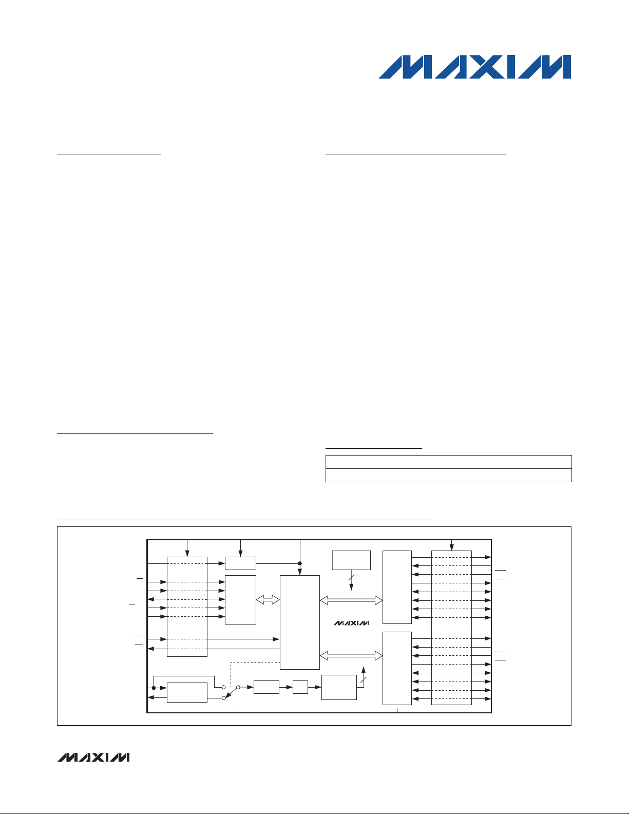
Functional Diagram
V
L
V
CC
Features
S 24Mbps (max) Baud Rate
S Integrated PLL and Divider
S 1.71V to 3.6V Supply Range
S High-Resolution Programmable Baud Rate
S SPI Up to 26MHz Clock Rate
S Fast Mode Plus I2C Up to 1MHz
S Automatic RTS_ and CTS_ Flow Control
S Automatic XON/XOFF Software Flow Control
S Special Character Detection
S 9-Bit Multidrop Mode Data Filtering
S SIR- and MIR-Compliant IrDASM Encoder/Decoder
S Flexible Logic Levels on the Controller and
Transceiver Interfaces
S Line Noise Indication
S 1FA Shutdown Current
S Two Timers Routed to GPIOs
S 8 Flexible GPIOs with 20mA Drive Capability
S Register Compatible with MAX3107, MAX3108,
MAX14830
S Small TQFN (5mm x 5mm) Package
Ordering Information
PART TEMP RANGE PIN-PACKAGE
MAX3109ETJ+
+Denotes a lead(Pb)-free/RoHS-compliant package.
*EP = Exposed pad.
V
18
-40NC to +85NC
V
EXT
32 TQFN-EP*
MAX3109
LDOEN
SPI/I2C
MOSI/A1
MISO/SDA
CS/A0
SCLK/SCL
RST
XOUT
LOGIC-LEVEL
TRANSLATION
IRQ
XIN
CRYSTAL
OSCILLATOR
LDO
SPI
AND
2
C
I
INTERFACE
DIVIDER
REGISTERS
AND
CONTROL
PLL
TRANSMITTER
SYNC
MAX3109
FRACTIONAL
BAUD-RATE
GENERATOR
2
UART0
LOGIC-LEVEL
TRANSLATION
UART1
2
DGNDAGND
TX0
RX0
CTS0
RTS0
GPIO0
GPIO1
GPIO2
GPIO3
TX1
RX1
CTS1
RTS1
GPIO4
GPIO5
GPIO6
GPIO7
IrDA is a service mark of Infrared Data Association Corporation.
_______________________________________________________________ Maxim Integrated Products 1
For pricing, delivery, and ordering information, please contact Maxim Direct at 1-888-629-4642,
or visit Maxim’s website at www.maxim-ic.com.
Page 2

Dual Serial UART with 128-Word FIFOs
TABLE OF CONTENTS
Absolute Maximum Ratings ...................................................................... 7
Package Thermal Characteristics.................................................................. 7
DC Electrical Characteristics .....................................................................7
AC Electrical Characteristics .................................................................... 10
Timing Diagrams ............................................................................. 12
MAX3109
Typical Operating Characteristics ................................................................ 13
Pin Configuration ............................................................................. 14
Pin Description ............................................................................... 14
Detailed Description........................................................................... 16
Receive and Transmit FIFOs...................................................................16
Transmitter Operation ........................................................................17
Receiver Operation ..........................................................................17
Line Noise Indication.........................................................................18
Clock Selection .............................................................................19
Crystal Oscillator .........................................................................19
External Clock Source .....................................................................19
PLL and Predivider ..........................................................................19
Fractional Baud-Rate Generators ...............................................................19
2x and 4x Rate Modes .......................................................................20
Low-Frequency Timer ........................................................................20
UART Clock to GPIO.........................................................................21
Multidrop Mode .............................................................................21
Auto Data Filtering in Multidrop Mode ...........................................................21
Auto Transceiver Direction Control ..............................................................21
Transmitter Triggering and Synchronization .......................................................21
Transmitter Synchronization .................................................................22
Intrachip and Interchip Synchronization........................................................22
Delayed Triggering........................................................................22
Trigger Accuracy .........................................................................22
Synchronization Accuracy ..................................................................23
Auto Transmitter Disable ...................................................................24
Echo Suppression ...........................................................................24
Auto Hardware Flow Control ...................................................................24
AutoRTS Control..........................................................................24
AutoCTS Control..........................................................................25
Auto Software (XON/XOFF) Flow Control .........................................................25
Receiver Flow Control .....................................................................25
Transmitter Flow Control....................................................................26
2 ______________________________________________________________________________________
Page 3

Dual Serial UART with 128-Word FIFOs
TABLE OF CONTENTS (continued)
FIFO Interrupt Triggering......................................................................26
Low-Power Standby Modes ...................................................................26
Forced-Sleep Mode .......................................................................26
Auto-Sleep Mode .........................................................................26
Multiple UARTs in Sleep Mode ..............................................................26
Shutdown Mode ..........................................................................27
Power-Up and IRQ ..........................................................................27
Interrupt Structure . . . . . . . . . . . . . . . . . . . . . . . . . . . . . . . . . . . . . . . . . . . . . . . . . . . . . . . . . . . . . . . . . . . . . . . . . . . 27
Interrupt Enabling.........................................................................27
Interrupt Clearing .........................................................................27
Register Map ................................................................................28
Detailed Register Descriptions................................................................... 29
Serial Controller Interface....................................................................... 57
SPI Interface ...............................................................................57
SPI Single-Cycle Access ...................................................................57
SPI Burst Access .........................................................................58
Fast Read Cycle..........................................................................58
I2C Interface ...............................................................................58
START, STOP, and Repeated START Conditions.................................................58
Slave Address ...........................................................................59
Bit Transfer ..............................................................................59
Single-Byte Write .........................................................................60
Burst Write ..............................................................................60
Single-Byte Read .........................................................................61
Burst Read ..............................................................................61
Acknowledge Bits ........................................................................62
Applications Information ........................................................................ 62
Startup and Initialization ......................................................................62
Low-Power Operation ........................................................................63
Interrupts and Polling ........................................................................63
Logic-Level Translation .......................................................................63
Power-Supply Sequencing ....................................................................64
Connector Sharing ..........................................................................64
RS-232 5x3 Application ......................................................................64
Typical Application Circuit ......................................................................65
Chip Information ..............................................................................65
Package Information........................................................................... 65
Revision History ..............................................................................66
MAX3109
_______________________________________________________________________________________ 3
Page 4

Dual Serial UART with 128-Word FIFOs
LIST OF FIGURES
Figure 1. I2C Timing Diagram.................................................................... 12
Figure 2. SPI Timing Diagram ................................................................... 12
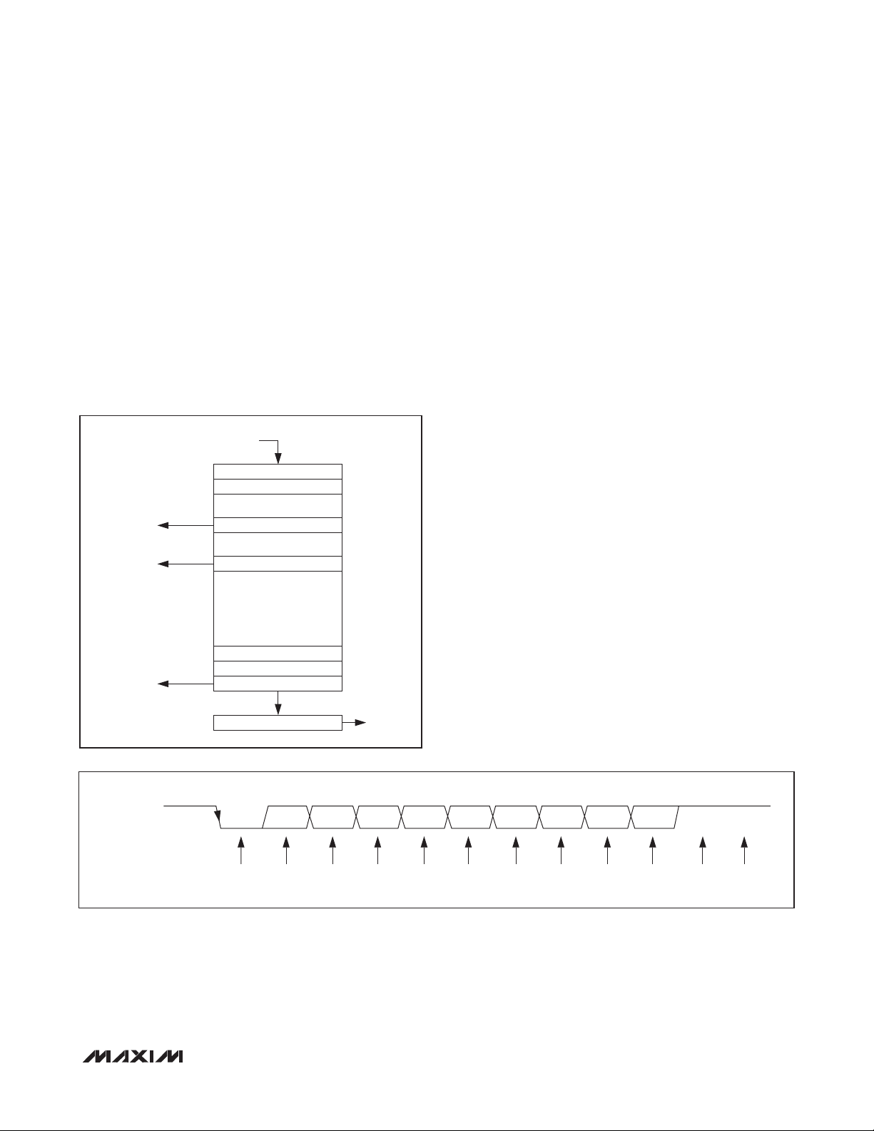
Figure 3. Transmit FIFO Signals .................................................................. 17
Figure 4. Receive Data Format................................................................... 17
Figure 5. Receive FIFO ........................................................................ 18
MAX3109
Figure 6. Midbit Sampling ...................................................................... 18
Figure 7. Clock Selection Diagram ................................................................ 19
Figure 8. 2x and 4x Baud Rates.................................................................. 20
Figure 9. GPIO_ Clock Pulse Generator............................................................ 20
Figure 10. Auto Transceiver Direction Control .......................................................22
Figure 11. Setup and Hold Times in Auto Transceiver Direction Control ................................... 22
Figure 12. Single Transmitter Trigger Accuracy ...................................................... 23
Figure 13. Multiple Transmitter Synchronization Accuracy.............................................. 23
Figure 14. Half-Duplex with Echo Suppression ...................................................... 24
Figure 15. Echo Suppression Timing .............................................................. 25
Figure 16. Simplified Interrupt Structure............................................................ 27
Figure 17. PLL Signal Path ......................................................................49
Figure 18. SPI Write Cycle ...................................................................... 57
Figure 19. SPI Ready Cycle ..................................................................... 57
Figure 20. SPI Fast Read Cycle .................................................................. 58
Figure 21. I2C START, STOP, and Repeated START Conditions ......................................... 59
Figure 22. Write Byte Sequence.................................................................. 60
Figure 23. Burst Write Sequence ................................................................. 60
Figure 24. Read Byte Sequence ................................................................. 61
Figure 25. Burst Read Sequence................................................................. 61
Figure 26. Acknowledge ....................................................................... 62
Figure 27. Startup and Initialization Flowchart . . . . . . . . . . . . . . . . . . . . . . . . . . . . . . . . . . . . . . . . . . . . . . . . . . . . . . . 62
Figure 28. Logic-Level Translation ................................................................ 63
Figure 29. Connector Sharing with a USB Transceiver ................................................ 64
Figure 30. RS-232 Application ................................................................... 64
Figure 31. RS-485 Half-Duplex Application ......................................................... 65
4 ______________________________________________________________________________________
Page 5

Dual Serial UART with 128-Word FIFOs
LIST OF TABLES
Table 1. StopBits Truth Table .................................................................... 40
Table 2. Lengthx Truth Table ....................................................................40
Table 3. SwFlow[3:0] Truth Table . . . . . . . . . . . . . . . . . . . . . . . . . . . . . . . . . . . . . . . . . . . . . . . . . . . . . . . . . . . . . . . . . 45
Table 4. PLLFactorx Selection Guide.............................................................. 49
Table 5. GloblComnd Command Descriptions ......................................................53
Table 6. Extended Mode Addressing (SPI Only) ..................................................... 53
Table 7. SPI Command Byte Configuration ......................................................... 57
Table 8. I2C Address Map ...................................................................... 59
LIST OF REGISTERS
Receive Hold Register (RHR).................................................................... 29
Transmit Hold Register (THR)....................................................................29
IRQ Enable Register (IRQEn) .................................................................... 30
Interrupt Status Register (ISR) ................................................................... 31
Line Status Interrupt Enable Register (LSRIntEn)..................................................... 32
Line Status Register (LSR) ...................................................................... 33
Special Character Interrupt Enable Register (SpclChrIntEn) ............................................ 34
Special Character Interrupt Register (SpclCharInt) ...................................................35
STS Interrupt Enable Register (STSIntEn) .......................................................... 36
Status Interrupt Register (STSInt) ................................................................. 37
MODE1 Register.............................................................................. 38
MODE2 Register .............................................................................39
Line Control Register (LCR) .....................................................................40
Receiver Timeout Register (RxTimeOut) ........................................................... 41
HDplxDelay Register .......................................................................... 41
IrDA Register ................................................................................ 42
Flow Level Register (FlowLvl)....................................................................42
FIFO Interrupt Trigger Level Register (FIFOTrgLvl) ................................................... 43
Transmit FIFO Level Register (TxFIFOLvl) ..........................................................43
Receive FIFO Level Register (RxFIFOLvl) ..........................................................43
Flow Control Register (FlowCtrl).................................................................. 44
XON1 Register ............................................................................... 45
XON2 Register ............................................................................... 46
XOFF1 Register .............................................................................. 46
XOFF2 Register .............................................................................. 47
GPIO Configuration Register (GPIOConfg) ......................................................... 47
MAX3109
_______________________________________________________________________________________ 5
Page 6

Dual Serial UART with 128-Word FIFOs
LIST OF REGISTERS (continued)
GPIO Data Register (GPIOData) .................................................................48
PLL Configuration Register (PLLConfig) ........................................................... 49
Baud-Rate Generator Configuration Register (BRGConfig) ............................................. 50
Baud-Rate Generator LSB Divisor Register (DIVLSB) ................................................. 50
Baud-Rate Generator MSB Divisor Register (DIVMSB) ................................................ 51
MAX3109
Clock Source Register (CLKSource) .............................................................. 51
Global IRQ Register (GlobalIRQ) ................................................................. 52
Global Command Register (GloblComnd) .......................................................... 53
Transmitter Synchronization Register (TxSynch) .....................................................54
Synchronization Delay Register 1 (SynchDelay1) .................................................... 55
Synchronization Delay Register 2 (SynchDelay2) .................................................... 55
Timer Register 1 (TIMER1) ......................................................................56
Timer Register 2 (TIMER2) ...................................................................... 56
Revision Identification Register (RevID) ............................................................56
6 ______________________________________________________________________________________
Page 7

Dual Serial UART with 128-Word FIFOs
ABSOLUTE MAXIMUM RATINGS
(Voltages referenced to AGND.)
VL, VCC, V
XOUT ........................................................ -0.3V to (VCC + 0.3V)
V
18 ......................
RST, IRQ, MOSI/A1, CS/A0, SCLK/SCL,
MISO/SDA, LDOEN, SPI/I2C .................... -0.3V to (VL + 0.3V)
TX_, RX_, CTS_, GPIO_ ........................... -0.3V to (V
DGND ................................................................... -0.3V to +0.3V
Stresses beyond those listed under “Absolute Maximum Ratings” may cause permanent damage to the device. These are stress ratings only, and functional
operation of the device at these or any other conditions beyond those indicated in the operational sections of the specifications is not implied. Exposure to absolute
maximum rating conditions for extended periods may affect device reliability.
, XIN ............................................... -0.3V to +4.0V
EXT
-0.3V to the lesser of (VCC + 0.3V) and 2.0V
EXT
+ 0.3V)
PACKAGE THERMAL CHARACTERISTICS (Note 1)
TQFN
Junction-to-Ambient Thermal Resistance (BJA) ...........47NC/W
Junction-to-Case Thermal Resistance (BJC) ...............1.7NC/W
Note 1: Package thermal resistances were obtained using the method described in JEDEC specification JESD51-7, using a four-
layer board. For detailed information on package thermal considerations, refer to www.maxim-ic.com/thermal-tutorial.
DC ELECTRICAL CHARACTERISTICS
(VCC = 1.71V to 3.6V, VL = 1.71V to 3.6V, V
VCC = 2.8V, VL = 1.8V, V
PARAMETER SYMBOL CONDITIONS MIN TYP MAX UNITS
Digital Interface Supply Voltage V
Analog Supply Voltage V
UART Interface Logic Supply
Voltage
Logic Supply Voltage V
CURRENT CONSUMPTION
VCC Supply Current I
V18 Input Power-Supply Current
in Shutdown Mode
VCC + VL + VA Shutdown Supply
Current
= 2.5V, TA = +25NC.) (Notes 2, 3)
EXT
V
I
18SHDN
I
SHDN
= 1.71V to 3.6V, TA = -40NC to +85NC, unless otherwise noted. Typical values are at
EXT
L
CC
EXT
CC
Internal PLL disabled and bypassed 1.71 3.6
Internal PLL enabled 2.35 3.6
18
1.8MHz crystal oscillator active, PLL
disabled, SPI/I2C interface idle, UART
interfaces idle, LDOEN = high
Baud rate = 1Mbps, 20MHz external clock,
SPI/I2C interface idle, PLL disabled, all
UARTs in loopback mode, LDOEN = low
RST = low, all inputs and outputs are idle
RST = low, MISO, SCLK, MOSI, SPI_I2C,
CS, LDOEN = 0/VL, CTSB0/1 = 0/V
CTSB0/1 = 0/V
Continuous Power Dissipation (TA = +70NC)
TQFN (derate 34.5mW/NC above +70NC) .............. 2758.6mW
Operating Temperature Range .......................... -40NC to +85NC
Maximum Junction Temperature .....................................+150NC
Storage Temperature Range ............................ -65NC to +150NC
Lead Temperature (soldering, 10s) ................................+300NC
Soldering Temperature (reflow) ......................................+260NC
1.71 3.6 V
1.71 3.6 V
1.65 1.95 V
500
500
100
0 1
EXT
EXT
,
V
FA
FA
FA
MAX3109
_______________________________________________________________________________________ 7
Page 8

Dual Serial UART with 128-Word FIFOs
DC ELECTRICAL CHARACTERISTICS (continued)
(VCC = 1.71V to 3.6V, VL = 1.71V to 3.6V, V
VCC = 2.8V, VL = 1.8V, V
= 2.5V, TA = +25NC.) (Notes 2, 3)
EXT
PARAMETER SYMBOL CONDITIONS MIN TYP MAX UNITS
V18 Input Power-Supply Current I
MAX3109
SCLK/SCL, MISO/SDA
MISO/SDA Output Logic-Low
Voltage in I2C Mode
MISO/SDA Output Low Voltage
in SPI Mode
MISO/SDA Output High Voltage
in SPI Mode
Input Logic-Low Voltage V
Input Logic-High Voltage V
Input Hysteresis V
Input Leakage Current I
Input Capacitance C
SPI/I2C, CS/A0, MOSI/A1 INPUTS
Input Logic-Low Voltage V
Input Logic-High Voltage V
Input Hysteresis V
Input Leakage Current I
Input Capacitance C
IRQ OUTPUT (OPEN DRAIN)
Output Logic-Low Voltage V
Output Leakage Current I
LDOEN AND RST INPUTS
Input Logic-Low Voltage V
Input Logic-High Voltage V
Input Hysteresis V
Input Leakage Current I
V
V
V
= 1.71V to 3.6V, TA = -40NC to +85NC, unless otherwise noted. Typical values are at
EXT
Baud rate = 1Mbps, 20MHz external clock,
18
PLL disabled, UART in loopback mode,
LDOEN = low (Note 4)
Sink current = 3mA, VL > 2V 0.4
OLI2C
OLSPI
OHSPI
HYST
HYST
OL
OL
HYST
Sink current = 3mA, VL < 2V
Sink current = 2mA 0.4 V
Source current = 2mA
SPI and I2C mode
IL
SPI and I2C mode
IH
VL -
0.4
0.7 x
V
SPI and I2C mode
VIN = 0 to VL, SPI and I2C mode -1 +1
IL
SPI and I2C mode 5 pF
IN
SPI and I2C mode
IL
SPI and I2C mode
IH
0.7 x
V
SPI and I2C mode 50 mV
VIN = 0 to VL, SPI and I2C mode -1 +1
IL
SPI and I2C mode 5 pF
IN
Sink current = 2mA 0.4 V
V
= 0 to VL, IRQ is not asserted
IRQ
IL
IH
IL
VIN = 0 to V
L
0.7 x
V
0.2 x
V
0.3 x
V
L
0.05 x
V
L
0.3 x
V
L
-1 +1
0.3 x
V
L
50 mV
-1 +1
4 mA
V
L
V
L
V
V
V
FA
L
V
V
FA
FA
L
V
V
FA
8 ______________________________________________________________________________________
Page 9

Dual Serial UART with 128-Word FIFOs
DC ELECTRICAL CHARACTERISTICS (continued)
(VCC = 1.71V to 3.6V, VL = 1.71V to 3.6V, V
VCC = 2.8V, VL = 1.8V, V
= 2.5V, TA = +25NC.) (Notes 2, 3)
EXT
PARAMETER SYMBOL CONDITIONS MIN TYP MAX UNITS
UART INTERFACE
RTS_, TX_ OUTPUTS
Output Logic-Low Voltage V
Output Logic-High Voltage V
Input Leakage Current I
Input Capacitance C
CTS_, RX_ INPUTS
Input Logic-Low Voltage V
Input Logic-High Voltage V
Input Hysteresis V
CTS_ Input Leakage Current
RX_ Pullup Current I
Input Capacitance C
GPIO_ INPUTS/OUTPUTS
Output Logic-Low Voltage V
Output Logic-High Voltage V
Input Logic-Low Voltage V
Input Logic-High Voltage V
Pulldown Current I
XIN
Input Logic-Low Voltage V
Input Logic-High Voltage V
Input Capacitance C
XOUT
Input Capacitance C
= 1.71V to 3.6V, TA = -40NC to +85NC, unless otherwise noted. Typical values are at
EXT
OL
OH
HYST
I
PU
Sink current = 2mA 0.4 V
Source current = 2mA
Output is three-stated, V
IL
High-Z mode 5 pF
IN
IL
IH
V
IL
IN
= 0 to V
CTS_
V
= 0V -7.5 -5.5 -3.5
RX_
EXT
Sink current = 20mA, push-pull or open-
OL
OH
IL
IH
PD
IL
IH
XIN
XOUT
drain output type, V
Sink current = 20mA, push-pull or opendrain output type, V
Source current = 5mA, push-pull output
type
GPIO_ is configured as an input 0.4 V
GPIO_ is configured as an input
V
= V
GPIO_
, GPIO_ is configured as an
EXT
input
EXT
EXT
> 2.3V
< 2.3V
RTS
= 0 to V
EXT
0.7 x
V
EXT
-1 +1
0.3 x
V
EXT
0.7 x
V
EXT
50 mV
-1 +1
5 pF
0.45
0.55
V
-
EXT
0.4
2/3 x
V
EXT
3.5 5.5 7.5
0.6 V
1.2 V
16 pF
16 pF
MAX3109
V
FA
V
V
FA
FA
V
V
V
FA
_______________________________________________________________________________________ 9
Page 10

Dual Serial UART with 128-Word FIFOs
AC ELECTRICAL CHARACTERISTICS
(VCC = 1.71V to 3.6V, VL = 1.71V to 3.6V, V
VCC = 2.8V, VL = 1.8V, V
PARAMETER SYMBOL CONDITIONS MIN TYP MAX UNITS
External Cystal Frequency f
External Clock Frequency f
External Clock Duty Cycle (Note 5) 45 55 %
MAX3109
Baud-Rate Generator Clock
Input Frequency
I2C BUS: TIMING CHARACTERISTICS (Figure 1)
SCL Clock Frequency f
Bus Free Time Between a STOP
and START Condition
Hold Time for START Condition
and Repeated START Condition
Low Period of the SCL Clock t
High Period of the SCL Clock t
Data Hold Time
Data Setup Time t
Setup Time for Repeated START
Condition
Rise Time of Incoming SDA and
SCL Signals
Fall Time of SDA and SCL
Signals
= 2.5V, TA = +25NC.) (Notes 2, 3)
EXT
XOSC
t
HD:STA
t
HD:DAT
SU:DAT
t
SU:STA
= 1.71V to 3.6V TA = -40NC to +85NC, unless otherwise noted. Typical values are at
EXT
1 4 MHz
CLK
f
REF
SCL
t
BUF
LOW
HIGH
t
R
t
F
(Note 5) 96 MHz
Standard mode 100
Fast mode plus 1000
Standard mode 4.7
Fast mode 1.3
Fast mode plus 0.5
Standard mode 4.0
Fast mode 0.6
Fast mode plus 0.26
Standard mode 4.7
Fast mode 1.3
Fast mode plus 0.5
Standard mode 4.0
Fast mode 0.6
Fast mode plus 0.26
Standard mode 0 0.9
Fast mode 0 0.9
Fast mode plus 0
Standard mode 250
Fast mode plus 50
Standard mode 4.7
Fast mode 0.2
Fast mode plus 0.26
Standard mode (0.3 x VL to 0.7 x VL)
(Note 6)
Fast mode (0.3 x VL to 0.7 x VL) (Note 6)
Fast mode plus 120
Standard mode (0.3 x VL to 0.7 x VL)
(Note 6)
Fast mode (0.3 x VL to 0.7 x VL) (Note 6)
Fast mode plus 120
0.5 35 MHz
20 +
0.1C
20 +
0.1C
20 +
0.1C
20 +
0.1C
B
B
B
B
1000
1000
300
300
kHzFast mode 400
Fs
Fs
Fs
Fs
Fs
nsFast mode 100
Fs
ns
ns
10 _____________________________________________________________________________________
Page 11

Dual Serial UART with 128-Word FIFOs
AC ELECTRICAL CHARACTERISTICS (continued)
(VCC = 1.71V to 3.6V, VL = 1.71V to 3.6V, V
VCC = 2.8V, VL = 1.8V, V
PARAMETER SYMBOL CONDITIONS MIN TYP MAX UNITS
Setup Time for STOP Condition t
Capacitive Load for SDA and
SCL
SCL and SDA I/O Capacitance C
Pulse Width of Spike Suppressed t
SPI BUS: TIMING CHARACTERISTICS (Figure 2)
SCLK Clock Period tCH+t
SCLK Pulse Width High t
SCLK Pulse Width Low t
CS Fall to SCLK Rise Time
MOSI Hold Time t
MOSI Setup Time t
Output Data Propagation Delay t
MISO Rise and Fall Times t
CS Hold Time
Note 2: All units are production tested at TA = +25NC. Specifications over temperature are guaranteed by design.
Note 3: Currents entering the IC are negative and currents exiting the IC are positive.
Note 4: When V18 is powered by an external voltage supply, it must have current capability above or equal to I18.
Note 5: Guaranteed by design; not production tested.
Note 6: CB is the total capacitance of either the clock or data line of the synchronous bus in pF.
= 2.5V, TA = +25NC.) (Notes 2, 3)
EXT
SU:STO
t
t
= 1.71V to 3.6V TA = -40NC to +85NC, unless otherwise noted. Typical values are at
EXT
Standard mode 4.7
Fast mode 0.6
Fast mode plus 0.26
Standard mode (Note 5) 400
C
B
Fast mode plus (Note 5) 550
(Note 5) 10 pF
I/O
SP
CL
CH
CL
CSS
DH
DS
DO
FT
CSH
38.4 ns
16 ns
16 ns
0 ns
3 ns
5 ns
30 ns
MAX3109
Fs
pFFast mode (Note 5) 400
50 ns
20 ns
10 ns
______________________________________________________________________________________ 11
Page 12
Dual Serial UART with 128-Word FIFOs
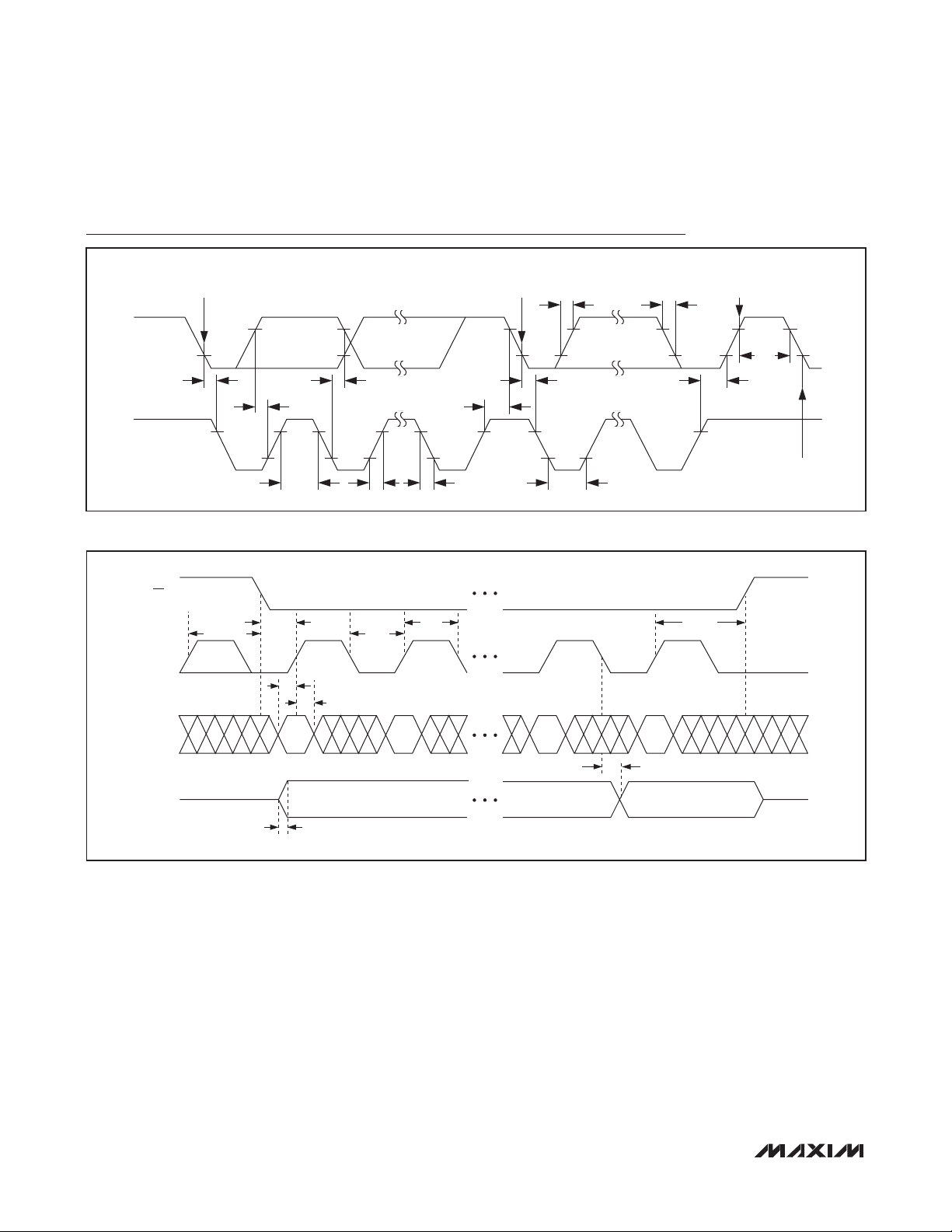
Timing Diagrams
START CONDITION
(S)
SDA
MAX3109
t
HD:STA
SCL
Figure 1. I2C Timing Diagram
CS
SCLK
t
CSH
t
CSS
t
HD:DAT
t
t
DS
t
SU:DAT
HIGH
t
DH
REPEATED START CONDITION
t
SU:STA
t
R
t
CL
t
F
t
CH
(Sr)
t
R
t
HD:STA
t
LOW
t
SU:STO
t
F
STOP CONDITION
t
CSH
(P)
t
BUF
START CONDITION
(S)
MOSI
t
DO
MISO
t
FT
Figure 2. SPI Timing Diagram
12 _____________________________________________________________________________________
Page 13
Dual Serial UART with 128-Word FIFOs
04
04
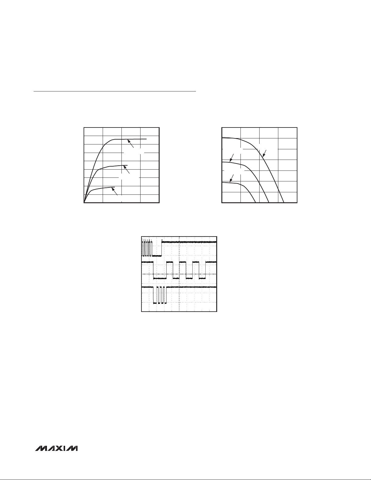
Typical Operating Characteristics
(VCC = 2.5V, VL = 2.5V, V
= 2.5V, V
EXT
= VL, UART1 in sleep mode, TA = +25°C unless otherwise noted.)
LDOEN
MAX3109
SINK CURRENT (OPEN DRAIN)
vs. GPIO_ OUTPUT LOW VOLTAGE
180
160
140
120
100
(mA)
SINK
80
I
60
40
20
0
V
EXT
V
EXT
= 1.71V
VOL (V)
V
EXT
= 2.5V
MAX3109 toc01
= 3.6V
321
TRANSMITTER SYNCHRONIZATION
10µs/div
(mA)
I
MAX3109 toc03
I2C MODE
SOURCE CURRENT (PUSH-PULL)
vs. GPIO_OUTPUT HIGH VOLTAGE
70
60
50
V
= 2.5V
EXT
40
30
V
= 1.8V
EXT
SOURCE
20
10
0
V
SCL
2V/div
0V
V
TX0
2V/div
115.2kBaud
0V
V
TX1
2V/div
460.8kBaud
0V
V
VOH (V)
EXT
= 3.3V
MAX3109 toc02
321
______________________________________________________________________________________ 13
Page 14
Dual Serial UART with 128-Word FIFOs
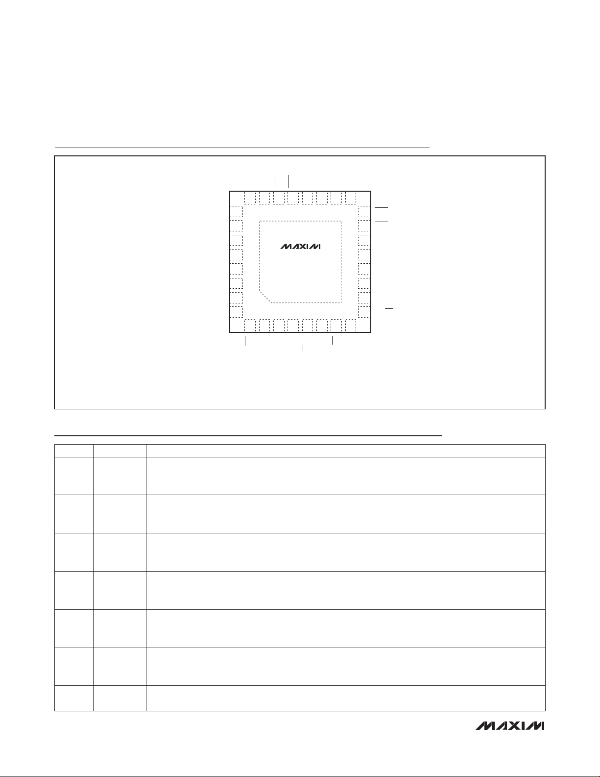
Pin Configuration
TOP VIEW
RTS1
GPIO2
RTS0
RX1
21
MAX3109
4567
GPIO7
CS/A0
SCLK/SCL
RX0
*EP
MOSI/A1
TX0
IRQ
TX1
17
16
CTS1
CTS0
15
14
GPIO5
GPIO1
13
12
GPIO4
GPIO0
11
10
DGND
9
SPI/I2C
8
L
V
MAX3109
V
EXT
XIN
XOUT
GPIO6
AGND
LDOEN
V
V
GPIO3
2324 22 20 19 18
25
26
27
28
29
30
31
18
CC
32
+
12
RST
MISO/SDA
3
TQFN
(5mm × 5mm)
*CONNECT EP TO AGND.
Pin Description
PIN NAME FUNCTION
Active-Low Reset Input. Drive RST low to force all of the UARTs into hardware reset mode. Driving RST
1
2 MISO/SDA
3 SCLK/SCL
4 GPIO7
RST
low also enables low-power shutdown mode. When RST is low, the internal V18 LDO is switched off,
even if the LDOEN input is kept high.
Serial-Data Output. When SPI/I2C is high, MISO/SDA functions as the SPI master input-slave output
(MISO). When SPI/I2C is low, MISO/SDA functions as the SDA, I2C serial-data input/output. MISO/SDA is
high impedance when RST is driven low or when the externally supplied V18 is powered off.
Serial-Clock Input. When SPI/I2C is high, SCLK/SCL functions as the SCLK SPI serial-clock input (up to
26 MHz). When SPI/I2C is low, SCLK/SCL functions as the SCL, I2C serial-clock input (up to 1MHz in
fast mode plus).
General-Purpose Input/Output 7. GPIO7 is user-programmable as an input or output (push-pull or open
drain) or an external event-driven interrupt source. GPIO7 has a weak pulldown resistor to DGND when
configured as an input.
Active-Low Chip-Select and Address 0 Input. When SPI/I2C is high, CS/A0 functions as the CS, SPI
5
CS/A0
active-low chip-select. When SPI/I2C is low, CS/A0 functions as the A0 I2C device address programming
input. Connect CS/A0 to DGND, VL, SCL, or SDA when SPI/I2C is low.
Serial-Data Input and Address 1 Input. When SPI/I2C is high, MOSI/A1 functions as the SPI master
6 MOSI/A1
output-slave input (MOSI). When SPI/I2C is low, MOSI/A1 functions as the A1 I2C device address
programming input. Connect MOSI/A1 to DGND, VL, SCL, or SDA when SPI/I2C is low.
7
IRQ
Active-Low Interrupt Open-Drain Output. IRQ is asserted when an interrupt is pending. IRQ is high
impedance when RST is driven low.
14 _____________________________________________________________________________________
Page 15

Dual Serial UART with 128-Word FIFOs
Pin Description (continued)
PIN NAME FUNCTION
8 V
9
10 DGND Digital Ground
11 GPIO0
12 GPIO4
13 GPIO1
14 GPIO5
15
16
17 TX1
18 TX0
19 RX0 Serial Receiving Data Input for UART0. RX0 has an internal weak pullup resistor to V
20 RX1 Serial Receiving Data Input for UART1. RX1 has an internal weak pullup resistor to V
21
22
23 GPIO2
24 GPIO3
25 V
26 XIN
L
SPI/I2C SPI Selector Input or Active-Low I2C. Drive SPI/I2C low to enable I2C. Drive SPI/I2C high to enable SPI.
CTS0 Active-Low Clear-to-Send Input for UART0. CTS0 is a flow-control status input.
CTS1 Active-Low Clear-to-Send Input for UART1. CTS1 is a flow-control status input.
RTS0
RTS1
EXT
Digital Interface Power Supply. VL powers the internal logic-level translators for RST, IRQ, MOSI/A1, CS/A0,
SCLK/SCL, MISO/SDA, LDOEN, and SPI/I2C. Bypass VL with a 0.1FF ceramic capacitor to DGND.
General-Purpose Input/Output 0. GPIO0 is user-programmable as an input or output (push-pull or open
drain) or an external event-driven interrupt source. GPIO0 has a weak pulldown resistor to DGND when
configured as an input. GPIO0 is the reference clock output when bit 7 of the TxSynch register is set to
high (see the UART Clock to GPIO section for more information).
General-Purpose Input/Output 4. GPIO4 is user-programmable as an input or output (push-pull or open
drain) or an external event-driven interrupt source. GPIO4 has a weak pulldown resistor to DGND when
configured as an input. GPIO4 is the reference clock output when bit 7 of the TxSynch register is set to
high (see the UART Clock to GPIO section for more information).
General-Purpose Input/Output 1. GPIO1 is user-programmable as an input or output (push-pull or open
drain) or an external event-driven interrupt source. GPIO1 has a weak pulldown resistor to DGND when
configured as an input. GPIO1 is the TIMER output when bit 7 of the TIMER2 register is set high.
General-Purpose Input/Output 5. GPIO5 is user-programmable as an input or output (push-pull or open
drain) or an external event-driven interrupt source. GPIO5 has a weak pulldown resistor to DGND when
configured as an input. GPIO5 is the TIMER output when bit 7 of the TIMER2 register is set high.
Serial Transmitting Data Output for UART1. TX1 is logic-high when RST is low or when the externally
supplied V18 is not powered.
Serial Transmitting Data Output for UART0. TX0 is logic-high when RST is low or when the externally
supplied V18 is not powered.
.
EXT
.
EXT
Active-Low Request-to-Send Output for UART0. RTS0 can be set high or low by programming the LCR
register. RTS0 is the UART system clock/fractional divider output when bit 7 of the CLKSource register is
set high. RTS0 is logic-high when RST is low or when the externally supplied V18 is not powered.
Active-Low Request-to-Send Output for UART1. RTS1 can be set high or low by programming the LCR
register. RTS1 is the UART system clock/fractional divider output when bit 7 of the CLKSource register is
set high. RTS1 is logic-high when RST is low or when the externally supplied V18 is not powered.
General-Purpose Input/Output 2. GPIO2 is user-programmable as input or output (push-pull or open
drain) or an external event-driven interrupt source. GPIO2 has a weak pulldown resistor to DGND when
configured as an input.
General-Purpose Input/Output 3. GPIO3 is user-programmable as input or output (push-pull or open
drain) or an external event-driven interrupt source. GPIO3 has a weak pulldown resistor to DGND when
configured as an input.
Transceiver Interface Power Supply. V
CTS_, and GPIO_. Bypass V
Crystal/Clock Input. When using an external crystal, connect one end of the crystal to XIN and the other
end to XOUT. When using an external clock source, drive XIN with the single-ended external clock.
with a 0.1FF ceramic capacitor to DGND.
EXT
powers the internal logic-level translators for RX_, TX_, RTS_,
EXT
MAX3109
______________________________________________________________________________________ 15
Page 16

Dual Serial UART with 128-Word FIFOs
Pin Description (continued)
PIN NAME FUNCTION
27 XOUT
28 GPIO6
MAX3109
29 AGND Analog Ground
30 LDOEN
31 V
32 V
— EP Exposed Pad. Connect EP to AGND. Do not use EP as the main AGND connection.
18
CC
Crystal Output. When using an external crystal, connect one end of the crystal to XOUT and the other
end to XIN. When using an external clock source, leave XOUT unconnected.
General-Purpose Input/Output 6. GPIO6 is user-programmable as input or output (push-pull or open
drain) or an external event-driven interrupt source. GPIO6 has a weak pulldown resistor to DGND when
configured as an input.
LDO Enable Input. Drive LDOEN high to enable the internal 1.8V LDO. Drive LDOEN low to disable the
internal LDO. Supply V
Internal 1.8V LDO Output and 1.8V Power-Supply Input. Bypass V18 with a 0.1FF ceramic capacitor to
DGND.
Analog Power Supply. VCC powers the PLL and internal LDO. Bypass VCC with a 0.1FF ceramic
capacitor to AGND.
with an external voltage source when LDOEN is low.
18
Detailed Description
The MAX3109 dual universal asynchronous receivertransmitter (UART) bridges an SPI/MICROWIREK or
I2C microprocessor bus to an asynchronous serial-data
communication link, such as RS-485, RS-232, or IrDA.
The MAX3109 is configured through 8-bit registers,
which are accessed through the SPI or I2C interface.
These registers are organized by related function as
shown in the Register Map section.
The host controller loads data into the Transmit Hold register (THR) through the SPI or I2C interface. This data is
automatically pushed into the transmit FIFOs, formatted,
and sent out at TX_. The MAX3109 adds START, STOP,
and parity bits to the data before transmitting the data
out at the selected baud rate. The clock configuration
registers determine the baud rates, clock source selection, clock frequency prescaling, and fractional baudrate generator settings for each UART.
The MAX3109 receivers detect a START bit as a highto-low transition on RX_. An internal clock samples this
data at 16 times the baud rate. The received data is
automatically placed in the receive FIFOs and can then
be read out by the host controller through the Receiver
Hold register (RHR).
The device features two identical UARTs that are completely independent except for the input clock. Text in
this data sheet references individual UART operation,
unless otherwise noted.
The MAX3109’s register set is compatible with the MAX3107.
Refer to Application Note 4938: Differences Between
Maxim's Advanced UART Devices for information on how
to transfer firmware from the MAX3107 to the MAX3109.
Receive and Transmit FIFOs
Each UART’s receiver and transmitter has a 128-worddeep FIFOs, reducing the number of intervals that the
host processor needs to dedicate for high-speed, highvolume data transfer to and from the device. As the data
rates of the asynchronous RX_/TX_ interfaces increase
and get closer to those of the host controller’s SPI/I2C
data rates, UART management and flow-control can
make up a significant portion of the host’s activity. By
increasing FIFO size, the host is interrupted less often
and can use data block transfers to and from the FIFOs.
FIFO trigger levels can generate interrupts to the host
controller, signaling that programmed FIFO fill levels
have been reached. The transmitter and receiver trigger
levels are programmed through the FIFOTrgLvl register
with a resolution of eight FIFO locations. The receive
FIFO trigger signals to the host either that the receive
FIFO has a defined number of words waiting to be read
out in a block or that a known number of vacant FIFO
locations are available and ready to be filled. The transmit FIFO trigger generates an interrupt when the transmit
FIFO fill level is above the programmed trigger level. The
host then knows to throttle data writing to the transmit
FIFO through THR.
The host can read out the number of words present in each of the FIFOs through the TxFIFOLvl and
RxFIFOLvl registers.
MICROWIRE is a trademark of National Semiconductor Corp.
16 _____________________________________________________________________________________
Page 17
Dual Serial UART with 128-Word FIFOs
The contents of the TxFIFO and RxFIFO are both cleared
when the MODE2[1]: FIFORst bit is set high
.Transmitter Operation
Figure 3 shows the structure of the transmitter with the
TxFIFO. The transmit FIFO can hold up to 128 words of
data that are added by writing to the THR register.
The current number of words in the TxFIFO can be read
out by the host controller through the TxFIFOLvl register. The transmit FIFO fill level can be programmed to
generate an interrupt when greater than or equal to a
programmed number of words are present in the TxFIFO
through the FIFOTrgLvl register. This TxFIFO interrupt
2
TRIGGER
LEVEL
EMPTY
C INTERFACE
CURRENT FILL LEVEL
THR
FIFOTrgLvl[3:0]
TRANSMIT FIFO
TRANSMITTER TX_
128
3
2
1
DATA FROM SPI/I
ISR[4]
TxFIFOLvl
ISR[5]
Figure 3. Transmit FIFO Signals
trigger level is selectable by the FIFOTrgLvl[3:0] bits.
MAX3109
When the transmit FIFO fill level increases to at least the
programmed trigger level, an interrupt is generated in
ISR[4]: TxTrigInt.
An interrupt is generated in ISR[5]: TFifoEmptyInt when
the transmit FIFO is empty. ISR[5] goes high when
the transmitter starts transmitting the last word in the
TxFIFO. An additional interrupt is generated in STSInt[7]:
TxEmptyInt when the transmitter completes transmitting
the last word.
To halt transmission, set the MODE1[1]: TxDisabl bit
high. After TxDisabl is set, the transmitter completes the
transmission of the current character and then ceases
transmission. Turn the transmitter off prior to enabling
auto software flow control and AutoRTS flow control.
The TX_ output logic can be inverted through the
IrDA[5]: TxInv bit. Unless otherwise noted, all transmitter
logic described in this data sheet assumes that TxInv is
set low.
Receiver Operation
The receiver expects the format of the data at RX_ to
be as shown in Figure 4. The quiescent logic state is
logic-high and the first bit (the START bit) is logic-low
(RxInv = 0). The 8-bit data word expected to be received
LSB first. The receiver samples the data near the midbit
instant (Figure 4). The received words and their associated errors are deposited into the receive FIFO. Errors
and status information are stored for every received word
(Figure 5). The host reads the data out of the receive
FIFO by reading RHR, which comes out oldest data first.
After a word is read out of RHR, LSR contains the status
information for that word.
RECEIVED DATA
MIDDATA
SAMPLING
NOTE: RxInv = 0.
Figure 4. Receive Data Format
START D0 D1 D2 D3 D4 D5 D6 D7 PARITY STOP STOP
______________________________________________________________________________________ 17
LSB
MSB
Page 18
Dual Serial UART with 128-Word FIFOs
The following three error conditions are checked for each
received word: parity error, frame error, and noise on the
line. Parity errors are detected by calculating either even
or odd parity of the received word as programmed by
register settings. Framing errors are detected when the
received data frame does not match the expected frame
format in length. Line noise is detected by checking the
logical congruency of the three samples taken of each
bit (Figure 6).
The receiver can be turned off by setting the MODE1[0]:
RxDisabl bit high. After this bit is set high, the MAX3109
turns the receiver off immediately following the current
word and does not receive any further data.
The RX_ input logic can be inverted by setting the
IrDA[4]: RxInv bit high. Unless otherwise noted, all
receiver logic described in this data sheet assumes that
RxInv is set low.
When operating in standard or 2x (i.e., not 4x) rate mode,
the MAX3109 checks that the binary logic level of the
three samples per received bit are identical. If any of
the three samples per received bit have differing logic
levels, then noise on the transmission line has affected
the received data and it is considered to be noisy. This
noise indication is reflected in the LSR[5]: RxNoise bit for
each received byte. Parity errors are another indication
of noise, but are not as sensitive.
ISR[3]
ISR[6]
OVERRUN
TRIGGER
TIMEOUT
LSR[1]
MAX3109
CURRENT FILL LEVEL
I2C/SPI INTERFACE
LSR[0]
LSR[5:2]
Figure 5. Receive FIFO
EMPTY
ERRORS
RECEIVER RX_
WORD ERROR 128
FIFOTrgLvl[7:4]
RECEIVE FIFO
RxFIFOLvl
RHR
RECEIVED
DATA
4
3
2
1
Line Noise Indication
ONE BIT PERIOD
RX_
BAUD
BLOCK
A
1
23456789
10 11
MAJORITY
CENTER
SAMPLER
12 13 14 15 16
Figure 6. Midbit Sampling
18 _____________________________________________________________________________________
Page 19
Dual Serial UART with 128-Word FIFOs
MAX3109
CrystalEn
XOUT
XIN
Figure 7. Clock Selection Diagram
CRYSTAL
OSCILLATOR
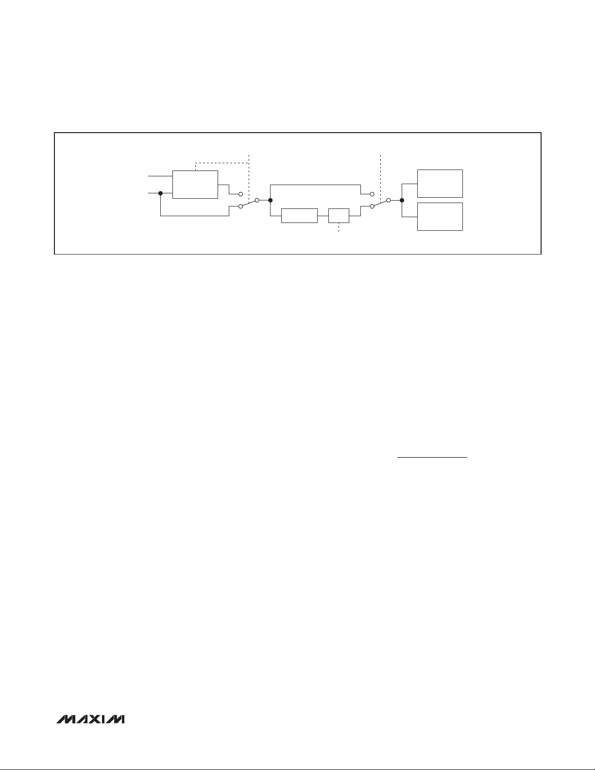
Clock Selection
The MAX3109 can be clocked by either an external
crystal or an external clock source. Figure 7 shows a
simplified diagram of the clock selection circuitry. When
the MAX3109 is clocked by a crystal, the STSInt[5]:
ClkReady bit indicates when the crystal oscillator has
reached steady state and the baud-rate generator is
ready for stable operation.
Each UART baud rate can be individually programmed
and both share the same reference clock input.
The baud-rate clock can be routed to the RTS_ output by
setting the CLKSource[7]: CLKtoRTS bit high. The clock
rate is 16x the baud rate in standard operating mode, 8x
the baud rate in 2x rate mode, and 4x the baud rate in 4x
rate mode. If the fractional portion of the baud-rate generator is used, the clock is not regular and exhibits jitter.
Crystal Oscillator
The MAX3109 is equipped with a crystal oscillator to provide high baud-rate accuracy and low power consumption. Set the CLKSource[1]: CrystalEn bit high to enable
and select the crystal oscillator. The on-chip crystal
oscillator has integrated load capacitances of 16pF in
both the XIN and XOUT pins. Connect only an external
crystal or ceramic oscillator between XIN and XOUT.
External Clock Source
Connect an external single-ended clock source to XIN
when not using the crystal oscillator. Leave XOUT unconnected. Set the CLKSource[1]: CrystalEn bit low to
select external clocking.
PLL and Predivider
The internal predivider and PLL allow for compatibility with
a wide range of external clock frequencies and baud rates.
The PLL can be configured to multiply the input clock
rate by a factor of 6, 48, 96, or 144 by the PLLConfig[7:6]
bits. The predivider is located between the input clock
and the PLL and allows division of the input clock by an
PLLBypass
FRACTIONAL
BAUD-RATE
GENERATOR 0
PLLDIVIDER
PLLEn
FRACTIONAL
BAUD-RATE
GENERATOR 1
integer factor between 1 and 63. This value is defined
by the PLLConfig[5:0] bits. See the PLLConfig register
description for more information. Use of the PLL requires
VCC to be higher than 2.35V.
Fractional Baud-Rate Generators
Each UART has an internal fractional baud-rate generator that provides a high degree of flexibility and high
resolution in baud-rate programming. The baud-rate
generator has a 16-bit integer divisor and a 4-bit word for
the fractional divisor. The fractional baud-rate generator
can be used either with the crystal oscillator or external
clock source.
The integer and fractional divisors are calculated by the
divisor, D:
×
f RateMode
REF
=
where f
D
is the reference frequency input to the baud-
REF
×
16 BaudRate
rate generator, RateMode is the rate mode multiplier (1x
default), BaudRate is the desired baud rate, and D is the
ideal divisor. f
must be less than 96MHz. RateMode
REF
is 1 in 1x rate mode, 2 in 2x rate mode, and 4 in 4x rate
mode.
The integer divisor portion, DIV, of the divisor, D, is
obtained by truncating D:
DIV = TRUNC(D)
DIV can be a maximum of 16 bits (65,535) wide and
is programmed into the two single-byte-wide registers
DIVMSB and DIVLSB. The minimum allowed value for
DIVLSB is 1.
The fractional portion of the divisor, FRACT, is a 4-bit
nibble that is programmed into BRGConfig[3:0]. The
maximum value is 15, allowing the divisor to be programmed with a resolution of 0.0625. FRACT is calculated as: FRACT = ROUND(16 x (D - DIV)).
______________________________________________________________________________________ 19
Page 20
Dual Serial UART with 128-Word FIFOs
The following is an example of how to calculate the divisor. It is based on a required baud rate of 190kbaud
and a reference input frequency of 28.23MHz and 1x
(default) rate mode.
The ideal divisor is calculated as:
D = 28,230,000/(16 x 190,000) = 9.286
hence DIV = 9.
MAX3109
FRACT = ROUND(16 x 0.286) = 5
so DIVMSB = 0x00, DIVLSB = 0x09, and BRGConfig[3:0]
= 0x05.
The resulting actual baud rate can be calculated as:
×
f RateMode
REF
BR
ACTUAL
=
×
16 D
ACTUAL
For this example:
D
ACTUAL
BR
= 9 + 5/16 = 9.3125, RateMode = 1, and
ACTUAL
= 28,230,000/(16 x 9.3125) = 189463 baud.
Thus, the actual baud rate is within 0.28% of the ideal
rate.
2x and 4x Rate Modes
To support higher baud rates than possible with standard operation using 16x sampling, the MAX3109 offers
2x and 4x rate modes. In these modes, the reference
clock rate only needs to be either 8x or 4x higher than the
baud rate, respectively. In 4x rate mode, each received
bit is only sampled once at the midbit instant instead of
the usual three samples to determine the logic value of
the received bit. This reduces the ability to detect line
noise on the received data in 4x rate mode. The 2x and
4x rate modes are selectable through BRGConfig[5:4].
Note that IrDA encoding and decoding does not operate
in 2x and 4x rate modes.
When 2x rate mode is selected, the actual baud rate is
twice the rate programmed into the baud-rate generator. If 4x rate mode is enabled, the actual baud rate on
the line is quadruple that of the programmed baud rate
(Figure 8).
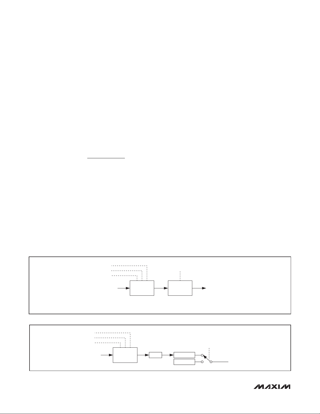
Low-Frequency Timer
Each UART has a general-purpose timer that can be
used to generate a low-frequency clock at a GPIO
output and can, for example, be used to drive external
LEDs. The low-frequency clock is a divided replica of the
given UART baud-rate clock. The timer for each UART
is internally routed to the respective GPIO_ output when
enabled by the TIMER2 register as follows:
U UART0: GPIO1
U UART1: GPIO5
The clock pulses at the GPIOs are generated at a rate
defined by the baud-rate generator and the timer divider
(Figure 9). The baud-rate generator clock frequency is
divided by (1024 x Timer[14:0]) to produce the GPIO_
clock, where Timer[14:0] is the 15-bit value programmed
into the TIMER1 and TIMER2 registers. The timer output
is 50% duty cycle clock.
DIVLSB
DIVMSB
FRACT
RATE
FRACTIONAL
RATE
GENERATOR
÷1024
f
REF
NOTE: IrDA DOES NOT WORK IN 2x AND 4x MODES.
Figure 8. 2x and 4x Baud Rates
DIVLSB
DIVMSB
FRACT
f
REF
Figure 9. GPIO_ Clock Pulse Generator
20 _____________________________________________________________________________________
FRACTIONAL
GENERATOR
BRGConfig[5:4]
1x, 2x, 4x RATE
MODES
÷TIMERx
GPIO_
BAUD RATE
TmrToGPIO
GPIO_
Page 21

Dual Serial UART with 128-Word FIFOs
UART Clock to GPIO
The MAX3109 reference clock can be routed to the
GPIO0 and/or GPIO4 outputs if a synchronous highfrequency clock is needed by another device. Enable
routing a UART clock to GPIO0 and/or GPIO4 in the
TxSynch register. This output clock could, for example,
be used to clock another UART device.
Multidrop Mode
In multidrop mode, also known as 9-bit mode, the data
word length is 8 bits and a 9th bit is used for distinguishing between an address word and a data word.
Multidrop mode is enabled by the MODE2[6]: MultiDrop
bit. The MultiDrop bit takes the place of the parity bit in
the data word structure. Parity checking is disabled and
an interrupt is generated in SpclCharInt[5]: MultiDropInt
when an address (9th bit is 1) is received while in multidrop mode.
It is up to the host processor to filter out the data intended
for its address. Alternatively, the auto data-filtering feature can be used to automatically filter out the data not
intended for the station’s specific 9-bit mode address.
Auto Data Filtering in Multidrop Mode
In multidrop mode, the MAX3109 can be configured
to automatically filter out data that is not meant for its
address. The address is user-definable either by programming a register value or a combination of a register
value and GPIO hardware inputs. Use either the entire
XOFF2 register or the XOFF2[7:4] bits in combination
with GPIO_ inputs to define the address.
Enable multidrop mode by setting the MODE2[6]:
MultiDrop bit high and enable auto data filtering by setting the MODE2[4]: SpecialChr bit high.
When using register bits in combination with GPIO_ inputs
to define the address, the MSB of the address is written
to the XOFF2[7:4] bits, while the LSBs of the address are
defined by the GPIOs. To enable this address-definition
method along with auto data filtering, set the FlowCtrl[2]:
GPIAddr bit high in addition to the MODE2[4]: SpecialChr
and MODE2[6]: MultiDrop bits. The GPIO_ inputs are
automatically read when the FlowCtrl[2]: GPIAddr bit is
set high, and the address is automatically updated on
logic changes to any GPIO pin.
When using auto data filtering, the MAX3109 checks
each received address against the programmed station
address. When an address is received that matches
the station’s address, received data is stored in the
RxFIFO. When an address is received that does not
match the station’s address, received data is discarded.
Addresses are not stored into the FIFO but an inter-
MAX3109
rupt is still generated in SpclCharInt[5]: MultiDropInt
upon receiving an address. An additional interrupt is
generated in SpclCharInt[3]: XOFF2Int when the station
address is received.
Auto Transceiver Direction Control
In some half-duplex communication systems, the transceiver’s transmitter must be turned off when data is
being received in order to not load the bus. This is the
case in half-duplex RS-485 communication. Similarly, in
full-duplex multidrop communication such as RS-485 or
RS-422 V.11, only one transmitter can be enabled at any
one time while the others must be disabled. The MAX3109
can automatically enable/disable a transceiver’s transmitter and/or receiver at the hardware level by controlling its
DE and RE pins. This feature relieves the host processor
of this time-critical task.
The RTS_ output is used to control the transceivers’
transmit-enable input and is automatically set high
when the MAX3109’s transmitter starts transmission.
This occurs as soon as data is present in the transmit
FIFO. Auto transceiver direction control is enabled by
the MODE1[4]: TrnscvCtrl bit. Figure 10 shows a typical
MAX3109 connection in an RS-485 application using the
auto transceiver direction control feature.
The RTS output can be set high in advance of TX_
transmission by a programmable time period called the
setup time (Figure 11). The setup time is programmed
by the HDplxDelay[7:4]: Setupx bits. Similarly, the RTS_
output can be held high for a programmable period
after the transmitter has completed transmission called
the hold time. The hold time is programmed by the
HDplxDelay[3:0] bits.
Transmitter Triggering and Synchronization
The MAX3109 allows synchronization of transmitters so
that selected UARTs start transmitting data when a trigger
command is received. Optional delays can also be programmed that delay the start of transmission after a trigger command is received. A UART’s transmitter can be
assigned one of 16 possible SPI/I2C trigger commands.
A trigger command is defined as any of the 16 special
values written into the GloblComnd register (see the
GloblComnd register description for more information).
When a byte is written into the GloblComnd register, the
UART select bit (U) is ignored by the MAX3109 and the
GloblComnd applies to both UARTs. Transmission is
initiated when the MAX3109 receives an assigned SPI/
I2C trigger command, the selected transmitter is initially
disabled, and data has been loaded into its TxFIFO.
______________________________________________________________________________________ 21
Page 22

Dual Serial UART with 128-Word FIFOs
TxFIFO
MAX3109
Figure 10. Auto Transceiver Direction Control
RTS_
TX_
MAX3109
RxFIFO
SETUP
DE
RE
RO
DI
D
MAX14840E
R
TRANSMITTER
AUTO
TRANSCEIVER
CONTROL
RECEIVER
FIRST CHARACTER LAST CHARACTER
TX_
RTS_
RX_
B
A
HOLD
Figure 11. Setup and Hold Times in Auto Transceiver Direction Control
Enable and configure transmitter synchronization with
the TxSynch register. Triggering and synchronization
requires that the transmitters are disabled before the
trigger is received. This can be done by setting the
MODE1[1]: TxDisabl bit high or by using the auto transmitter disable function (TxSynch[4] is logic 1).
Transmitter Synchronization
Synchronize multiple UARTs so that their transmitters
Interchip transmitter triggering synchronizes UARTs in
different MAX3109 devices. This type of synchronization is achievable in SPI mode only. Pull the CS input of
all the MAX3109 devices on the bus low during the SPI
master’s write trigger command so that the commands
are received by all UARTs on the shared SPI bus.
I2C protocol does not allow simultaneous addressing of
multiple devices.
start transmission simultaneously by assigning a common trigger command to the UARTs that should be
synchronized.
Intrachip and Interchip Synchronization
Intrachip transmitter triggering occurs when the two UARTs
A delay can be programmed to postpone the start of
transmission after receiving an assigned trigger command. Set the delay by programming the SynchDelay1
and SynchDelay2 registers.
in a MAX3109 device are triggered by one command. This
type of synchronization is supported in both SPI and I2C
modes, as the trigger commands are global commands
that are received by both UARTs simultaneously.
The delay between the time when the MAX3109 receives
a trigger command and the time when the associated transmitter starts transmission is made up of a fixed,
deterministic portion, and a variable, random component.
22 _____________________________________________________________________________________
Delayed Triggering
Trigger Accuracy
Page 23

Dual Serial UART with 128-Word FIFOs
56
Both portions of the delay are dependent on the UART’s
clock. When the fractional divider is not used, the intrinsic
trigger delay, t
, is bounded by the following limits:
TRIG
t
≤≤
UARTCLK UARTCLK
TRIG
where UARTCLK is the baud-rate divider output. The
reference point is the time when the trigger command is
received by the MAX3109. This occurs on the final (i.e.,
the 16th) SPI clock’s low-to-high transition (Figure 12).
SCLK
TX_
t
TRIG_MIN
t
TRIG_MAX
In I2C mode, this occurs on the final (i.e., the 8th) SCL
MAX3109
low-to-high transition.
When the fractional baud-rate generator is used, the
random portion is larger than one UART clock period.
Synchronization Accuracy
When synchronizing multiple UART transmitters, the output skew of the TX_ transmitter outputs is based on the
triggering delays of each UART (Figure 13). This skew
has a baud rate dependent component, similar to the
UNCERTAINTY
INTERVAL
Figure 12. Single Transmitter Trigger Accuracy
SCLK
TX0
TX1
Figure 13. Multiple Transmitter Synchronization Accuracy
t
TX0_MIN
t
TX0_MAX
t
TX1_MIN
t
TX1_MAX
t
TRIGSKEW
______________________________________________________________________________________ 23
Page 24

Dual Serial UART with 128-Word FIFOs
SF
65
trigger accuracy equation for a single transmitter output.
Calculate the TX_ transmitter output skew using the following equation:
t
TRIGSKEW
≤−
(UARTCLK) (UARTCLK)
where (UARTCLK)S is the fractional divider output clock
of the lower/slower baud rate UART, and (UARTCLK)
MAX3109
is the fractional divider output clock of the higher/faster
baud rate UART.
Auto Transmitter Disable
The MAX3109 allows automatic disabling of the transmitter. Enable auto transmitter disabling functionality by
setting the TxSynch[6]: TxAutoDis bit high. In this mode,
the MAX3109 disables the specified transmitter by setting the MODE1[1]: TxDisabl bit high after it completes
sending all the data in its TxFIFO. New data can then be
loaded into the TxFIFO. A disabled transmitter does not
send out data on the TX_ output when data is present in
its TxFIFO.
To enable transmission after a transmitter has been disabled automatically, either clear the TxAutoDis or toggle
the TxDisabl bit.
Echo Suppression
The MAX3109 can suppress echoed data that is sometimes found in half-duplex communication networks,
such as RS-485 and IrDA. If the transceiver’s receiver is
not turned off while the transceiver is transmitting, copies (echoes) of the transmitted data are received by the
UART. The MAX3109’s receiver can block the reception of this echoed data by enabling echo suppression.
Figure 14 shows a typical RS-485 application using the
echo suppression feature. Set the MODE2[7]: EchoSuprs
bit high to enable echo suppression.
The MAX3109 can also block echoes with a long round
trip delay by disabling the transceiver’s receiver with
the RTS_ output while the MAX3109 is transmitting. The
transmitter can be configured to remain enabled after
the end of the transmission for a programmable period
of time called the hold time delay (Figure 15). The hold
F
time delay is set by the HDplxDelay[3:0]: Holdx bits.
See the HDplxDelay description in the Detailed Register
Descriptions section for more information.
Echo suppression can operate simultaneously with auto
transceiver direction control.
Auto Hardware Flow Control
The MAX3109 is capable of auto hardware (RTS_ and
CTS_) flow control without the need for host proces-
sor intervention. When AutoRTS control is enabled,
the MAX3109 automatically controls the RTS_ handshake without the need for host processor intervention.
AutoCTS flow control separately turns the MAX3109’s
transmitter on and off based on the CTS_ input. AutoRTS
and AutoCTS flow control modes are independently
enabled by the FlowCtrl[1:0] bits.
AutoRTS Control
AutoRTS flow control ensures that the receive FIFO does
not overflow by signaling to the far-end UART to stop
data transmission. The MAX3109 does this automatically
by controlling the RTS_ output. AutoRTS flow control is
enabled by setting the FlowCtrl[0]: AutoRTS bit high.
The HALT and RESUME programmable values determine the threshold RxFIFO fill levels at which RTS_ is
asserted and deasserted. Set the HALT and RESUME
DE
RE
RO
DI
D
MAX14840E
R
TRANSMITTER
TxFIFO
ECHO
MAX3109
RxFIFO
Figure 14. Half-Duplex with Echo Suppression
24 _____________________________________________________________________________________
SUPPRESSION
RECEIVER
TX_
RTS_
RX_
B
A
Page 25

Dual Serial UART with 128-Word FIFOs
MAX3109
TX_
DI TO RO PROPAGATION DELAY
RX_
RTS_
Figure 15. Echo Suppression Timing
levels in the FlowLvl register. With differing HALT and
RESUME levels, hysteresis of the RxFIFO level can be
defined for RTS_ transitions.
When the RxFIFO is filled to a level higher than the HALT
level, the MAX3109 deasserts RTS_ and stops the farend UART from transmitting any additional data. RTS_
remains deasserted until the RxFIFO is emptied enough
so that the number of words falls to below the RESUME
level.
Interrupts are not generated when the HALT and
RESUME levels are reached. This allows the host controller to be completely disengaged from RTS_ flow
control management.
AutoCTS Control
When AutoCTS flow control is enabled, the UART automatically starts transmitting data when the CTS_ input
is logic-low and stops transmitting data when CTS_ is
logic-high. This frees the host processor from managing
this time-critical flow-control task. AutoCTS flow control is enabled by setting the FlowCtrl[1]: AutoCTS bit
high. The ISR[7]: CTSInt interrupt works normally during
AutoCTS flow control. Set the IRQEn[7]: CTSIntEn bit low
to disable routing of CTS_ interrupts to IRQ and ensure
that the host does not receive interrupts from CTS_
transitions. If CTS_ transitions from low to high during
transmission of a data word, the MAX3109 completes the
transmission of the current word and halts transmission
afterwards.
Turn the transmitter off by setting the MODE1[1]: TxDisabl
bit high before enabling AutoCTS control.
BIT
HOLD DELAYSTOP
Auto Software (XON/XOFF) Flow Control
When auto software flow control is enabled, the MAX3109
recognizes and/or sends predefined XON/XOFF characters to control the flow of data across the asynchronous
serial link. The XON character signifies that there is
enough room in the receive FIFO and transmission of
data should continue. The XOFF character signifies that
the receive FIFO is nearing overflow and that the transmission of data should stop. Auto software flow control
works autonomously and does not require host intervention, similar to auto hardware flow control. To reduce the
chance of receiving corrupted data that equals a singlebyte XON or XOFF character, the MAX3109 allows for
double-wide (16-bit) XON/XOFF characters. The XON
and XOFF characters are programmed into the XON1,
XON2 and XOFF1, XOFF2 registers.
The FlowCtrl[7:3] bits are used for enabling and configuring auto software flow control. An interrupt is generated
in ISR[1]: SpCharInt whenever an XON or XOFF character is received and details are stored in the SpclCharInt
register. Set the IRQEn[1]: SpclChrIEn bit low to disable
routing of the interrupt to IRQ.
Software flow control consists of transmit flow control
and receive flow control, which operate independently
of each other.
Receiver Flow Control
When auto receive flow control is enabled by the
FlowCtrl[7:6] bits, the MAX3109 automatically controls
the transmission of data by the far-end UART by sending XOFF and XON control characters. The HALT and
RESUME levels determine the threshold RxFIFO fill levels
______________________________________________________________________________________ 25
Page 26

Dual Serial UART with 128-Word FIFOs
at which the XOFF and XON characters are sent. HALT
and RESUME are programmed in the FlowLvl register.
With differing HALT and RESUME levels, hysteresis can
be defined in the RxFIFO fill level for the receiver flow
control activity.
When the RxFIFO is filled to a level higher than the HALT
level, the MAX3109 sends an XOFF character to stop
data transmission. An XON character is sent when the
MAX3109
RxFIFO is emptied enough so that the number of words
falls to below the RESUME level.
If double-wide (16-bit) XON/XOFF characters are selected by setting the FlowCtrl[7:6] bits to 11, then XON1/
XOFF1 are transmitted before XON2/XOFF2 whenever a
control character is transmitted.
Transmitter Flow Control
If auto transmit control is enabled by the FlowCtrl[5:4]
bits, the receiver compares all received words with the
XOFF and XON characters. When an XOFF character
is received, the MAX3109 halts the transmitter from
sending further data following any currently transmitting
word. The receiver is not affected and continues receiving. Upon receiving an XON character, the transmitter
restarts sending data. The received XON and XOFF
characters are filtered out and are not stored into the
receive FIFO. An interrupt is not generated.
If double-wide (16-bit) XON/XOFF characters are selected by setting the FlowCtrl[5:4] bits to 11, then a character matching XON1/XOFF1 must be received before
a character matching XON2/XOFF2 in order to be interpreted as a control character.
Turn the transmitter off by setting the MODE1[1]: TxDisabl
bit high before enabling software transmitter flow control.
FIFO Interrupt Triggering
Receive and transmit FIFO fill-dependent interrupts are
generated if FIFO trigger levels are defined. When the
number of words in the FIFOs reach or exceed a trigger level programmed in the FIFOTrgLvl register, an
interrupt is generated in ISR[3] or ISR[4]. The interrupt
trigger levels operate independently from the HALT and
RESUME flow control levels in AutoRTS or auto software
flow control modes.
The FIFO interrupt triggering can be used, for example,
for a block data transfer. The trigger level interrupt gives
the host an indication that a given block size of data is
available for reading in the receive FIFO or available for
transfer to the transmit FIFO. If the HALT and RESUME
levels are outside of this range, then the UART continues
to transmit or receive data during the block read/write
operations for uninterrupted data transmission on the
bus.
Low-Power Standby Modes
The MAX3109 has sleep and shutdown modes that
reduce power consumption during periods of inactivity.
In both sleep and shutdown modes, the UART disables
specific functional blocks to reduce power consumption.
After sleep or shutdown mode is exited, the internal clock
starts up and a period of time is needed for clock stabilization. The STSInt[5]: ClkReady bit indicates when the
clocks are stable. When an external clock source is used,
the ClkReady bit does not indicate clock stability.
Forced-Sleep Mode
In forced-sleep mode, all UART-related on-chip clocking is stopped. The following blocks are inactive: the
crystal oscillator, the PLL, the predivider, the receiver,
and the transmitter. The I2C/SPI interface and the registers remain active and the host controller can access
them. To force the MAX3109 to enter sleep mode, set the
MODE1[5]: ForcedSleep bit high. To exit forced-sleep
mode, set the ForcedSleep bit low.
Auto-Sleep Mode
The MAX3109 can be configured to operate in auto-sleep
mode by setting the MODE1[6]: AutoSleep bit high. In
auto-sleep mode, the MAX3109 automatically enters
sleep mode when all the following conditions are met:
• BothFIFOsareempty.
• TherearenopendingIRQ interrupts.
• There is no activity on any input pins for a period
equal to 65,536 UART character lengths.
The same blocks are inactive when the UART is in autosleep mode as in forced-sleep mode.
The MAX3109 exits auto-sleep mode as soon as activity
is detected on any of the GPIO_, RX_, or CTS_ inputs.
To manually exit auto-sleep mode, set the MODE1[6]:
AutoSleep bit low.
Multiple UARTs in Sleep Mode
The MAX3109's two UARTs enter and exit sleep mode
separately. When only one UART is in sleep mode, the
device stops routing the clock to this UART, reducing
power consumption. All other clocking circuitry remains
active if the other UART is still active. If both UARTs are
in sleep mode, the clocking circuitry is switched off, further reducing power consumption.
26 _____________________________________________________________________________________
Page 27

Dual Serial UART with 128-Word FIFOs
Shutdown Mode
Drive the RST input to logic-low to enter shutdown mode.
Shutdown mode consumes less than 1FA. In shutdown
mode, all the MAX3109 circuitry is completely off. This
includes the I2C/SPI interface, the registers, the FIFOs,
and the clocking circuitry.
When the RST input transitions from low to high, the
MAX3109 exits shutdown mode and a hardware reset
is initiated. The chip initialization is complete when the
I2C/SPI controller is able to read out known register contents from the MAX3109. This could, for example, be the
DIVLSB register.
The MAX3109 needs to be reprogrammed following a
shutdown.
Power-Up and IRQ
The IRQ output only operates when all supplies are
active. IRQ operates as a hardware active-low interrupt
output; IRQ is asserted when an interrupt is pending. An
IRQ interrupt is only possible during normal operation
if at least one of the interrupt enable bits in the IRQEn
register is set.
In polled mode, any register with a known reset value
can be polled to check whether the MAX3109 is ready for
operation. If the controller gets a valid response from the
polled register, then the MAX3109 is ready for operation.
Interrupt Structure
MAX3109
Figure 16 shows the structure of the interrupt. There are
four interrupt source registers: ISR, LSR, STSInt, and
SpclCharInt. The interrupt sources are divided into toplevel and low-level interrupts. The top-level interrupts
typically occur more often and can be read out by the
host controller directly through ISR. The low-level interrupts typically occur less often and their specific source
can be read out by the host controller through LSR,
STSInt, or SpclCharInt. The three LSBs of ISR point to
the low-level interrupt registers that contain the details of
the interrupt source.
Interrupt Enabling
Every interrupt bit of the four interrupt registers can be
enabled or masked through an associated interrupt
enable register bit. These are the IRQEn, LSRIntEn,
SpclChrIntEn, and STSIntEn registers. By default, all
interrupts are masked.
Interrupt Clearing
When an interrupt is pending (i.e., IRQ is asserted) and
ISR is read, both the ISR bits are cleared and the IRQ
output is deasserted. Low-level interrupt information
does not reassert IRQ for the same interrupt, but remains
stored in the low-level interrupt registers until each is
separately cleared. SpclCharInt and STSInt are clearon-read (COR). The LSR bits are only cleared when the
source of the interrupt is removed, not when LSR is read.
0 0 0 0 0 0 IRQ1 IRQ0
8
ISR
7 6 5 4 3 2 1 0
8
STSInt
6 5 4 3 2 1 0
7
Figure 16. Simplified Interrupt Structure
______________________________________________________________________________________ 27
[1]
[0]
GlobalIRQ
8
6 5 4 3 2 1 0
7
LOW-LEVEL INTERRUPTS
7
IRQ
ISR
8
SpclCharInt
6 5 4 3 2 1 0
TOP-LEVEL INTERRUPTS
8
LSR
6 5 4 3 2 1 0
7
Page 28

Dual Serial UART with 128-Word FIFOs
Register Map
(Note: All default reset values are 0x00, unless otherwise noted. All registers are R/W, unless otherwise noted.)
REGISTER ADDR BIT 7 BIT 6 BIT 5 BIT 4 BIT 3 BIT 2 BIT 1 BIT 0
FIFO DATA
1
RHR
1
THR
INTERRUPTS
IRQEn 0x01 CTSIEn RxEmtyIEn TFifoEmtyIEn TxTrgIEn RxTrgIEn STSIEn SpChrIEn LSRErrIEn
1, 2
ISR
MAX3109
LSRIntEn 0x03 — — NoiseIntEn RBreakIEn FrameErrIEn ParityIEn ROverrIEn RTimoutIEn
1, 2
LSR
SpclChrIntEn 0x05 — — MltDrpIntEn BREAKIntEn XOFF2IntEn XOFF1IntEn XON2IntEn XON1IntEn
SpclCharInt
STSIntEn
STSInt
1
3
1, 2, 3
UART MODES
MODE1 0x09 IRQSel AutoSleep ForcedSleep TrnscvCtrl RTSHiZ TxHiZ TxDisabl RxDisabl
MODE2 0x0A EchoSuprs MultiDrop Loopback SpecialChr RFifoEmptyInv RxTrgInv FIFORst RST
2
LCR
RxTimeOut 0x0C TimOut7 TimOut6 TimOut5 TimOut4 TimOut3 TimOut2 TimOut1 TimOut0
HDplxDelay 0x0D Setup3 Setup2 Setup1 Setup0 Hold3 Hold2 Hold1 Hold0
IrDA 0x0E — — TxInv RxInv MIR — SIR IrDAEn
FIFOs CONTROL
FlowLvl 0x0F Resume3 Resume2 Resume1 Resume0 Halt3 Halt2 Halt1 Halt0
FIFOTrgLvl
TxFIFOLvl
RxFIFOLvl
2
1
1
FLOW CONTROL
FlowCtrl 0x13 SwFlow3 SwFlow2 SwFlow1 SwFlow0 SwFlowEn GPIAddr AutoCTS AutoRTS
XON1 0x14 Bit7 Bit6 Bit5 Bit4 Bit3 Bit2 Bit1 Bit0
XON2 0x15 Bit7 Bit6 Bit5 Bit4 Bit3 Bit2 Bit1 Bit0
XOFF1 0x16 Bit7 Bit6 Bit5 Bit4 Bit3 Bit2 Bit1 Bit0
XOFF2 0x17 Bit7 Bit6 Bit5 Bit4 Bit3 Bit2 Bit1 Bit0
GPIOs
GPIOConfg
GPIOData
CLOCK CONFIGURATION
PLLConfig
BRGConfig 0x1B — — 4xMode 2xMode FRACT3 FRACT2 FRACT1 FRACT0
DIVLSB
DIVMSB 0x1D Div15 Div14 Div13 Div12 Div11 Div10 Div9 Div8
CLKSource
GLOBAL REGISTERS
GlobalIRQ
GloblComnd
SYNCHRONIZATION
TxSynch
SynchDelay1
SynchDelay2
TIMER REGISTERS
TIMER1
TIMER2
REVISION
RevID
1
Denotes nonread/write mode: RHR = R, THR = W, ISR = COR, LSR = R, SpclCharInt = COR, STSInt = R/COR, TxFIFOLvl = R,
3
3
2, 4
2
2, 4
1, 2
1
5
5
5
5
5
1, 2, 5
RxFIFOLvl = R, GlobalIRQ = R, GloblComnd = W, RevID = R.
2
Denotes nonzero default reset value: ISR = 0x60, LCR = 0x05, FIFOTrgLvl = 0xFF, PLLConfig = 0x01, DIVLSB = 0x01,
CLKSource = 0x18, GlobalIRQ = 0x03, RevID = 0xC1.
3
Each UART has four individually assigned GPIO outputs as follows: UART0: GPIO0–GPIO3, UART1: GPIO4–GPIO7.
4
Denotes a register that can only be programmed by accessing UART0.
5
Denotes a register that can only be directly addressed in I2C mode. Use extended addressing when operating in SPI mode.
0x00 RData7 RData6 RData5 RData4 RData3 RData2 RData1 RData0
0x00 TData7 TData6 TData5 TData4 TData3 TData2 TData1 TData0
0x02 CTSInt RxEmptyInt TFifoEmptyInt TxTrgInt RxTrigInt STSInt SpCharInt LSRErrInt
0x04
CTSbit
— RxNoise RxBreak FrameErr RxParityErr RxOverrun RTimeout
0x06 — — MultiDropInt BREAKInt XOFF2Int XOFF1Int XON2Int XON1Int
0x07 TxEmptyIntEn SleepIntEn ClkRdyIntEn — GPI3IntEn GPI2IntEn GPI1IntEn GPI0IntEn
0x08 TxEmptyInt SleepInt ClkReady — GPI3Int GPI2Int GPI1Int GPI0Int
0x0B
RTSbit
TxBreak ForceParity EvenParity ParityEn StopBits Length1 Length0
0x10 RxTrig3 RxTrig2 RxTrig1 RxTrig0 TxTrig3 TxTrig2 TxTrig1 TxTrig0
0x11 TxFL7 TxFL6 TxFL5 TxFL4 TxFL3 TxFL2 TxFL1 TxFL0
0x12 RxFL7 RxFL6 RxFL5 RxFL4 RxFL3 RxFL2 RxFL1 RxFL0
0x18 GP3OD GP2OD GP1OD GP0OD GP3Out GP2Out GP1Out GP0Out
0x19 GPI3Dat GPI2Dat GPI1Dat GPI0Dat GPO3Dat GPO2Dat GPO1Dat GPO0Dat
0x1A PLLFactor1 PLLFactor0 PreDiv5 PreDiv4 PreDiv3 PreDiv2 PreDiv1 PreDiv0
0x1C Div7 Div6 Div5 Div4 Div3 Div2 Div1 Div0
0x1E CLKtoRTS — — — PLLBypass PLLEn CystalEn —
0x1F 0 0 0 0 0 0
IRQ1 IRQ0
0x1F GlbCom7 GlbCom6 GlbCom5 GlbCom4 GlbCom3 GlbCom2 GlbCom1 GlbCom0
0x20 CLKtoGPIO TxAutoDis TrigDelay SynchEn TrigSel3 TrigSel2 TrigSel1 TrigSel0
0x21 SDelay7 SDelay6 SDelay5 SDelay4 SDelay3 SDelay2 SDelay1 SDelay0
0x22 SDelay15 SDelay14 SDelay13 SDelay12 SDelay11 SDelay10 SDelay9 SDelay8
0x23 Timer7 Timer6 Timer5 Timer4 Timer3 Timer2 Timer1 Timer0
0x24 TmrToGPIO Timer14 Timer13 Timer12 Timer11 Timer10 Timer9 Timer8
0x25 1 1 0 0 0 0 0 1
28 _____________________________________________________________________________________
Page 29

Dual Serial UART with 128-Word FIFOs
Detailed Register Descriptions
The MAX3109 has 8-bit-wide registers. When using SPI control, the extended register location (0x20 through 0x25) can
only be accessed by first enabling extended read/writing through GloblComnd. Each UART has an exclusive set of
registers. Select a UART to write to by setting the U bit of the command byte in SPI mode or the unique I2C address
in I2C mode (see the Serial Controller Interface section for more information).
Receive Hold Register (RHR)
ADDRESS: 0x00
MODE: R
BIT 7 6 5 4 3 2 1 0
NAME
RESET
Bits 7–0: RDatax
The RHR is the bottom of the receive FIFO and is the register used for reading data out of the receive FIFO. It contains
the oldest (first received) character in the receive FIFO. RHR[0] is the LSB of the character received at the RX_ input.
It is the first data bit of the serial-data word received by the receiver. Reading RHR removes the read word from the
receive FIFO, clearing space for more data to be received.
Transmit Hold Register (THR)
ADDRESS: 0x00
MODE: W
BIT 7 6 5 4 3 2 1 0
NAME
RESET
RData7 RData6 RData5 RData4 RData3 RData2 RData1 RData0
0 0 0 0 0 0 0 0
TData7 TData6 TData5 TData4 TData3 TData2 TData1 TData0
0 0 0 0 0 0 0 0
MAX3109
Bits 7–0: TDatax
The THR is the register that the host controller writes data to for subsequent UART transmission. This data is deposited in the transmit FIFO. THR[0] is the LSB. It is the first data bit of the serial-data word that the transmitter sends out,
immediately after the START bit.
______________________________________________________________________________________ 29
Page 30

Dual Serial UART with 128-Word FIFOs
IRQ Enable Register (IRQEn)
ADDRESS: 0x01
MODE: R/W
BIT 7 6 5 4 3 2 1 0
NAME
RESET
MAX3109
The IRQEn register is used to enable the IRQ physical interrupt. Any of the eight ISR interrupt sources can be enabled
to generate an interrupt on IRQ. The IRQEn bits only influence the IRQ output and do not have any effect on the ISR
contents or behavior. Every one of the IRQEn bits operates on a corresponding ISR bit.
Bit 7: CTSIEn
The CTSIEn bit enables IRQ interrupt generation when the CTSInt interrupt is set in ISR[7]. Set CTSIEn low to disable
IRQ generation from CTSInt.
Bit 6: RxEmtyIEn
The RxEmtyIEn bit enables IRQ interrupt generation when the RxEmptyInt interrupt is set in ISR[6]. Set RxEmtyIEn low
to disable IRQ generation from RxEmptyInt.
Bit 5: TFifoEmtyIEn
The TFifoEmtyIEn bit enables IRQ interrupt generation when the TFifoEmptyInt interrupt is set in ISR[5]. Set TFifoEmtyIEn
low to disable IRQ generation from TFifoEmptyInt.
Bit 4: TxTrgIEn
The TxTrgIEn bit enables IRQ interrupt generation when the TxTrigInt interrupt is set in ISR[4]. Set TxTrgIEn low to
disable IRQ generation from TxTrigInt.
Bit 3: RxTrgIEn
The RxTrgIEn bit enables IRQ interrupt generation when the RxTrigInt interrupt is set in ISR[3]. Set RxTrgIEn low to
disable IRQ generation from RxTrigInt.
Bit 2: STSIEn
The STSIEn bit enables IRQ interrupt generation when the STSInt interrupt is set in ISR[2]. Set STSIEn low to disable
IRQ generation from STSInt.
Bit 1: SpChrIEn
The SpChrIEn bit enables IRQ interrupt generation when the SpCharInt interrupt is set in ISR[1]. Set SpChrIEn low to
disable IRQ generation from SpCharInt.
Bit 0: LSRErrIEn
The LSRErrIEn bit enables IRQ interrupt generation when the LSRErrInt interrupt is set in ISR[0]. Set LSRErrIEn low to
disable IRQ generation from LSRErrInt.
CTSIEn RxEmtyIEn TFifoEmtyIEn TxTrgIEn RxTrgIEn STSIEn SpChrIEn LSRErrIEn
0 0 0 0 0 0 0 0
30 _____________________________________________________________________________________
Page 31

Dual Serial UART with 128-Word FIFOs
Interrupt Status Register (ISR)
ADDRESS: 0x02
MODE: COR
BIT 7 6 5 4 3 2 1 0
NAME
RESET
The Interrupt Status register provides an overview of all interrupts generated by the MAX3109. Both the interrupt bits
and any pending interrupts on IRQ are cleared after reading ISR. When the MAX3109 is operated in polled mode, ISR
can be polled to establish the UART’s status. In interrupt-driven mode, IRQ interrupts are enabled by the appropriate
IRQEn bits. The ISR contents either give direct information on the cause for the interrupt or point to other registers that
contain more detailed information.
Bit 7: CTSInt
The CTSInt interrupt is generated when a logic state transition occurs at the CTS_ input. CTSInt is cleared after ISR is
read. The current logic state of the CTS_ input can be read out through the LSR[7]: CTSbit bit.
Bit 6: RxEmptyInt
The RxEmptyInt interrupt is generated when the receive FIFO is empty. RxEmptyInt is cleared after ISR is read. Its
meaning can be inverted by the MODE2[3]: RFifoEmptyInv bit.
Bit 5: TFifoEmptyInt
The TFifoEmptyInt interrupt is generated when the transmit FIFO is empty and the transmitter is transmitting the last
character. Use STSInt[7]: TxEmptyInt to determine when the last character has completed transmission. TFifoEmptyInt
is cleared after ISR is read.
Bit 4: TxTrigInt
The TxTrigInt interrupt is generated when the number of characters in the transmit FIFO is equal to or greater than the
transmit FIFO trigger level defined in FIFOTrgLvl[3:0]. TxTrigInt is cleared when the transmit FIFO level falls below the
trigger level or after ISR is read. TxTrigInt can be used as a warning that the transmit FIFO is nearing overflow.
Bit 3: RxTrigInt
The RxTrigInt interrupt is generated when the receive FIFO fill level reaches the receive FIFO trigger level defined in
FIFOTrgLvl[7:4]. RxTrigInt can be used as an indication that the receive FIFO is nearing overrun. It can also be used
to report that a known number of words are available that can be read out in one block. The meaning of RxTrigInt can
be inverted by the MODE2[2]: RxTrigInv bit. RxTrigInt is cleared after ISR is read.
Bit 2: STSInt
The STSInt interrupt is generated when any interrupt in the STSInt register that is enabled by a STSIntEn bit is high.
STSInt is cleared after ISR is read, but the interrupt in STSInt that caused this interrupt remains set. See the STSInt
register description for details about this interrupt.
Bit 1: SpCharInt
The SpCharInt interrupt is generated when a special character is received, a line break is detected, or an address
character is received in multidrop mode. SpCharInt is cleared after ISR is read, but the interrupt in SpclCharInt that
caused this interrupt remains set. See the SpclCharInt register description for details about this interrupt.
Bit 0: LSRErrInt
The LSRErrInt interrupt is generated when any interrupts in LSR that are enabled by corresponding bits in LSRIntEn
are set. This bit is cleared after ISR is read. See the LSR register description for details about this interrupt.
CTSInt RxEmptyInt TFifoEmptyInt TxTrigInt RxTrigInt STSInt SpCharInt LSRErrInt
0 1 1 0 0 0 0 0
MAX3109
______________________________________________________________________________________ 31
Page 32

Dual Serial UART with 128-Word FIFOs
Line Status Interrupt Enable Register (LSRIntEn)
ADDRESS: 0x03
MODE: R/W
BIT 7 6 5 4 3 2 1 0
NAME
RESET
MAX3109
LSRIntEn allows routing of LSR interrupts to ISR[0]. The LSRIntEn bits only influence the ISR[0]: LSRErrInt bit and do
not have any effect on the LSR contents or behavior. Bits 5 to 0 of the LSRIntEn register operate on a corresponding
LSR bit, while bits 7 and 6 are not used.
Bits 7 and 6: No Function
Bit 5: NoiseIntEn
Set the NoiseIntEn bit high to enable routing the LSR[5]: RxNoise interrupt to ISR[0]. If NoiseIntEn is set low, RxNoise
is not routed to ISR[0].
Bit 4: RBreakIEn
Set the RBreakIEn bit high to enable routing the LSR[4]: RxBreak interrupt to ISR[0]. If RBreakIEn is set low, RxBreak
is not routed to ISR[0].
Bit 3: FrameErrIEn
Set the FrameErrIEn bit high to enable routing the LSR[3]: FrameErr interrupt to ISR[0]. If FrameErrIEn is set low,
FrameErr is not routed to ISR[0].
Bit 2: ParityIEn
Set the ParityIEn bit high to enable routing the LSR[2]: RxParityErr interrupt to ISR[0]. If ParityIEn is set low, RxParityErr
is not routed to ISR[0].
Bit 1: ROverrIEn
Set the ROverrIEn bit high to enable routing the LSR[1]: RxOverrun interrupt to ISR[0]. If ROverrIEn is set low,
RxOverrun is not routed to ISR[0].
Bit 0: RTimoutIEn
Set the RTimoutIEn bit high to enable routing the LSR[0]: RTimeout interrupt to ISR[0]. If RTimoutIEn is set low,
RTimeout is not routed to ISR[0].
— — NoiseIntEn RBreakIEn FrameErrIEn ParityIEn ROverrIEn RTimoutIEn
0 0 0 0 0 0 0 0
32 _____________________________________________________________________________________
Page 33

Dual Serial UART with 128-Word FIFOs
Line Status Register (LSR)
ADDRESS: 0x04
MODE: R
BIT 7 6 5 4 3 2 1 0
NAME
RESET
LSR contains all error information related to the word most recently read out from the RxFIFO through RHR. The LSR
bits are not cleared after LSR is read; these bits stay set until the next character is read out of RHR, with the exception
of LSR[1], which is cleared by reading either RHR or LSR. LSR also contains the current logic state of the CTS input.
Bit 7: CTSbit
The CTSbit bit reflects the current logic state of the CTS_ input. This bit is cleared when the CTS_ input is low and set
when it is high. Following a power-up or reset, the logic state of CTSbit depends on the state of the CTS_ input.
Bit 6: No Function
Bit 5: RxNoise
If noise is detected on the RX_ input during reception of a character, the RxNoise interrupt is generated for that character. LSR[5] corresponds to the character most recently read from RHR. RxNoise is cleared after the character following the “noisy character” is read out from RHR. RxNoise generates an interrupt in ISR[0] if enabled by LSRIntEn[5].
Bit 4: RxBreak
If a line break (RX input low for a period longer than the programmed character duration) is detected, a break character
is put in the RxFIFO and the RxBreak interrupt is generated for this character. A break character is represented by an
all-zeros data character. The RxBreak interrupt distinguishes a regular character with all zeros from a break character.
LSR[4] corresponds to the current character most recently read from RHR. RxBreak is cleared after the character following the break character is read out from RHR. RxBreak generates an interrupt in ISR[0] if enabled by LSRIntEn[4].
Bit 3: FrameErr
The FrameErr interrupt is generated when the received data frame does not match the expected frame format in length.
A frame error is related to errors in expected STOP bits. LSR[3] corresponds to the frame error of the character most
recently read from RHR. FrameErr is cleared after the character following the affected character is read out from RHR.
FrameErr generates an interrupt in ISR[0] if enabled by LSRIntEn[3].
Bit 2: RxParityErr
The RxParityErr interrupt is generated when the parity computed on the character being received does not match
the received character’s parity bit. LSR[2] indicates a parity error for the character most recently read from RHR.
RxParityErr is cleared when the character following the affected character is read out from RHR.
In 9-bit multidrop mode (MODE2[6] is logic 1) the receiver does not check parity and the 9th bit (address/data) is
stored in LSR[2].
RxParityErr generates an interrupt in ISR[0] if enabled by LSRIntEn[2].
Bit 1: RxOverrun
The RxOverrun interrupt is generated when the receive FIFO is full and additional data is received that does not fit into
the receive FIFO. The receive FIFO retains the data that it already contains and discards all new data. RxOverrun is
cleared after LSR is read or the RxFIFO level falls below its maximum. RxOverrun generates an interrupt in ISR[0] if
enabled by LSRIntEn[1].
Bit 0: RTimeout
The RTimeout interrupt indicates that stale data is present in the receive FIFO. RTimeout is set when all of the characters in the RxFIFO have been present for at least as long as the period programmed into the RxTimeOut register.
CTSbit
X 0 0 0 0 0 0 0
— RxNoise RxBreak FrameErr RxParityErr RxOverrun RTimeout
MAX3109
______________________________________________________________________________________ 33
Page 34

Dual Serial UART with 128-Word FIFOs
The timeout counter restarts whenever RHR is read or a new character is received by the RxFIFO. If the value in
RxTimeOut is zero, RTimeout is disabled. RTimeout is cleared after a word is read out of the RxFIFO or a new word is
received. RTimeout generates an interrupt in ISR[0] if enabled by LSRIntEn[0].
Special Character Interrupt Enable Register (SpclChrIntEn)
ADDRESS: 0x05
MODE: R/W
BIT 7 6 5 4 3 2 1 0
MAX3109
NAME
RESET
SpclChrIntEn allows routing of SpclCharInt interrupts to ISR[1]. The SpclChrIntEn bits only influence the ISR[1]:
SpCharInt bit and do not have any effect on the SpclCharInt contents or behavior.
Bits 7 and 6: No Function
Bit 5: MltDrpIntEn
Set the MltDrpIntEn bit high to enable routing the SpclCharInt[5]: MultiDropInt interrupt to ISR[1]. If MltDrpIntEn is set
low, MultiDropInt is not routed to ISR[1].
Bit 4: BREAKIntEn
Set the BREAKIntEn bit high to enable routing the SpclCharInt[4]: BREAKInt interrupt to ISR[1]. If BREAKIntEn is set
low, BREAKInt is not routed to ISR[1].
Bit 3: XOFF2IntEn
Set the XOFF2IntEn bit high to enable routing the SpclCharInt[3]: XOFF2Int interrupt to ISR[1]. If XOFF2IntEn is set
low, XOFF2Int is not routed to ISR[1].
Bit 2: XOFF1IntEn
Set the XOFF1IntEn bit high to enable routing the SpclCharInt[2]: XOFF1Int interrupt to ISR[1]. If XOFF1IntEn is set
low, XOFF1Int is not routed to ISR[1].
Bit 1: XON2IntEn
Set the XON2IntEn bit high to enable routing the SpclCharInt[1]: XON2Int interrupt to ISR[1]. If XON2IntEn is set low,
XON2Int is not routed to ISR[1].
Bit 0: XON1IntEn
Set the XON1IntEn bit high to enable routing the SpclCharInt[0]: XON1Int interrupt to ISR[1]. If XON1IntEn is set low,
XON1Int is not routed to ISR[1].
— — MltDrpIntEn BREAKIntEn XOFF2IntEn XOFF1IntEn XON2IntEn XON1IntEn
0 0 0 0 0 0 0 0
34 _____________________________________________________________________________________
Page 35

Dual Serial UART with 128-Word FIFOs
Special Character Interrupt Register (SpclCharInt)
ADDRESS: 0x06
MODE: COR
BIT 7 6 5 4 3 2 1 0
NAME
RESET
SpclCharInt contains interrupts that are generated when a special character is received, an address is received in
multidrop mode, or a line break occurs.
Bits 7 and 6: No Function
Bit 5: MultiDropInt
The MultiDropInt interrupt is generated when the MAX3109 receives an address character in 9-bit multidrop mode,
enabled in MODE2[6]. MultiDropInt is cleared after SpclCharInt is read. MultiDropInt generates an interrupt in ISR[1]
if enabled by SpclChrIntEn[5].
Bit 4: BREAKInt
The BREAKInt interrupt is generated when a line break (RX_ low for longer than one character length) is detected by
the receiver. BREAKInt is cleared after SpclCharInt is read. BREAKInt generates an interrupt in ISR[1] if enabled by
SpclChrIntEn[4].
Bit 3: XOFF2Int
The XOFF2Int interrupt is generated when both an XOFF2 special character is received and special character detection
is enabled by MODE2[4]. XOFF2Int is cleared after SpclCharInt is read. XOFF2Int generates an interrupt in ISR[1] if
enabled by SpclChrIntEn[3].
Bit 2: XOFF1Int
The XOFF1Int interrupt is generated when both an XOFF1 special character is received and special character detection
is enabled by MODE2[4]. XOFF1Int is cleared after SpclCharInt is read. XOFF1Int generates an interrupt in ISR[1] if
enabled by SpclChrIntEn[2].
Bit 1: XON2Int
The XON2Int interrupt is generated when both an XON2 special character is received and special character detection
is enabled by MODE2[4]. XON2Int is cleared after SpclCharInt is read. XON2Int generates an interrupt in ISR[1] if
enabled by SpclChrIntEn[1].
Bit 0: XON1Int
The XON1Int interrupt is generated when both an XON1 special character is received and special character detection
is enabled by MODE2[4]. XON1Int is cleared after SpclCharInt is read. XON1Int generates an interrupt in ISR[1] if
enabled by SpclChrIntEn[0].
— — MultiDropInt BREAKInt XOFF2Int XOFF1Int XON2Int XON1Int
0 0 0 0 0 0 0 0
MAX3109
______________________________________________________________________________________ 35
Page 36

Dual Serial UART with 128-Word FIFOs
STS Interrupt Enable Register (STSIntEn)
ADDRESS: 0x07
MODE: R/W
BIT 7 6 5 4 3 2 1 0
NAME
RESET
MAX3109
STSIntEn allows routing of STSInt interrupts to ISR[2]. The STSIntEn bits only influence the ISR[2]: STSInt bit and do
not have any effect on the STSInt contents or behavior, with the exception of the GPIxIntEn interrupt enable bits, which
control the generation of the STSInt.
Bit 7: TxEmptyIntEn
Set the TxEmptyIntEn bit high to enable routing the STSInt[7]: TxEmptyInt interrupt to ISR[2]. If TxEmptyIntEn is set
low, TxEmptyInt is not routed to ISR[2].
Bit 6: SleepIntEn
Set the SleepIntEn bit high to enable routing the STSInt[6]: SleepInt interrupt to ISR[2]. If SleepIntEn is set low, SleepInt
is not routed to ISR[2].
Bit 5: ClkRdyIntEn
Set the ClkRdyIntEn bit high to enable routing the STSInt[6]: ClkReady interrupt to ISR[2]. If ClkRdyIntEn is set low,
ClkReady is not routed to ISR[2].
Bit 4: No Function
Bits 3–0: GPIxIntEn
Each UART has four individually assigned GPIO outputs as follows: UART0: GPIO0–GPIO3, UART1: GPIO4–GPIO7.
For example, for UART1: GP0OD configures GPIO4, GP1OD configures GPIO5, GP2OD configures GPIO6 and
GP3OD configures GPIO7.
Set the GPIxIntEn bits high to enable generating the STSInt[3:0]: GPIxInt interrupts. If any of the GPIxIntEn bits are set
low, the associated GPIxInt interrupts are not generated.
TxEmptyIntEn SleepIntEn ClkRdyIntEn — GPI3IntEn GPI2IntEn GPI1IntEn GPI0IntEn
0 0 0 0 0 0 0 0
36 _____________________________________________________________________________________
Page 37

Dual Serial UART with 128-Word FIFOs
Status Interrupt Register (STSInt)
ADDRESS: 0x08
MODE: R/COR
BIT 7 6 5 4 3 2 1 0
NAME
RESET
Bit 7: TxEmptyInt
The TxEmptyInt interrupt is generated when both the TxFIFO is empty and the last character has completed transmission. TxEmptyInt is cleared after STSInt is read. TxEmptyInt generates an interrupt in ISR[2] if enabled by STSIntEn[7].
Bit 6: SleepInt
The SleepInt status bit is generated when the MAX3109 enters sleep mode. SleepInt is cleared when the UART exits
sleep mode. This status bit is also cleared when the UART clock is disabled and is not cleared by reading STSInt.
SleepInt generates an interrupt in ISR[2] if enabled by STSIntEn[6].
Bit 5: ClkReady
The ClkReady status bit is generated when the clock, the predivider, and the PLL have settled, signifying that the
MAX3109 is ready for data communication. The ClkReady bit only works with the crystal oscillator. It does not work
with external clocking through XIN.
ClkReady is cleared when the clock is disabled and is not cleared after STSInt is read. ClkReady generates an interrupt in ISR[2] if enabled by STSIntEn[5].
Bit 4: No Function
Bits 3–0: GPIxInt
Each UART has four individually assigned GPIO outputs as follows: UART0: GPIO0–GPIO3, UART1: GPIO4–GPIO7.
For example, for UART1: GP0OD configures GPIO4, GP1OD configures GPIO5, GP2OD configures GPIO6 and GP3OD
configures GPIO7.
The GPIxInt interrupts are generated when a change of logic state occurs on the associated GPIO input. The GPIxInt
interrupts are cleared after STSInt is read. The GPIxInt interrupts generate an interrupt in ISR[2] if enabled by the corresponding bits in STSIntEn[3:0].
TxEmptyInt SleepInt ClkReady — GPI3Int GPI2Int GPI1Int GPI0Int
0 0 0 0 0 0 0 0
MAX3109
______________________________________________________________________________________ 37
Page 38

Dual Serial UART with 128-Word FIFOs
MODE1 Register
ADDRESS: 0x09
MODE: R/W
BIT 7 6 5 4 3 2 1 0
NAME
RESET
MAX3109
Bit 6: AutoSleep
Set the AutoSleep bit high to set the MAX3109 to automatically enter low-power sleep mode after a period of no activity
(see the Auto-Sleep Mode section). An interrupt is generated in STSInt[6]: SleepInt when the MAX3109 enters sleep
mode.
Bit 5: ForcedSleep
Set the ForcedSleep bit high to force the MAX3109 into low-power sleep mode (see the Forced-Sleep Mode section).
The current sleep state can be read out through the ForcedSleep bit, even when the UART is in sleep mode.
Bit 4: TrnscvCtrl
Set the TrnscvCtrl bit high to enable auto transceiver direction control mode. RTS_ automatically controls the transceiver’s transmit/receive enable/disable inputs in this mode. RTS_ is logic-low so that the transceiver is in receive
mode with the transmitter disabled until the TxFIFO contains data available for transmission, at which point RTS_ is
automatically set logic-high before the transmitter sends out the data. Once the transmitter is empty, RTS_ is automatically forced low again.
Setup and hold times for RTS_ with respect to the TX_ output can be defined through the HDplxDelay register. A
transmitter empty interrupt is generated in ISR[5] when the TxFIFO is empty.
Bit 3: RTSHiZ
Set the RTSHiZ bit high to three-state RTS_.
Bit 2: TxHiZ
Set the TxHiZ bit high to three-state the TX_ output.
Bit 1: TxDisabl
Set the TxDisabl bit high to disable transmission. If the TxDisabl bit is set high during transmission, the transmitter completes sending out the current character and then ceases transmission. Data still present in the transmit FIFO remains
in the TxFIFO. The TX_ output is set to logic-high after transmission.
In auto transceiver direction control mode, TxDisabl is high when the transmitter is completely empty.
Bit 0: RxDisabl
Set the RxDisabl bit high to disable the receiver of the selected UART so that the receiver stops receiving data. All data
present in the receive FIFO remains in the RxFIFO.
— AutoSleep ForcedSleep TrnscvCtrl RTSHiZ TxHiZ TxDisabl RxDisabl
0 0 0 0 0 0 0 0
38 _____________________________________________________________________________________
Page 39

Dual Serial UART with 128-Word FIFOs
MODE2 Register
ADDRESS: 0x0A
MODE: R/W
BIT 7 6 5 4 3 2 1 0
NAME
RESET
Bit 7: EchoSuprs
Set the EchoSuprs bit high to discard any data that the MAX3109 receives when its transmitter is busy transmitting. In half-duplex communication such as RS-485 and IrDA, this allows blocking of the locally echoed data. The
receiver can block data for an extended time after the transmitter ceases transmission by programming a hold time in
HDplxDelay[3:0].
Bit 6: MultiDrop
Set the MultiDrop bit high to enable the 9-bit multidrop mode. If this bit is set, parity checking is not performed by the
receiver and parity generation is not done by the transmitter. The address/data indication takes the place of the parity
bit in received and transmitted data words. The parity error interrupt in LSR[2] has a different meaning in multidrop
mode: it represents the 9th bit (address/data indication) that is received with each 9-bit data character.
Bit 5: Loopback
Set the Loopback bit high to enable internal local loopback mode. This internally connects TX_ to RX_ and also RTS_
to CTS_. In local loopback mode, the TX_ output and the RX_ input are disconnected from the internal transmitter and
receiver. The TX_ output is in three-state. The RTS_ output remains connected to the internal logic and reflects the logic
state programmed in LCR[7]. The CTS_ input is disconnected from RTS_ and the internal logic. CTS_ thus remains in
a high-impedance state.
Bit 4: SpecialChr
Set the SpecialChr bit high to enable special character detection. The receiver can detect up to four special characters,
as selected in FlowCtrl[5:4] and defined in the XON1, XON2, XOFF1, and/or XOFF2 registers, optionally in combination with GPIO_ inputs if enabled through FlowCtrl[2]: GPIAddr. When a special character is received, it is put into the
RxFIFO and a special character detect interrupt is generated in ISR[1].
Special character detection can be used in addition to auto XON/XOFF flow control if enabled by FlowCtrl[3]:
SwFlowEn. In this case, XON/XOFF flow control is limited to single byte XON and XOFF characters (XON1 and XOFF1),
and only two special characters can be defined (XON2 and XOFF2).
Bit 3: RFifoEmtyInv
Set the RFifoEmtyInv bit high to invert the meaning of the receiver empty interrupt in ISR[6]: RxEmptyInt. If RFifoEmtyInv
is set low, RxEmptyInt is generated when the receive FIFO is empty. If RFifoEmtyInv is set high, RxEmptyInt is generated when data is put into the empty receive FIFO.
Bit 2: RxTrigInv
Set the RxTrigInv bit high to invert the meaning of the RxFIFO triggering. If the RxTrgInv bit is set low, an interrupt
is generated in ISR[3]: RxTrigInt when the RxFIFO fill level is filled up to above the trigger level programmed into
FIFOTrgLvl[7:4]. If RxTrigInv is set high, an interrupt is generated in ISR[3] when the RxFIFO is emptied to below the
trigger level programmed into FIFOTrgLvl[7:4].
Bit 1: FIFORst
Set the FIFORst bit high to clear all data contents from both the receive and transmit FIFOs. After a FIFO reset, set
FIFORst low to continue normal operation.
Bit 0: RST
Set the RST bit high to initiate software reset for the selected UART in the MAX3109. The I2C/SPI bus stays active during this reset; communication with the MAX3109 is possible while RST is set. All register bits in the selected UART are
reset to their reset state and all FIFOs are cleared during a reset.
Set RST low to continue normal operation after a software reset. The MAX3109 requires reprogramming following a
software reset.
EchoSuprs MultiDrop Loopback SpecialChr RFifoEmptyInv RxTrigInv FIFORst RST
0 0 0 0 0 0 0 0
MAX3109
______________________________________________________________________________________ 39
Page 40

Dual Serial UART with 128-Word FIFOs
Line Control Register (LCR)
ADDRESS: 0x0B
MODE: R/W
BIT 7 6 5 4 3 2 1 0
NAME
RESET
MAX3109
Bit 7: RTSbit
The RTSbit bit provides direct control of the RTS_ output logic state. If RTSbit is logic 1, then RTS_ is logic 1; if it is
logic 0, then RTS_ is logic 0. RTSbit only works when CLKSource[7]: CLKtoRTS is set low.
Bit 6: TxBreak
Set the TxBreak bit high to generate a line break whereby the TX_ output is held low. TX_ remains low until TxBreak is
set low.
Bit 5: ForceParity
The ForceParity bit enables forced parity that overrides normal parity generation. Set both the LCR[3]: ParityEn and
ForceParity bits high to use forced parity. In forced-parity mode, the parity bit is forced high by the transmitter if the
LCR[4]: EvenParity bit is low. The parity bit is forced low if EvenParity is high. Forced parity mode enables the transmitter to control the address/data bit in 9-bit multidrop communication.
Bit 4: EvenParity
Set the EvenParity bit high to enable even parity for both the transmitter and receiver. If EvenParity is set low, odd
parity is used.
Bit 3: ParityEn
Set the ParityEn bit high to enable the use of a parity bit on the TX_ and RX_ interfaces. Set the ParityEn bit low to disable parity usage.
If ParityEn is set low, then no parity bit is generated by the transmitter or expected by the receiver. If ParityEn is set
high, the transmitter generates the parity bit whose polarity is defined in LCR[4]: EvenParity, and the receiver checks
the parity bit according to the same polarity.
Bit 2: StopBits
The StopBits bit defines the number of stop bits and depends on the length of the word programmed in LCR[1:0]
(Table 1). For example, when StopBits is set high and the word length is 5, the transmitter generates a word with a
stop bit length equal to 1.5 baud periods. Under these conditions, the receiver recognizes a stop bit length greater
than a one-bit duration.
Bits 1 and 0: Lengthx
The Lengthx bits configure the length of the words that the transmitter generates and the receiver checks for at the
asynchronous TX_ and RX_ interfaces (Table 2).
RTSbit
0 0 0 0 0 1 0 1
TxBreak ForceParity EvenParity ParityEn StopBits Length1 Length0
Table 1. StopBits Truth Table Table 2. Lengthx Truth Table
StopBits WORD LENGTH STOP BIT LENGTH
0 5, 6, 7, 8 1
1 5 1–1.5
1 6, 7, 8 2
40 _____________________________________________________________________________________
Length1 Length0 WORD LENGTH
0 0 5
0 1 6
1 0 7
1 1 8
Page 41

Dual Serial UART with 128-Word FIFOs
Receiver Timeout Register (RxTimeOut)
ADDRESS: 0x0C
MODE: R/W
BIT 7 6 5 4 3 2 1 0
NAME
RESET
Bits 7–0: TimOutx
The RxTimeOut register allows programming a time delay from after the last (newest) character in the receive FIFO
was received until a receive data timeout interrupt is generated in LSR[0]. The units of TimOutx are measured in complete character frames, which are dependent on the character length, parity, and STOP bit settings, and baud rate. If
the value in RxTimeOut equals zero, a timeout interrupt is not generated.
HDplxDelay Register
ADDRESS: 0x0D
MODE: R/W
BIT 7 6 5 4 3 2 1 0
NAME
RESET
TimOut7 TimOut6 TimOut5 TimOut4 TimOut3 TimOut2 TimOut1 TimOut0
0 0 0 0 0 0 0 0
Setup3 Setup2 Setup1 Setup0 Hold3 Hold2 Hold1 Hold0
0 0 0 0 0 0 0 0
MAX3109
The HDplxDelay register allows programming setup and hold times between RTS_ transitions and TX_ output activity in
auto transceiver direction control mode, enabled by setting the MODE1[4]: TrnscvCtrl bit high. The hold time can also
be used to ensure echo suppression in half-duplex communication. HDplxDelay functions in 2x and 4x rate modes.
Bits 7–4: Setupx
The Setupx bits define a setup time for RTS_ to transition high before the transmitter starts transmission of its first character in auto transceiver direction control mode, enabled by setting the MODE1[4]: TrnscvCtrl bit high. This allows the
MAX3109 to account for skew times between the external transmitter’s enable delay and propagation delays. Setupx
can also be used to fix a stable state on the transmission line prior to the start of transmission.
The resolution of the HDplxDelay setup time delay is one bit interval, or one over the baud rate; this delay is baud-rate
dependent. The maximum delay is 15 bit intervals.
Bits 3–0: Holdx
The Holdx bits define a hold time for RTS_ to be held high after the transmitter ends transmission of its last character
in auto transceiver direction control mode, enabled by setting the MODE1[4]: TrnscvCtrl bit high. RTS_ transitions low
after the hold time delay, which starts after the last STOP bit was sent. This keeps the external transmitter enabled
during the hold time duration.
The Holdx bits also define a delay in echo suppression mode, enabled by setting the MODE2[7]: EchoSuprs bit high.
See the Echo Suppression section for more information.
The resolution of the HDplxDelay hold time delay is one bit interval, or one over the baud rate. Thus, this delay is baudrate dependent. The maximum delay is 15 bit intervals.
______________________________________________________________________________________ 41
Page 42

Dual Serial UART with 128-Word FIFOs
IrDA Register
ADDRESS: 0x0E
MODE: R/W
BIT 7 6 5 4 3 2 1 0
NAME
RESET
MAX3109
The IrDA register allows selection of IrDA SIR- and MIR-compliant pulse shaping at the TX_ and RX_ interfaces. It also
allows inversion of the TX_ and RX_ logic, separate from whether IrDA pulse shaping is enabled or not.
Bits 7, 6, and 2: No Function
Bit 5: TxInv
Set the TxInv bit high to invert the logic at the TX_ output. This functionality is separate from IrDA operation.
Bit 4: RxInv
Set the RxInv bit high to invert the logic at the RX_ input. This functionality is separate from IrDA operation.
Bit 3: MIR
Set the MIR and IrDAEn bits high to select IrDA 1.1 (MIR) with 1/4th period pulse widths.
Bit 1: SIR
Set the SIR and IrDAEn bits high to select IrDA 1.0 pulses (SIR) with 3/16th period pulse widths.
Bit 0: IrDAEn
Set the IrDAEn bit high to program the MAX3109 to produce IrDA-compliant pulses at the TX_ output and expect IrDAcompliant pulses at the RX_ input. If IrDAEn is set low, normal (non-IrDA) pulses are generated by the transmitter and
expected by the receiver. Use IrDAEn in conjunction with the SIR or MIR bits to select the pulse width.
— — TxInv RxInv MIR — SIR IrDAEn
0 0 0 0 0 0 0 0
Flow Level Register (FlowLvl)
ADDRESS: 0x0F
MODE: R/W
BIT 7 6 5 4 3 2 1 0
NAME
RESET
FlowLvl is used for selecting the RxFIFO threshold levels used for auto software (XON/XOFF) and hardware (RTS_/
CTS_) flow control.
Bits 7–4: Resumex
The Resumex bits set the receive FIFO threshold at which an XON character is automatically sent in auto software flow
control mode or RTS_ is automatically asserted in AutoRTS mode. These flow control actions occur once the RxFIFO
is emptied to below the value in Resumex. This signals the far-end station to resume transmission. The threshold level
is calculated as 8 x Resumex. The resulting possible threshold-level range is 0 to 120 (decimal).
Bits 3–0: Haltx
The Haltx bits set the receive FIFO threshold level at which an XOFF character is automatically sent in auto software
flow control mode or RTS_ is automatically deasserted in AutoRTS mode. These flow control actions occur once the
RxFIFO is filled to above the value in Haltx. This signals the far-end station to halt transmission. The threshold level is
calculated as 8 x Haltx. The resulting possible threshold-level range is 0 to 120 (decimal).
42 _____________________________________________________________________________________
Resume3 Resume2 Resume1 Resume0 Halt3 Halt2 Halt1 Halt0
0 0 0 0 0 0 0 0
Page 43
Dual Serial UART with 128-Word FIFOs
FIFO Interrupt Trigger Level Register (FIFOTrgLvl)
ADDRESS: 0x10
MODE: R/W
BIT 7 6 5 4 3 2 1 0
NAME
RESET
Bits 7–4: RxTrigx
The RxTrigx bits allow definition of the receive FIFO threshold level at which the UART generates an interrupt in ISR[3].
This interrupt can be used to signal that either the receive FIFO is nearing overflow or a predefined number of FIFO
locations are available for being read out in one block, depending on the state of the MODE2[2]: RxTrigInv bit.
The selectable threshold resolution is eight FIFO locations, so the actual FIFO trigger level is calculated as 8 x RxTrigx.
The resulting possible trigger-level range is 0 to 120 (decimal).
Bits 3–0: TxTrigx
The TxTrigx bits allow definition of the transmit FIFO threshold level at which the MAX3109 generates an interrupt in
ISR[4]. This interrupt can be used to manage data flow to the transmit FIFO. For example, if the trigger level is defined
near the bottom of the TxFIFO, the host knows that a predefined number of FIFO locations are available for being written to in one block. Alternatively, if the trigger level is set near the top of the FIFO, the host is warned when the transmit
FIFO is nearing overflow.
The selectable threshold resolution is eight FIFO locations, so the actual FIFO trigger level is calculated as 8 x TxTrigx.
The resulting possible trigger-level range is 0 to 120 (decimal).
RxTrig3 RxTrig2 RxTrig1 RxTrig0 TxTrig3 TxTrig2 TxTrig1 TxTrig0
1 1 1 1 1 1 1 1
MAX3109
Transmit FIFO Level Register (TxFIFOLvl)
ADDRESS: 0x11
MODE: R
BIT 7 6 5 4 3 2 1 0
NAME
RESET
Bits 7–0: TxFLx
The TxFIFOLvl register represents the current number of words in the transmit FIFO.
TxFL7 TxFL6 TxFL5 TxFL4 TxFL3 TxFL2 TxFL1 TxFL0
0 0 0 0 0 0 0 0
Receive FIFO Level Register (RxFIFOLvl)
ADDRESS: 0x12
MODE: R
BIT 7 6 5 4 3 2 1 0
NAME
RESET
Bits 7–0: RxFLx
The RxFIFOLvl register represents the current number of words in the receive FIFO.
RxFL7 RxFL6 RxFL5 RxFL4 RxFL3 RxFL2 RxFL1 RxFL0
0 0 0 0 0 0 0 0
______________________________________________________________________________________ 43
Page 44

Dual Serial UART with 128-Word FIFOs
Flow Control Register (FlowCtrl)
ADDRESS: 0x13
MODE: R/W
BIT 7 6 5 4 3 2 1 0
NAME
RESET
The FlowCtrl register configures hardware (RTS/CTS) and software (XON/XOFF) flow control as well as special char-
MAX3109
acters detection.
Bits 7–4: SwFlowx
The SwFlowx bits select the XON and XOFF characters used for auto software flow control and/or special character
detection in combination with the characters programmed in the XON1, XON2, XOFF2, and/or XOFF2 registers. See
table 3.
If auto software flow control is enabled (through FlowCtrl[3]:SwFlowEn) and special character detection is not enabled,
SwFlowx allows selecting either single or dual XON/XOFF character flow control. When double character flow control
is enabled, the transmitter sends out XON1/XOFF1 first followed by XON2/XOFF2 during receive flow control. For
transmit flow control, the receiver only recognizes the received character sequence XON1/XOFF1 followed by XON2/
XOFF2 as a valid control sequence to resume/halt transmission.
If only special character detection is enabled (through MODE2[4]: SpecialChr) while auto software flow control is disabled, the SwFlowx allows selecting either single or double character detection. Single character detection allows the
detection of two characters: XON1 or XON2 and XOFF1 or XOFF2. Double character detection does not distinguish
between the sequence of the two received XON1/XON2 or XOFF1/XOFF2 characters. The two characters have to be
received in succession, but it is insignificant which of the two is received first. The special characters are deposited in
the receive FIFO. An ISR[1]: SpCharInt interrupt is generated when special characters are received.
Auto software flow control and special character detection can be enabled to operate simultaneously. If both are
enabled, XON1 and XOFF1 define the auto flow control characters, while XON2 and XOFF2 constitute the special
character detection characters.
Bit 3: SwFlowEn
Set the SwFlowEn bit high to enable auto software flow control. The characters used for automatic software flow control
are selected by SwFlowx. If special character detection is enabled by setting the MODE2[4]: SpecialChr bit high in
addition to automatic software flow control, XON1 and XOFF1 are used for flow control while XON2 and XOFF2 define
the special characters.
Bit 2: GPIAddr
Set the GPIAddr bit high to enable the four GPIO_ inputs to be used in conjunction with XOFF2 for the definition of a
special character. This can be used, for example, for defining the address of an RS-485 slave device through hardware. The GPIO_ input logic levels define the four LSBs of the special character, while the four MSBs are defined by
the XOFF2[7:4] bits. The contents of the XOFF2[3:0] bits are neglected while the GPIO_ inputs are used in special
character definition. Reading the XOFF2 register does not reflect the logic on GPIO_ in this mode.
Bit 1: AutoCTS
Set the AutoCTS bit high to enable AutoCTS flow control mode. In this mode, the transmitter stops and starts sending
data at the TX_ interface depending on the logic state of the CTS_ input. See the Auto Hardware Flow Control section for more information about AutoCTS flow control mode. Logic changes at the CTS_ input result in an interrupt in
ISR[7]: CTSInt. The transmitter must be turned off by setting the MODE1[1]: TxDisabl bit high before AutoCTS mode
is enabled.
Bit 0: AutoRTS
Set the AutoRTS bit high to enable AutoRTS flow control mode. In this mode, the logic state of the RTS_ output is
dependent on the receive FIFO fill level. The FIFO thresholds at which RTS_ changes state are set in FlowLvl. See the
Auto Hardware Flow Control section for more information about AutoRTS flow control mode.
SwFlow3 SwFlow2 SwFlow1 SwFlow0 SwFlowEn GPIAddr AutoCTS AutoRTS
0 0 0 0 0 0 0 0
44 _____________________________________________________________________________________
Page 45

Dual Serial UART with 128-Word FIFOs
Table 3. SwFlow[3:0] Truth Table
MAX3109
RECEIVE FLOW
CONTROL
SwFlow3 SwFlow2 SwFlow1 SwFlow0
0 0 0 0 No flow control/no special character detection.
0 0 X X No receive flow control.
1 0 X X Transmitter generates XON1, XOFF1.
0 1 X X Transmitter generates XON2, XOFF2.
1 1 X X Transmitter generates XON1, XON2, XOFF1, and XOFF2.
X X 0 0 No transmit flow control.
X X 1 0
X X 0 1
X X 1 1
X = Don’t care
TRANSMIT FLOW
CONTROL/SPECIAL
CHARACTER DETECTION
DESCRIPTION
Receiver compares XON1 and XOFF1 and controls the transmitter
accordingly.
XON1 and XOFF1 special character detection.
Receiver compares XON2 and XOFF2 and controls the transmitter
accordingly.
XON2 and XOFF2 special character detection.
Receiver compares XON1, XON2, XOFF1, and XOFF2 and controls
the transmitter accordingly. XON1, XON2, XOFF1, and XOFF2 special
character detection.
XON1 Register
ADDRESS: 0x14
MODE: R/W
BIT 7 6 5 4 3 2 1 0
NAME
RESET
Bit7 Bit6 Bit5 Bit4 Bit3 Bit2 Bit1 Bit0
0 0 0 0 0 0 0 0
The XON1 and XON2 register contents define the XON character used for automatic XON/XOFF flow control and/or
the special characters used for special-character detection. See the FlowCtrl register description for more information.
Bits 7–0: Bitx
These bits define the XON1 character if single character XON auto software flow control is enabled in FlowCtrl[7:4]. If
double-character flow control is selected in FlowCtrl[7:4], these bits constitute the least significant byte of the 2-byte
XON character. If special character detection is enabled in MODE2[4] and auto flow control is not enabled, these bits
define a special character.
If both special character detection and auto software flow control are enabled, XON1 defines the XON flow control
character.
______________________________________________________________________________________ 45
Page 46

Dual Serial UART with 128-Word FIFOs
XON2 Register
ADDRESS: 0x15
MODE: R/W
BIT 7 6 5 4 3 2 1 0
NAME
RESET
MAX3109
The XON1 and XON2 register contents define the XON character for automatic XON/XOFF flow control and/or the
special characters used in special-character detection. See the FlowCtrl register description for more information.
Bits 7–0: Bitx
These bits define the XON2 character if single character auto software flow control is enabled in FlowCtrl[7:4]. If
double-character flow control is selected in FlowCtrl[7:4], these bits constitute the most significant byte of the 2-byte
XON character. If special character detection is enabled in MODE2[4] and auto software flow control is not enabled,
these bits define a special character.
If both special character detection and auto software flow control are enabled, XON2 defines a special character.
XOFF1 Register
ADDRESS: 0x16
MODE: R/W
BIT 7 6 5 4 3 2 1 0
NAME
RESET
Bit7 Bit6 Bit5 Bit4 Bit3 Bit2 Bit1 Bit0
0 0 0 0 0 0 0 0
Bit7 Bit6 Bit5 Bit4 Bit3 Bit2 Bit1 Bit0
0 0 0 0 0 0 0 0
The XOFF1 and XOFF2 register contents define the XOFF character for automatic XON/XOFF flow control and/or the
special characters used in special character detection. See the FlowCtrl register description for more information.
Bits 7–0: Bitx
These bits define the XOFF1 character if single character XOFF auto software flow control is enabled in FlowCtrl[7:4].
If double character flow control is selected in FlowCtrl[7:4], these bits constitute the least significant byte of the 2-byte
XOFF character. If special character detection is enabled in MODE2[4] and auto software flow control is not enabled,
these bits define a special character.
If both special character detection and auto software flow control are both enabled, XOFF1 defines the XOFF flow
control character.
46 _____________________________________________________________________________________
Page 47

Dual Serial UART with 128-Word FIFOs
XOFF2 Register
ADDRESS: 0x17
MODE: R/W
BIT 7 6 5 4 3 2 1 0
NAME
RESET
The XOFF1 and XOFF2 register contents define the XOFF character for automatic XON/XOFF flow control and/or the
special characters used in special character detection. See the FlowCtrl register description for more information.
Bits 7–0: Bitx
These bits define the XOFF1 character if single character XOFF auto software flow control is enabled in FlowCtrl[7:4].
If double character flow control is selected in FlowCtrl[7:4], these bits constitute the least significant byte of the 2-byte
XOFF character. If special character detection is enabled in MODE2[4] and auto software flow control is not enabled,
these bits define a special character.
If both special character detection and auto software flow control are both enabled, XOFF2 defines a special character.
GPIO Configuration Register (GPIOConfg)
ADDRESS: 0x18
MODE: R/W
BIT 7 6 5 4 3 2 1 0
NAME
RESET
Bit7 Bit6 Bit5 Bit4 Bit3 Bit2 Bit1 Bit0
0 0 0 0 0 0 0 0
GP3OD GP2OD GP1OD GP0OD GP3Out GP2Out GP1Out GP0Out
0 0 0 0 0 0 0 0
MAX3109
Each UART has four GPIOs that can be configured as inputs or outputs and can be operated in push-pull or open-drain
mode. The reference clock needs to be active for the GPIOs to work.
Each UART has four individually assigned GPIO outputs as follows: UART0: GPIO0–GPIO3, UART1: GPIO4–GPIO7.
Bits 7–4: GPxOD
Set the GPxOD bits high to configure the associated GPIOs as open-drain outputs. Set the GPxOD bits low to configure
the associated GPIOs as push-pull outputs. For example, for UART1: GP0OD configures GPIO4, GP1OD configures
GPIO5, GP2OD configures GPIO6 and GP3OD configures GPIO7.
The GPIxDat bits reflect the input logic on the associated GPIO_s. For example, for UART1: GP0Dat configures GPIO4,
GP1Dat configures GPIO5, GP2Dat configures GPIO6 and GP3Dat configures GPIO7.
Bits 3–0: GPxOut
The GPxOut bits configure the associated GPIO_s to be either inputs or outputs. Set the GPxOut bits high to configure
the associated GPIO_s as outputs. Set the GPxOut bits low to configure the associated GPIO_s as inputs. For example,
for UART1: GP0Out configures GPIO4, GP1Out configures GPIO5, GP2Out configures GPIO6 and GP3Out configures
GPIO7.
______________________________________________________________________________________ 47
Page 48

Dual Serial UART with 128-Word FIFOs
GPIO Data Register (GPIOData)
ADDRESS: 0x19
MODE: R/W
BIT 7 6 5 4 3 2 1 0
NAME
RESET
MAX3109
Each UART has four individually assigned GPIO outputs as follows: UART0: GPIO0–GPIO3, UART1: GPIO4–GPIO7.
Bits 7–4: GPIxDat
The GPIxDat bits reflect the input logic on the associated GPIO_s. For example, for UART1: GP0Dat configures GPIO4,
GP1Dat configures GPIO5, GP2Dat configures GPIO6 and GP3Dat configures GPIO7. When configured as inputs in
GPxOut, the GPIO_s are high-impedance inputs with weak pulldown resistors, regardless of the state of GPxOD.
Bits 3–0: GPOxDat
The GPOxDat bits allow programming of the logic state of the GPIO_s when configured as outputs in GPIOConfg[3:0].
For open-drain operation, pullup resistors are needed on the GPIOs. For example, for UART1: GP0Dat configures
GPIO4, GP1Dat configures GPIO5, GP2Dat configures GPIO6 and GP3Dat configures GPIO7.
GPI3Dat GPI2Dat GPI1Dat GPI0Dat GPO3Dat GPO2Dat GPO1Dat GPO0Dat
0 0 0 0 0 0 0 0
48 _____________________________________________________________________________________
Page 49

Dual Serial UART with 128-Word FIFOs
PLL Configuration Register (PLLConfig)
ADDRESS: 0x1A
MODE: R/W
BIT 7 6 5 4 3 2 1 0
NAME
RESET
Bits 7–6: PLLFactorx
The PLLFactorx bits allow programming the PLL multiplication factor. The input and output frequencies of the PLL must
be limited to the ranges shown in Table 4. Enable the PLL in CLKSource[2].
Bits 5–0: PreDivx
The PreDivx bits allow programming of the divisor in the PLL’s predivider. The divisor must be chosen such that the
output frequency of the predivider, which is the PLL’s input frequency, is limited to the ranges shown in Table 4. The
PLL input frequency is calculated as:
where f
in the range of 1 to 63.
PLLFactor1 PLLFactor0 PreDiv5 PreDiv4 PreDiv3 PreDiv2 PreDiv1 PreDiv0
0 0 0 0 0 0 0 1
f
= f
PLLIN
is the input frequency of the crystal oscillator or external clock source (Figure 17), and PreDiv is an integer
CLK
CLK
/PreDiv
MAX3109
f
CLK
PREDIVIDER
Figure 17. PLL Signal Path
Table 4. PLLFactorx Selection Guide
PLLFactor1 PLLFactor0
0 0 6 500kHz 800kHz 3MHz 4.8MHz
0 1 48 850kHz 1.2MHz 40.8MHz 56MHz
1 0 96 425kHz 1MHz 40.8MHz 96MHz
1 1 144 390kHz 667kHz 56MHz 96MHz
MULTIPLICATION
FACTOR
f
PLLIN
FRACTIONAL
f
REF
PLL
MIN MAX MIN MAX
BAUD-RATE
GENERATOR
f
PLLIN
f
REF
______________________________________________________________________________________ 49
Page 50

Dual Serial UART with 128-Word FIFOs
Baud-Rate Generator Configuration Register (BRGConfig)
ADDRESS: 0x1B
MODE: R/W
BIT 7 6 5 4 3 2 1 0
NAME
RESET
MAX3109
Bits 7 and 6: No Function
Bit 5: 4xMode
Set the 4xMode bit high to quadruple the regular (16x sampling) baud rate. Set the 2xMode bit low when 4xMode is
enabled. See the 2x and 4x Rate Modes section for more information.
Bit 4: 2xMode
Set the 2xMode bit high to double the regular (16x sampling) baud rate. Set the 4xMode bit low when 2xMode is
enabled. See the 2x and 4x Rate Modes section for more information.
Bits 3–0: FRACTx
The FRACTx bits are the fractional portion of the baud-rate generator divisor. Set FRACTx to 0000b if not used. See the
Fractional Baud-Rate Generator section for calculations of how to set this value to select the baud rate.
Baud-Rate Generator LSB Divisor Register (DIVLSB)
ADDRESS: 0x1C
MODE: R/W
BIT 7 6 5 4 3 2 1 0
NAME
RESET
— — 4xMode 2xMode FRACT3 FRACT2 FRACT1 FRACT0
0 0 0 0 0 0 0 0
Div7 Div6 Div5 Div4 Div3 Div2 Div1 Div0
0 0 0 0 0 0 0 1
DIVLSB and DIVMSB define the baud-rate generator integer divisor. The minimum value for DIVLSB is 1. See the
Fractional Baud-Rate Generator section for more information.
Bits 7–0: Divx
The Divx bits are the eight LSBs of the integer divisor portion (DIV) of the baud-rate generator.
50 _____________________________________________________________________________________
Page 51

Dual Serial UART with 128-Word FIFOs
Baud-Rate Generator MSB Divisor Register (DIVMSB)
ADDRESS: 0x1D
MODE: R/W
BIT 7 6 5 4 3 2 1 0
NAME
RESET
DIVLSB and DIVMSB define the baud-rate generator integer divisor. The minimum value for DIVLSB is 1. See the
Fractional Baud-Rate Generator section for more information.
Bits 7–0: Divx
The Divx bits are the eight MSBs of the integer divisor portion (DIV) of the baud-rate generator.
Clock Source Register (CLKSource)
ADDRESS: 0x1E
MODE: R/W
BIT 7 6 5 4 3 2 1 0
NAME
RESET
Div15 Div14 Div13 Div12 Div11 Div10 Div9 Div8
0 0 0 0 0 0 0 0
CLKtoRTS — — — PLLBypass PLLEn CrystalEn —
0 0 0 1 1 0 0 0
MAX3109
Bit 7: CLKtoRTS
Set the CLKtoRTS bit high to route the baud-rate generator (16x baud rate) output clock to RTS_. The RTS_ clock frequency is a factor of 16x, 8x, or 4x of the baud rate in 1x, 2x, and 4x rate modes, respectively.
Bits 6, 5, 4, and 0: No Function
Bit 3: PLLBypass
Set the PLLBypass bit high to bypass the internal PLL and predivider.
Bit 2: PLLEn
Set the PLLEn bit high to enable the internal PLL. Set PLLEn low to disable the internal PLL.
Bit 1: CrystalEn
Set the CrystalEn bit high to enable the crystal oscillator. When using an external clock source at XIN, set CrystalEn low.
______________________________________________________________________________________ 51
Page 52

Dual Serial UART with 128-Word FIFOs
Global IRQ Register (GlobalIRQ)
ADDRESS: 0x1F
MODE: R
BIT 7 6 5 4 3 2 1 0
NAME
RESET
MAX3109
Bit 7–2: No Function
Bits 1-0: IRQx
The MAX3109 has a single IRQ output. The GlobalIRQ register bits report which of the UARTs have an interrupt pending, as enabled in the ISRIntEn registers.
The GlobalIRQ register can be read in two ways: either by reading register 0x1F of any of the two UARTs or by sampling the two bits sent to the master on MISO during the command byte of a read cycle (full-duplex SPI) (see the Fast
Read Cycle section for more information).
The IRQx bits are set high when the associated UARTs have an IRQ interrupt pending. The IRQx bits are cleared when
the associated UART interrupt is cleared. UART interrupts are cleared by reading the UART ISR register.
— — — — — —
0 0 0 0 0 0 1 1
IRQ1 IRQ0
52 _____________________________________________________________________________________
Page 53

Dual Serial UART with 128-Word FIFOs
Global Command Register (GloblComnd)
ADDRESS: 0x1F
MODE: W
BIT 7 6 5 4 3 2 1 0
NAME
Bits 7–0: GlbComx
The GloblComnd register is the only global write register in the MAX3109. Every byte written to GloblComnd is sent
simultaneously to both UARTs. Every byte sent by the SPI/I2C master to register 0x1F is interpreted as a global command by both internal UARTs, regardless of which UART it was written to.
The MAX3109 logic supports the following commands (Table 5):
• GlobalTxSynchronization
• ExtendedAddressingSpaceEnable(toenableaccesstoregistersbeyondaddress0x1F)
• ExtendedAddressingSpaceDisable(todisableaccesstoregistersbeyondaddress0x1F)
The last two commands (0xCE/0xCD) enable or disable access to registers in the extended space of the register map
when the MAX3109 operates in SPI mode. The SPI command byte has only 5 bits to address a given register so that
the registers beyond 0x1F could not be addressed using the standard access method. In I2C mode, there is no need
to explicitly enable and disable the extended register map access as I2C allows up to 7 bits for register addressing. To
extend the addressing capability of the SPI command byte, send a 0xCE to location 0x1F. The internal SPI address in
extended access mode is generated as 0010 A3A2A1A0, where A3A2A1A0 is the least significant nibble of the command byte. Bit A4 of the command byte is disregarded when the extended space of the register map is enabled and
only the least significant nibble is used for addressing purposes (Table 6).
The U bit of the command byte maintains its meaning in the extended mode. See the SPI Interface section for more
information. To return to standard addressing mode, the SPI master sends the 0xCD command to register 0x1F. In this
case, the internal SPI address will be generated as follows (default): 000A4 A3A2A1A0.
GlbCom7 GlbCom6 GlbCom5 GlbCom4 GlbCom3 GlbCom2 GlbCom1 GlbCom0
MAX3109
Table 5. GloblComnd Command
Descriptions
GloblComndx COMMAND DESCRIPTION
0xE0 Tx Command 0
0xE1 Tx Command 1
0xE2 Tx Command 2
0xE3 Tx Command 3
0xE4 Tx Command 4
0xE5 Tx Command 5
0xE6 Tx Command 6
0xE7 Tx Command 7
0xE8 Tx Command 8
0xE9 Tx Command 9
0xEA Tx Command 10
0xEB Tx Command 11
0xEC Tx Command 12
0xED Tx Command 13
0xEE Tx Command 14
0xEF Tx Command 15
0xCE Enable extended register map access
0xCD Disable extended register map access
______________________________________________________________________________________ 53
Table 6. Extended Mode Addressing
(SPI Only)
REGISTER
TxSynch 0x00 0x20
SynchDelay1 0x01 0x21
SynchDelay2 0x02 0x22
TIMER1 0x03 0x23
TIMER2 0x04 0x24
RevID 0x05 0x25
SPI MODE
ADDRESS
I2C MODE
ADDRESS
Page 54

Dual Serial UART with 128-Word FIFOs
Transmitter Synchronization Register (TxSynch)
ADDRESS: 0x20
MODE: R/W
BIT 7 6 5 4 3 2 1 0
NAME
RESET
MAX3109
The TxSynch register is used to configure transmitter synchronization with a global SPI or I2C command. One of 16
trigger commands (Table 5) can be selected to be the synchronization trigger source individually for each UART. This
allows simultaneous start of transmission of multiple UARTs that are associated with the same global trigger command.
The synchronized UARTs can be on either a single MAX3109 or multiple devices if they are controlled by a common
SPI interface.
The UARTs start transmission when a global trigger command is received. Start of transmission is considered to be
the falling edge of the START bit at the TX_ output. A delay can optionally be programmed through the SynchDelay1
and SynchDelay2 registers.
TX synchronization is managed through software by transmitting the broadcast trigger Tx command (Table 5) to the
MAX3109 through the SPI or I2C interface. To selectively synchronize ports that are on the same MAX3109 (intrachip
synchronization) or on different MAX3109 (interchip synchronization) devices, up to 16 trigger Tx commands have
been defined (see the Global Command Register (GloblComnd) section for more information).
Bit 7: CLKtoGPIO
The CLKtoGPIO bit is used to provide a buffered replica of the UARTs system clock (i.e., the fractional baud-rate generator input) to a GPIO. UART0’s clock is routed to GPIO0 and UART1’s clock is routed to GPIO4.
Bit 6: TxAutoDis
Set the TxAutoDis bit high to enable automatic transmitter disabling. When TxAutoDis is set high, the transmitter is
automatically disabled when all data in the TxFIFO has been transmitted. After the transmitter is disabled, the TxFIFO
can then be filled with data that will be transmitted when its assigned trigger command is received, as defined by the
TrigSelx bits.
Bit 5: TrigDelay
Set the TrigDelay bit high to enable delayed start of transmission when a trigger command is received. The UART
starts transmitting data following a delay programmed in SynchDelay1 and SynchDelay2 after receiving the assigned
trigger command.
Bit 4: SynchEn
Set the SynchEn bit high to enable software TX synchronization mode. If SynchEn is set high, the UART starts transmitting data when the assigned trigger command is received and the TxFIFO contains data. Setting SynchEn high forces
the MODE1[1]: TxDisabl bit high and thereby disables the UART’s transmitter. This prevents the transmitter from sending data as soon as the TxFIFO is loaded. Once the TxFIFO has been loaded, the UART starts transmitting data only
upon receiving the assigned trigger command.
Set the SynchEn bit low to disable transmitter synchronization for that UART. If SynchEn is set low, that UART’s transmitter does not start transmission through any trigger command.
Bits 3–0: TrigSelx
The TrigSelx bits assign the trigger command for that UART’s transmitter synchronization when SynchEn is set high.
For example, set TxSynch[3:0] to 0x08 for the UART to be triggered by TX command 8 (0xE8, Table 5).
CLKtoGPIO TxAutoDis TrigDelay SynchEn TrigSel3 TrigSel2 TrigSel1 TrigSel0
0 0 0 0 0 0 0 0
54 _____________________________________________________________________________________
Page 55

Dual Serial UART with 128-Word FIFOs
Synchronization Delay Register 1 (SynchDelay1)
ADDRESS: 0x21
MODE: R/W
BIT 7 6 5 4 3 2 1 0
NAME
RESET
The SynchDelay1 and SynchDelay2 register contents define the time delay between when the UART receives an
assigned transmitter trigger command and when the UART begins transmission.
Bits 7–0: SDelayx
The SDelayx bits are the 8 LSBs of the delay between when the UART receives an assigned transmitter trigger command and when the UART begins transmission. The delay is expressed in number of UART bit intervals (1/BaudRate).
The maximum delay is 65,535 bit intervals.
For example, given a baud rate of 230.4kbps, the bit time is 4.34Fs, so the maximum delay is 284ms.
Synchronization Delay Register 2 (SynchDelay2)
ADDRESS: 0x22
MODE: R/W
BIT 7 6 5 4 3 2 1 0
NAME
RESET
SDelay7 SDelay6 SDelay5 SDelay4 SDelay3 SDelay2 SDelay1 SDelay0
0 0 0 0 0 0 0 0
SDelay15 SDelay14 SDelay13 SDelay12 SDelay11 SDelay10 SDelay9 SDelay8
0 0 0 0 0 0 0 0
MAX3109
The SynchDelay1 and SynchDelay2 register contents define the time delay between when the UART receives an
assigned transmitter trigger command and when the UART begins transmission.
Bits 7–0: SDelayx
The SDelayx bits are the 8 MSBs of the delay between when the UART receives an assigned transmitter trigger command and when the UART begins transmission. The delay is expressed in number of UART bit intervals (1/BaudRate).
The maximum delay is 65,535 bit intervals.
For example, given a baud rate of 230.4kbps, the bit time is 4.34Fs, so the maximum delay is 284ms.
______________________________________________________________________________________ 55
Page 56

Dual Serial UART with 128-Word FIFOs
Timer Register 1 (TIMER1)
ADDRESS: 0x23
MODE: R/W
BIT 7 6 5 4 3 2 1 0
NAME
RESET
MAX3109
The TIMER1 and TIMER2 register contents can be used to generate a low-frequency clock signal on a GPIO_ output.
The low-frequency clock is a divided replica of the fractional baud-rate generator output. If TIMER1 and TIMER2 are
both 0x00, the low-frequency clock is off.
Bits 7–0: Timerx
The TIMER1[7:0] bits are the 8 LSBs of the 15-bit timer divisor. See the TIMER2 register description.
Timer Register 2 (TIMER2)
ADDRESS: 0x24
MODE: R/W
BIT 7 6 5 4 3 2 1 0
NAME
RESET
Timer7 Timer6 Timer5 Timer4 Timer3 Timer2 Timer1 Timer0
0 0 0 0 0 0 0 0
TmrToGPIO Timer14 Timer13 Timer12 Timer11 Timer10 Timer9 Timer8
0 0 0 0 0 0 0 0
The TIMER1 and TIMER2 register contents can be used to generate a low-frequency clock signal on a GPIO_ output.
The low-frequency clock is a divided replica of the fractional baud-rate generator output. If TIMER1 and TIMER2 are
both 0x00, the low-frequency clock is off.
Bit 7: TmrToGPIO
Set the TmrToGPIO bit high to enable clock generation at a GPIO output. The clock signal is routed to GPIO1 for UART0
and GPIO5 for UART1. The output clock has a 50% duty cycle.
Bits 6–0: Timerx
The TIMER2[6:0] bits are the 7 MSBs of the 15-bit timer divisor. The clock frequency is calculated using the following
formula:
f
TIMER_CLK
where UARTClk is the fractional baud-rate generator output (i.e., 16 x Baud Rate).
= UARTClk/(1024 x Timerx)
Revision Identification Register (RevID)
ADDRESS: 0x25
MODE: R
BIT 7 6 5 4 3 2 1 0
NAME
RESET
Bits 7–0: Bitx
The RevID register indicates the revision number of the MAX3109 silicon starting with 0xC0. This can be used during
software development as a known reference.
Bit7 Bit6 Bit5 Bit4 Bit3 Bit2 Bit1 Bit0
1 1 0 0 0 0 0 1
56 _____________________________________________________________________________________
Page 57

Dual Serial UART with 128-Word FIFOs
Serial Controller Interface
The MAX3109 can be controlled through I2C or SPI as
defined by the logic on SPI/I2C. See the Pin Description
for further details.
To access the registers with addresses 0x20 or higher in
SPI mode, enable extended register map access. See the
GloblComnd register description for more information.
SPI Single-Cycle Access
Before a specific UART has been addressed, both
SPI Interface
The SPI supports both single-cycle and burst read/write
access. The SPI master must generate clock and data
signals in SPI MODE0 (i.e., with clock polarity CPOL = 0
and clock phase CPHA = 0).
Each of the two UARTs is addressed using 1 bit (U) in the
command byte (Table 7).
UARTs could attempt to drive MISO. To avoid this contention, the MISO line is held in high impedance during a
write cycle (Figure 18).
During a read cycle, MISO is high impedance for the first
four clock cycles of the command byte. Once the SPI
address has been properly decoded, the addressed SPI
drives the MISO line (Figure 19).
Table 7. SPI Command Byte Configuration
SPI COMMAND BYTE
BIT 7 BIT 6 BIT 5 BIT 4 BIT 3 BIT 2 BIT 1 BIT 0
W/R
Ax = Register address.
CS
SCLK
0 U A4 A3 A2 A1 A0
MAX3109
MOSI
MISO
Ax = REGISTER ADDRESS
Dx = 8-BIT REGISTER CONTENTS
Figure 18. SPI Write Cycle
CS
SCLK
MOSI
MISO
Figure 19. SPI Ready Cycle
W0
R
Ax = REGISTER ADDRESS
Dx = 8-BIT REGISTER CONTENTS
A4 A3
U
0
HIGH-Z
A4 A3
U
A2 A1 A0 D7
HIGH-Z
A2 A1 A0
00IRQ1 IRQ0 D7 D6 D5 D4 D3 D2 D1 D0
D6 D5 D4
D3 D2 D1 D0
______________________________________________________________________________________ 57
Page 58
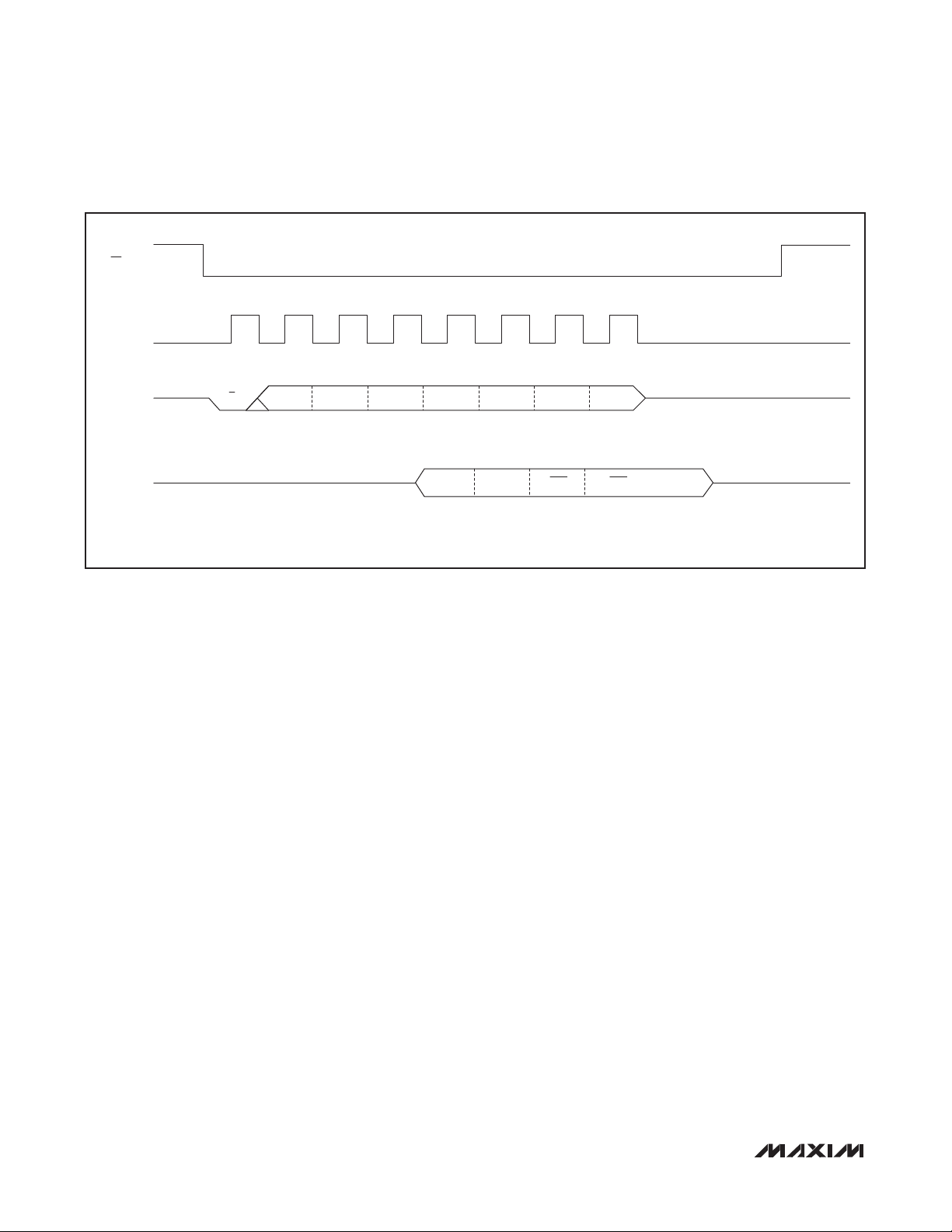
Dual Serial UART with 128-Word FIFOs
CS
SCLK
MAX3109
MOSI
MISO
Ax = REGISTER ADDRESS
Figure 20. SPI Fast Read Cycle
R
0
U
HIGH-Z
A4
A3 A2
00IRQ1 IRQ0
SPI Burst Access
Burst access allows writing and reading multiple data
bytes in one block by defining only the initial register
address in the SPI command byte. Multiple characters
can be loaded into the TxFIFO by using the THR (0x00)
as the initial burst write address. Similarly, multiple
characters can be read out of the RxFIFO by using the
RHR (0x00) as the SPI’s burst read address. If the SPI
burst address is different from 0x00, the MAX3109 automatically increments the register address after each SPI
data byte. Efficient programming of multiple consecutive
registers is thus possible. The chip-select input, CS/A0,
must be held low during the whole cycle. The SCLK/SCL
clock continues clocking throughout the burst access
cycle. The burst cycle ends when the SPI master pulls
CS/A0 high.
For example, writing 128 bytes into the TxFIFO can be
achieved by a burst write access using the following
sequence:
1) Pull CS/A0 low.
2) Send SPI write command to address 0x00.
3) Send 128 bytes.
4) Release CS/A0.
This takes a total of (1 + 128) x 8 clock cycles.
A1
A0
Fast Read Cycle
The two UART interrupts on the MAX3109 share the
single IRQ output. When operating in interrupt-based
mode, the microcontroller needs to locate the source
of the interrupt (i.e., which of the UARTs generated the
interrupt) and clear the interrupt.
In order to locate the source of an interrupt more quickly,
the MAX3109 implements the SPI fast read cycle. This
means that the microcontroller can determine which
UART is the source of the interrupt (UART0 or UART1)
using only 8 clock cycles (Figure 20). The U bit is
ignored during the fast read cycle.
I2C Interface
The MAX3109 contains an I2C-compatible interface for
data communication with a host processor (SCL and
SDA). The interface supports a clock frequency of up
to 1MHz. SCL and SDA require pullup resistors that are
connected to a positive supply.
START, STOP, and Repeated START Conditions
When writing to the MAX3109 using I2C, the master
sends a START condition (S) followed by the MAX3109
I2C address. After the address, the master sends
the register address of the register that is to be programmed. The master then ends communication by
issuing a STOP condition (P) to relinquish control of the
58 _____________________________________________________________________________________
Page 59

Dual Serial UART with 128-Word FIFOs
rP
bus, or a repeated START condition (Sr) to communicate to another I2C slave. See Figure 21.
Slave Address
The MAX3109 includes a configurable 7-bit I2C slave
address, allowing up to 16 MAX3109 devices to share
the same I2C bus. The address is defined by connecting the MOSI/A1 and CS/A0 inputs to DGND, VL, SCL,
or SDA (Table 5). Set the R/W bit high to configure the
MAX3109 to read mode. Set the R/W bit low to configure the MAX3109 to write mode. The address is the
Table 8. I2C Address Map
MOSI/A1
DGND DGND 0xD8 0xD9 0xB8 0xB9
DGND V
DGND SCL 0xC4 0xC5 0xA4 0xA5
DGND SDA 0xC6 0xC7 0xA6 0xA7
V
L
V
L
V
L
V
L
SCL DGND 0xD0 0xD1 0xB0 0xB1
SCL V
SCL SCL 0xD4 0xD5 0xB4 0xB5
SCL SDA 0xD6 0xD7 0xB6 0xB7
SDA DGND 0xC0 0xC1 0xA0 0xA1
SDA V
SDA SCL 0xDC 0xDD 0xBC 0xBD
SDA SDA 0xDE 0xDF 0xBE 0xBF
CS/A0
L
DGND 0xC8 0xC9 0xA8 0xA9
V
L
SCL 0xCC 0xCD 0xAC 0xAD
SDA 0xCE 0xCF 0xAE 0xAF
L
L
WRITE READ WRITE READ
0xC2 0xC3 0xA2 0xA3
0xCA 0xCB 0xAA 0xAB
0xD2 0xD3 0xB2 0xB3
0xDA 0xDB 0xBA 0xBB
first byte of information sent to the MAX3109 after the
MAX3109
START condition.
Bit Transfer
One data bit is transferred on the rising edge of each
SCL clock cycle. The data on SDA must remain stable
during the high period of the SCL clock pulse. Changes
in SDA while SCL is high and stable are considered
control signals (see the START, STOP, and Repeated
START Conditions section). Both SDA and SCL remain
high when the bus is not active.
UART0 UART1
SS
SCL
SDA
Figure 21. I2C START, STOP, and Repeated START Conditions
______________________________________________________________________________________ 59
Page 60

Dual Serial UART with 128-Word FIFOs
WRITE SINGLE BYTE
MAX3109
Figure 22. Write Byte Sequence
Figure 23. Burst Write Sequence
S
BURST WRITE
S DEVICE SLAVE ADDRESS - W A
FROM MASTER TO STAVE FROM SLAVE TO MASTER
DEVICE SLAVE ADDRESS - W A
8 DATA BITS
FROM MASTER TO STAVE
8 DATA BITS - 1
FROM SLAVE TO MASTER
A
REGISTER ADDRESS A
A
P
REGISTER ADDRESS A
8 DATA BITS - 2 A
8 DATA BITS - N A
P
Single-Byte Write
In this operation, the master sends an address and two
data bytes to the slave device (Figure 22). The following
procedure describes the single-byte write operation:
1) The master sends a START condition.
2) The master sends the 7-bit slave address plus a write
bit (low).
3) The addressed slave asserts an ACK on the data line.
4) The master sends the 8-bit register address.
5) The slave asserts an ACK on the data line only if the
address is valid (NACK if not).
6) The master sends 8 data bits.
7) The slave asserts an ACK on the data line.
8) The master generates a STOP condition.
In this operation, the master sends an address and multiple data bytes to the slave device (Figure 23). The slave
device automatically increments the register address
after each data byte is sent, unless the register being
accessed is 0x00, in which case the register address
remains the same. The following procedure describes
the burst write operation:
1) The master sends a START condition.
2) The master sends the 7-bit slave address plus a write
bit (low).
3) The addressed slave asserts an ACK on the data line.
4) The master sends the 8-bit register address.
5) The slave asserts an ACK on the data line only if the
address is valid (NACK if not).
6) The master sends 8 data bits.
7) The slave asserts an ACK on the data line.
8) Repeat 6 and 7 N-1 times.
9) The master generates a STOP condition.
60 _____________________________________________________________________________________
Burst Write
Page 61

Dual Serial UART with 128-Word FIFOs
2A
Single-Byte Read
In this operation, the master sends an address plus two
data bytes and receives one data byte from the slave
device (Figure 24). The following procedure describes
the single-byte read operation:
1) The master sends a START condition.
2) The master sends the 7-bit slave address plus a write
bit (low).
3) The addressed slave asserts an ACK on the data line.
4) The master sends the 8-bit register address.
5) The active slave asserts an ACK on the data line only
if the address is valid (NACK if not).
6) The master sends a repeated START condition.
7) The master sends the 7-bit slave address plus a read
bit (high).
8) The addressed slave asserts an ACK on the data line.
9) The slave sends 8 data bits.
READ SINGLE BYTE
S
DEVICE SLAVE ADDRESS - W A
10) The master asserts a NACK on the data line.
MAX3109
11) The master generates a STOP condition.
Burst Read
In this operation, the master sends an address plus
two data bytes and receives multiple data bytes from
the slave device (Figure 25). The following procedure
describes the burst byte read operation:
1) The master sends a START condition.
2) The master sends the 7-bit slave address plus a write
bit (low).
3) The addressed slave asserts an ACK on the data line.
4) The master sends the 8-bit register address.
5) The slave asserts an ACK on the data line only if the
address is valid (NACK if not).
6) The master sends a repeated START condition.
7) The master sends the 7-bit slave address plus a read
bit (high).
REGISTER ADDRESS A
Figure 24. Read Byte Sequence
BURST READ
Figure 25. Burst Read Sequence
Sr
S
Sr
FROM MASTER TO STAVE FROM SLAVE TO MASTER
DEVICE SLAVE ADDRESS - R
FROM MASTER TO STAVE FROM SLAVE TO MASTER
DEVICE SLAVE ADDRESS - W A
DEVICE SLAVE ADDRESS - R
A
A
A 8 DATA BITS - 38 DATA BITS -
8 DATA BITS NA
REGISTER ADDRESS A
8 DATA BITS - 1A
8 DATA BITS - NNA
P
P
______________________________________________________________________________________ 61
Page 62
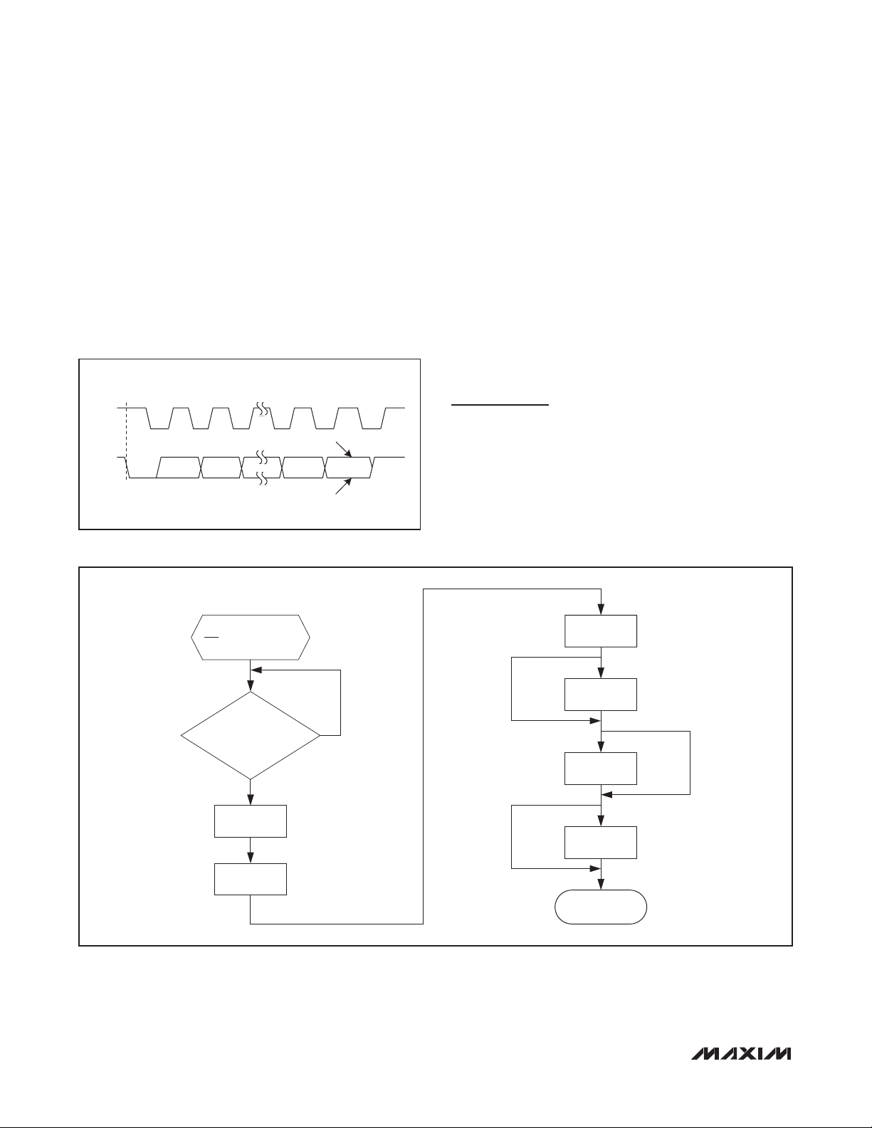
Dual Serial UART with 128-Word FIFOs
8) The slave asserts an ACK on the data line.
9) The slave sends 8 data bits.
10) The master asserts an ACK on the data line.
11) Repeat 9 and 10 N-2 times.
12) The slave sends the last 8 data bits.
13) The master asserts a NACK on the data line.
MAX3109
14) The master generates a STOP condition.
S
SCL
SDA
Figure 26. Acknowledge
12 89
NOT-ACKNOWLEDGE
ACKNOWLEDGE
Acknowledge Bits
Data transfers are acknowledged with an acknowledge
bit (ACK) or a not-acknowledge bit (NACK). Both the
master and the MAX3109 generate ACK bits. To generate
an ACK, pull SDA low before the rising edge of the ninth
clock pulse and hold it low during the high period of the
ninth clock pulse (Figure 26). To generate a NACK, leave
SDA high before the rising edge of the ninth clock pulse
and leave it high for the duration of the ninth clock pulse.
Monitoring for NACK bits allows for detection of unsuccessful data transfers.
Applications Information
Startup and Initialization
The MAX3109 can be initialized following power-up,
a hardware reset, or a software reset as shown in
Figure 27. To verify that the MAX3109 is ready for operation after a power-up or reset.
Repeatedly read a known register until the expected
contents are returned. The MAX3109 is ready for operation after approximately 200Fs.
POWER-UP/
RST INPUT PULLED HIGH
IS
DIVLSB READ
SUCCESSFULLY?
Y
CONFIGURE
CLOCKING
CONFIGURE
MODES
Figure 27. Startup and Initialization Flowchart
ENABLE
INTERRUPTS
CONFIGURE
FIFO CONTROL
N
CONFIGURE
FLOW CONTROL
CONFIGURE
GPIOs
START
COMMUNICATION
62 _____________________________________________________________________________________
Page 63
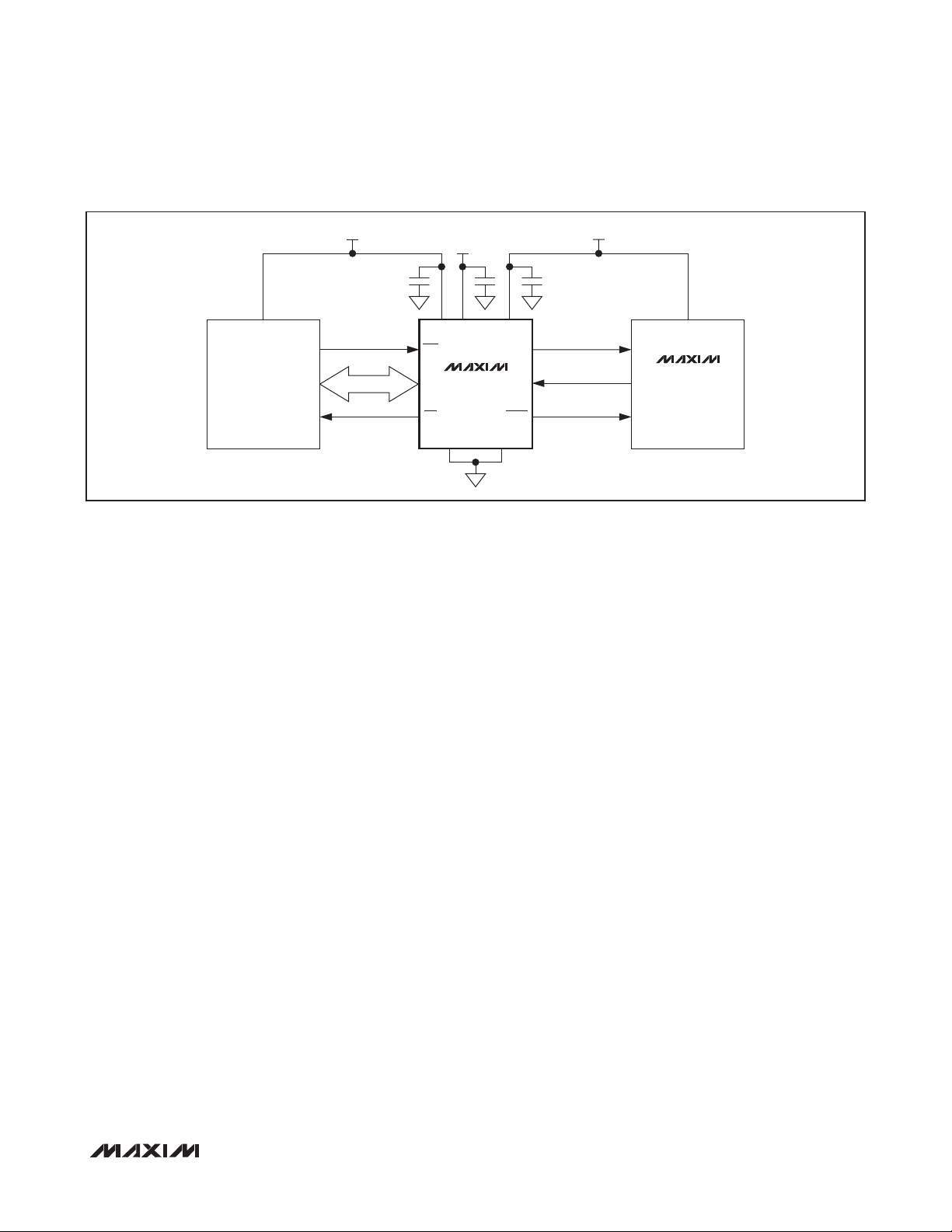
Dual Serial UART with 128-Word FIFOs
1.8V 3.3V
2.5V
MAX3109
RST
IRQ
V
LVCC
AGND
V
DD
MICROCONTROLLER
Figure 28. Logic-Level Translation
SPI/I
2
C
Low-Power Operation
To reduce the power consumption during normal operation, the following techniques can be adopted:
• Do not use the internal PLL. This saves the most
power of the options listed here. Disable and bypass
the PLL. With the PLL enabled, the current to the
VCC supply is in the range of a few mA (depending
on clock frequency and multiplication factor), while it
drops to below 1mA if disabled.
• Use an external clock source. The lowest power
clocking mode is when an external clock signal is
used. This drops the power consumption to about half
that of an external crystal.
• Keeptheinternalclockratesaslowaspossible.
• UsealowvoltageontheVCC supply.
• Use an external 1.8V supply. This saves the power
dissipated by the internal 1.8V linear regulator for the
1.8V core supply. Connect an external 1.8V supply to
V18 and disable the internal regulator by connecting
LDOEN to DGND.
MAX3109
DGND
V
EXT
TX_
RX_
RTS_
DI
RO
DE
V
CC
MAX14840E
TRANSCEIVER
Interrupts and Polling
Monitor the MAX3109 by polling the ISR register or by
monitoring the IRQ output. In polled mode, the IRQ
physical interrupt output is not used and the host controller polls the ISR register at frequent intervals to establish
the state of the MAX3109.
Alternatively, the physical IRQ interrupt can be used to
interrupt the host controller after specified events, making polling unnecessary. The IRQ output is an open-drain
output that requires a pullup resistor to VL.
Logic-Level Translation
The MAX3109 can be directly connected to transceivers
and controllers that have different supply voltages. The VL
input defines the logic voltage levels of the controller interface, while the V
voltage defines the logic of the trans-
EXT
ceiver interface. This ensures flexibility when selecting a
controller and transceiver. Figure 28 shows an example
of a configuration where the controller, transceiver, and
the MAX3109 are powered by three different supplies.
______________________________________________________________________________________ 63
Page 64

Dual Serial UART with 128-Word FIFOs
Power-Supply Sequencing
The device’s power supplies can be turned on in any
order. Each supply can be present over the entire specified range regardless of the presence or level of the
others. Ensure the presence of the interface supplies VL
and V
before sending input signals to the controller
EXT
and transceiver interfaces.
MAX3109
TX_
MAX3109
OE
MAX13481E
RX_
D+
D-
Figure 29. Connector Sharing with a USB Transceiver
SHARED
CONNECTOR
TX/D+
RX/D-
Connector Sharing
The TX_ and RTS_ outputs can be programmed to be
high impedance. This feature is used in cases where the
MAX3109 shares a common connector with other communications devices. Set the output of the MAX3109 to
high impedance when the other communication devices
are active. Set the MODE1[2]: TxHiZ bit high to set TX_
to a high-impedance state. Set the MODE1[3]: RTSHiZ
bit high to set RTS_ to a high-impedance state. Figure 29
shows an example of connector sharing with a USB
transceiver.
RS-232 5x3 Application
The four GPIOs can be used to implement the other flow
control signals defined in ITU V.24. Figure 30 shows how
the GPIOs create the DSR, DTR, DCD, and RI signals
found on some RS-232/V.28 interfaces.
Set the FlowCtrl[1:0] bits high to enable automatic hardware RTS_/CTS_ flow control.
MICROCONTROLLER
Figure 30. RS-232 Application
SPI/I2C
RST
IRQ
LDOEN
MAX3109
TX0
RX0
RTS0
CTS0
GPIO0
GPIO1
GPIO2
GPIO3
T1IN
R1OUT
T2IN
R2OUT
T3IN
R3OUT
R4OUT
R5OUT
MAX3245
Tx
Rx
RTS
CTS
DTR
DSR
DCD
RI
64 _____________________________________________________________________________________
Page 65
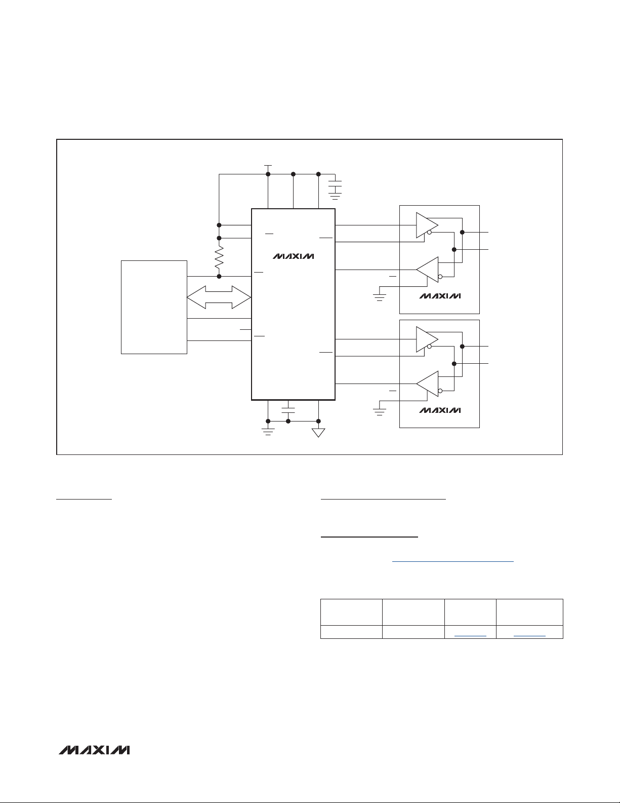
Dual Serial UART with 128-Word FIFOs
3.3V
0.1
µF
V
MICROCONTROLLER
10kΩ
SPI
CCVEXTVL
LDOEN
SPI/I2C
MAX3109
IRQ
XIN
XOUT
RST
AGND DGNDV
TX0
RTS0
RX0
TX1
RTS1
RX1
18
0.1µF
DI
DE
RO
RE
MAX14840E
DI
DE
RO
RE
MAX14840E
A1
B1
A2
B2
MAX3109
Figure 31. RS-485 Half-Duplex Application
Typical Application Circuit
Figure 31 shows the MAX3109 being used in a halfduplex RS-485 application. The microcontroller, the
RS-485 transceiver, and the MAX3109 are powered by a
single 3.3V supply. SPI is used as the controller’s communication interface. The microcontroller provides an
external clock source to clock the UART.
The MAX14840 receiver is always enabled, so echoing
occurs. Enable auto echo suppression in the MAX3109
by setting the MODE2[7]: EchoSuprs bit high.
Set the MODE1[4]: TranscvCtrl bit high to enable auto
transceiver direction control in order to automatically
control the DE input of the transceiver.
______________________________________________________________________________________ 65
Chip Information
PROCESS: BiCMOS
Package Information
For the latest package outline information and land patterns
(footprints), go to www.maxim-ic.com/packages. Note that a
“+”, “#”, or “-” in the package code indicates RoHS status only.
Package drawings may show a different suffix character, but
the drawing pertains to the package regardless of RoHS status.
PACKAGE
TYPE
32 TQFN-EP T3255+1
PACKAGE
CODE
OUTLINE
NO.
LAND
PATTERN NO.
21-0180 90-0012
Page 66

Dual Serial UART with 128-Word FIFOs
Revision History
REVISION
NUMBER
0 3/11 Initial release —
1 5/12
REVISION
DATE
MAX3109
DESCRIPTION
Corrected for improved shutdown current mode and specifications, including lowpower shutdown mode configurations
PAGES
CHANGED
1, 7, 14, 15,
27, 38, 62
Maxim cannot assume responsibility for use of any circuitry other than circuitry entirely embodied in a Maxim product. No circuit patent licenses are implied.
Maxim reserves the right to change the circuitry and specifications without notice at any time.
66 Maxim Integrated Products, 120 San Gabriel Drive, Sunnyvale, CA 94086 408-737-7600
©
2012 Maxim Integrated Products Maxim is a registered trademark of Maxim Integrated Products, Inc.
 Loading...