

Page 1
General Description
The MAX3100 universal asynchronous receiver transmitter (UART) is the first UART specifically optimized for
small microcontroller-based systems. Using an
SPI™/MICROWIRE™ interface for communication with
the host microcontroller (µC), the MAX3100 comes in a
compact 16-pin QSOP. The asynchronous I/O is suitable
for use in RS-232, RS-485, IR, and opto-isolated data
links. IR-link communication is easy with the MAX3100’s
infrared data association (IrDA) timing mode.
The MAX3100 includes a crystal oscillator and a baudrate generator with software-programmable divider ratios
for all common baud rates from 300 baud to 230k baud.
A software- or hardware-invoked shutdown lowers quiescent current to 10µA, while allowing the MAX3100 to
detect receiver activity.
An 8-word-deep first-in/first-out (FIFO) buffer minimizes
processor overhead. This device also includes a flexible
interrupt with four maskable sources, including address
recognition on 9-bit networks. Two hardware-handshaking control lines are included (one input and one output).
The MAX3100 is available in 14-pin plastic DIP and small,
16-pin QSOP packages in the commercial and extended
temperature ranges.
________________________Applications
Handheld Instruments
Intelligent Instrumentation
UART in SPI Systems
Small Networks in HVAC or Building Control
Isolated RS-232/RS-485: Directly Drives Opto-Couplers
Low-Cost IR Data Links for Computers/Peripherals
____________________________Features
♦ Small TQFN and QSOP Packages Available
♦ Full-Featured UART:
—IrDA SIR Timing Compatible
—8-Word FIFO Minimizes Processor
Overhead at High Data Rates
—Up to 230k Baud with a 3.6864MHz Crystal
—9-Bit Address-Recognition Interrupt
—Receive Activity Interrupt in Shutdown
♦ SPI/MICROWIRE-Compatible µC Interface
♦ Lowest Power:
—150µA Operating Current at 3.3V
—10µA in Shutdown with Receive Interrupt
♦ +2.7V to +5.5V Supply Voltage in Operating Mode
♦ Schmitt-Trigger Inputs for Opto-Couplers
♦ TX and RTS Outputs Sink 25mA for Opto-Couplers
MAX3100
SPI/MICROWIRE-Compatible
UART in QSOP-16
________________________________________________________________
Maxim Integrated Products
1
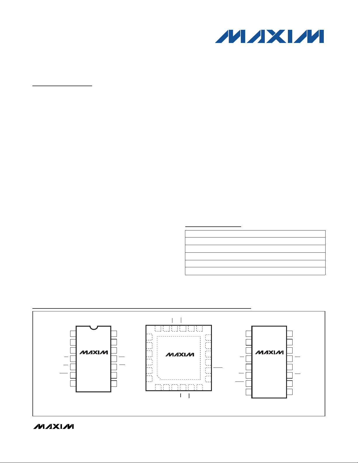
Pin Configurations
19-1259; Rev 2; 1/09
PART
MAX3100CPD+
MAX3100CEE+ 0°C to +70°C
0°C to +70°C
TEMP RANGE PIN-PACKAGE
14 Plastic DIP
16 QSOP
Ordering Information
Typical Operating Circuit appears at end of data sheet.
SPI is a trademark of Motorola, Inc. MICROWIRE is a trademark of National Semiconductor Corp.
MAX3100EPD+
MAX3100EEE+ -40°C to +85°C
-40°C to +85°C 14 Plastic DIP
16 QSOP
MAX3100ETG+ -40°C to +85°C 24 TQFN-EP*
For pricing, delivery, and ordering information, please contact Maxim Direct at 1-888-629-4642,
or visit Maxim’s website at www.maxim-ic.com.
+
Denotes a lead(Pb)-free/RoHS-compliant package.
EP = Exposed pad.
TOP VIEW
DIN
DOUT
SCLK
IRQ
SHDN
GND
+ +
1
2
3
MAX3100
4
5
6
7
DIP
V
14
CC
13
TX
12
RX
11
RTSCS
CTS
10
X1
9
X2
8
N.C.
N.C.
TX
V
CC
DIN
N.C.
*EP = EXPOSED PAD, CONNECT EP TO GROUND
N.C.
18 17 16 15 14 13
19
20
21
22
23
24
+
123456
N.C.
CTS
RTS
RX
MAX3100
DOUT
TQFN-EP
SCLK
N.C.
N.C.
DIN
12
N.C.
11
X1
10
X2
GND
9
SHDN
8
*EP
CS
IRQ
N.C.
N.C.
7
DOUT
SCLK
N.C.
IRQ
SHDN
GND
1
2
3
CS
MAX3100
4
5
6
7
8
QSOP
16
15
14
13
12
11
10
9
V
TX
RX
RTS
N.C.
CTS
X1
X2
CC
Page 2

MAX3100
SPI/MICROWIRE-Compatible
UART in QSOP-16
2 _______________________________________________________________________________________
ABSOLUTE MAXIMUM RATINGS
ELECTRICAL CHARACTERISTICS
(VCC= +2.7V to +5.5V, TA= T
MIN
to T
MAX
, unless otherwise noted. Typical values are measured at 9600 baud at TA= +25°C.)
Stresses beyond those listed under “Absolute Maximum Ratings” may cause permanent damage to the device. These are stress ratings only, and functional
operation of the device at these or any other conditions beyond those indicated in the operational sections of the specifications is not implied. Exposure to
absolute maximum rating conditions for extended periods may affect device reliability.
VCCto GND ...........................................................................+6V
Input Voltage to GND
(CS, SHDN, X1, CTS, RX, DIN, SCLK) ....-0.3V to (V
CC
+ 0.3V)
Output Voltage to GND
(DOUT, RTS, TX, X2) ..............................-0.3V to (V
CC
+ 0.3V)
IRQ...........................................................................-0.3V to 6V
TX, RTS Output Current ....................................................100mA
X2, DOUT, IRQ Short-Circuit Duration
(to V
CC
or GND) .........................................................Indefinite
Continuous Power Dissipation (T
A
= +70°C)
Plastic DIP (derate 10.00mW/°C above +70°C) .......... 800mW
QSOP (derate 8.30mW/°C above +70°C).....................667mW
TQFN (derate 33.3mW/°C above +70°C) ................2666.7mW
Operating Temperature Ranges
MAX3100C_ _ ......................................................0°C to +70°C
MAX3100E_ _ ...................................................-40°C to +85°C
Storage Temperature Range ............................ -65°C to +160°C
Lead Temperature (soldering, 10s) ................................ +300°C
I
SOURCE
= 25µA, TX only
V
IRQ
= 5.5V
I
SINK
= 4mA
DOUT only, CS = V
CC
Shutdown mode
Active mode
I
SOURCE
= 5mA
V
VCC= 3.3V
VX1= 0V and 5.5V
CONDITIONS
VCC- 0.5
V
OH
Output High Voltage
pF5C
OUT
Output Capacitance
µA±1I
LK
Output Leakage
V0.4V
OL
Output Low Voltage
pF5C
OUT
Output Capacitance
µA±1I
LK
Output Leakage
DOUT, TX, RTS: I
SINK
= 4mA
TX, RTS: I
SINK
= 25mA
V
pF5C
IN
Input Capacitance
V0.3 x V
CC
V
IL
Input Low Voltage
V0.7 x V
CC
V
IH
Input High Voltage
0.4
V
OL
Output Low Voltage
0.9
VX1= 0V and 5.5V
VV
CC
/ 2 0.2 x V
CC
V
IL
Input Low Voltage
V0.7 x VCCV
CC
/ 2V
IH
Input High Voltage
V0.05 x V
CC
V
HYST
Input Hysteresis
µA±1I
IL
Input Leakage
pF5C
IN
Input Capacitance
UNITSMIN TYP MAXSYMBOLPARAMETER
2
I
IN
Input Current µA
25
VCC- 0.5
mA
0.27 1
I
CC
VCCSupply Current in
Normal Mode
SHDN bit = 1 or SHDN = 0,
logic inputs are at 0V or V
CC
µA10I
CC
VCCSupply Current in
Shutdown
With 1.8432MHz crystal;
all other logic inputs are at
0V or V
CC
VCC= 5V
VCC= 3.3V 0.15 0.4
V2.7 5.5V
CC
Supply Voltage
LOGIC INPUTS (DIN, SCLK, CS, SHDN, CTS, RX)
OSCILLATOR INPUT (X1)
OUTPUTS (DOUT, TX, RTS)
IRQ OUTPUT (Open Drain)
POWER REQUIREMENTS
Page 3
MAX3100
SPI/MICROWIRE-Compatible
UART in QSOP-16
_______________________________________________________________________________________ 3
ELECTRICAL CHARACTERISTICS (continued)
(VCC= +2.7V to +5.5V, TA= T
MIN
to T
MAX
, unless otherwise noted. Typical values are at TA= +25°C.)
C
LOAD
= 100pF
C
LOAD
= 100pF, RCS= 10kΩ
C
LOAD
= 100pF
CONDITIONS
ns100t
CL
SCLK Low Time
ns100t
CH
SCLK High Time
ns238t
CP
SCLK Period
ns0t
DH
DIN to SCLK Hold Time
ns100t
DS
DIN to SCLK Setup Time
ns100t
DO
SCLK Fall to DOUT Valid
ns0t
CSH
CS to SCLK Hold Time
ns100t
CSS
CS to SCLK Setup Time
ns100t
TR
CS High to DOUT Tri-State
ns100t
DV
CS Low to DOUT Valid
UNITSMIN TYP MAXSYMBOLPARAMETER
TX, RTS, DOUT: C
LOAD
= 100pF
(Note 1)
ns10t
r
Output Rise Time
ns200t
CSW
CS High Pulse Width
ns100t
CS0
SCLK Rising Edge
to CS Falling
(Note 1) ns200t
CS1
CS Rising Edge
to SCLK Rising
Figure 1. Detailed Serial-Interface Timing
TX, RTS, DOUT, IRQ: C
LOAD
= 100pF
ns10t
f
Output Fall Time
AC TIMING (Figure 1)
Note 1: t
CS0
and t
CS1
specify the minimum separation between SCLK rising edges used to write to other devices on the SPI bus
and the CS used to select the MAX3100. A separation greater than t
CS0
and t
CS1
ensures that the SCLK edge is ignored.
CS
t
CSS
t
DS
t
DH
t
DV
SCLK
DIN
DOUT
t
CSH
• • •
t
t
CL
CH
• • •
• • •
t
DO
• • •
t
CSH
t
TR
Page 4
MAX3100
SPI/MICROWIRE-Compatible
UART in QSOP-16
4 _______________________________________________________________________________________
__________________________________________Typical Operating Characteristics
(TA = +25°C, unless otherwise noted.)
SUPPLY CURRENT vs. TEMPERATURE
1000
900
800
700
600
500
400
300
SUPPLY CURRENT (μA)
200
100
0
-40 -20 40 60 100
020 80
TEMPERATURE (°C)
SUPPLY CURRENT vs. BAUD RATE
400
1.8432 MHz
CRYSTAL
350
300
250
200
SUPPLY CURRENT (μA)
150
100
50
3V
TRANSMITTING
1000
100 10k
1.8432MHz CRYSTAL
TRANSMITTING AT
115.2 kbps
VCC = 5V
VCC = 3.3V
5V
TRANSMITTING
BAUD RATE (bps)
5V
STANDBY
3V
STANDBY
100k 1M
10
9
MAX3100-01
8
7
6
5
4
3
SHUTDOWN CURRENT (μA)
2
1
0
-40 -20 40 60 100
TX, RTS, DOUT OUTPUT CURRENT
vs. OUTPUT LOW VOLTAGE (V
70
60
MAX3100-03a
50
40
30
20
OUTPUT SINK CURRENT (mA)
10
0
0 0.20.1 0.6 0.7
SHUTDOWN CURRENT
vs. TEMPERATURE
1.8432MHz CRYSTAL
VCC = 5V
020 80
TEMPERATURE (°C)
CC
RTS
TX
DOUT
0.3 0.50.4 0.9
VOLTAGE (V)
0.8
= 3.3V)
700
MAX3100-02
600
500
400
300
SUPPLY CURRENT (μA)
200
100
0
90
80
MAX3100-04
70
60
50
40
30
OUTPUT SINK CURRENT (mA)
20
10
1.0
0
SUPPLY CURRENT vs.
EXTERNAL CLOCK FREQUENCY
V
= 5V
CC
V
= 3.3V
CC
01 3
EXTERNAL CLOCK FREQUENCY (MHz)
2
TX, RTS, DOUT OUTPUT CURRENT
vs. OUTPUT LOW VOLTAGE (V
RTS
DOUT
0 0.20.1 0.6 0.7
0.3 0.50.4 0.9
VOLTAGE (V)
0.8
4
CC
MAX3100-03
5
= 5V)
MAX3100-05
TX
1.0
Page 5

MAX3100
SPI/MICROWIRE-Compatible
UART in QSOP-16
_______________________________________________________________________________________ 5
Detailed Description
The MAX3100 universal asynchronous receiver transmitter (UART) interfaces the SPI/MICROWIRE-compatible, synchronous serial data from a microprocessor
(µP) to asynchronous, serial-data communication ports
(RS-232, RS-485, IrDA). Figure 2 shows the MAX3100
functional diagram.
The MAX3100 combines a simple UART and a baudrate generator with an SPI interface and an interrupt
generator. Configure the UART by writing a 16-bit word
to a write-configuration register, which contains the
baud rate, data-word length, parity enable, and enable
of the 8-word receive first-in/first-out (FIFO). The write
configuration selects between normal UART timing and
IrDA timing, controls shutdown, and contains 4 interrupt
mask bits.
Transmit data by writing a 16-bit word to a write-data
register, where the last 7 or 8 bits are actual data to be
transmitted. Also included is the state of the transmitted
parity bit (if enabled). This register controls the state of
the RTS output pin. Received words generate an inter-
rupt if the receive-bit interrupt is enabled.
Read data from a 16-bit register that holds the oldest
data from the receive FIFO, the received parity data,
and the logic level at the CTS input pin. This register
also contains a bit that is the framing error in normal
operation and a receive-activity indicator in shutdown.
The baud-rate generator determines the rate at which
the transmitter and receiver operate. Bits B0 to B3 in
the write-configuration register determine the baud-rate
divisor (BRD), which divides down the X1 oscillator frequency. The baud clock is 16 times the data rate (baud
rate).
Pin Description
PIN
QSOP DIP
NAME FUNCTION
1 1 23 DIN SPI/MICROWIRE Serial-Data Input. Schmitt-trigger input.
2 2 2 DOUT SPI/MICROWIRE Serial-Data Output. High impedance when CS is high.
3 3 3 SCLK SPI/MICROWIRE Serial-Clock Input. Schmitt-trigger input.
444CS
Active-Low Chip-Select Input. DOUT goes high impedance when CS is high,
IRQ, TX, and RTS are always active. Schmitt-trigger input.
655IRQ Active-Low Interrupt Output. Open-drain interrupt output to microprocessor.
768SHDN
Hardware-Shutdown Input. When shut down (SHDN = 0), the oscillator turns
off immediately without waiting for the current transmission to end, reducing
supply current to just leakage currents.
8 7 9 GND Ground
9 8 10 X2
Crystal Connection. Leave X2 unconnected for external clock. See Crystal-
Oscillator Operation—X1, X2 Connection section.
10 9 11 X1
Crystal Connection. X1 also serves as an external clock input. See Crystal-
Oscillator Operation—X1, X2 Connection section.
11 10 15 CTS
General-Purpose Active-Low Input. Read via the CTS register bit; often used
for RS-232 clear-to-send input (Table 1).
13 11 16 RTS
General-Purpose Active-Low Output. Controlled by the CTS register bit. Often
used for RS-232 request-to-send output or RS-485 driver enable.
14 12 17 RX
Asynchronous Serial-Data (receiver) Input. The serial information received
from the modem or RS-232/RS-485 receiver. A transition on RX while in
shutdown generates an interrupt (Table 5).
15 13 21 TX Asynchronous Serial-Data (transmitter) Output
16 14 22 V
CC
Positive Supply Pin (2.7V to 5.5V)
5, 12 —
1, 6, 7, 12,
13, 14, 18,
N.C. No Connection. Not internally connected.
— — — EP Exposed Pad. Connect EP to ground or leave unconnected.
TQFN-EP
19, 20, 24
Page 6
MAX3100
SPI/MICROWIRE-Compatible
UART in QSOP-16
6 _______________________________________________________________________________________
Figure 2. Functional Diagram
The transmitter section accepts SPI/MICROWIRE data,
formats it, and transmits it in asynchronous serial format
from the TX output. Data is loaded into the transmit-
buffer register from the SPI/MICROWIRE interface. The
MAX3100 adds start and stop bits to the data and
clocks the data out at the selected baud rate (Table 7).
Pt TX-BUFFER REGISTER
9
9
(SOURCES)
PrRT
IRQ
INTERRUPT
LOGIC
RA/FE
DIN
CS
SCLK
DOUT
(MASKS)
TRANSMIT-DONE (TM)
DATA-RECEIVED (RM)
PARITY (PM)
FRAMING ERROR (RAM)/
RECEIVE ACTIVITY
SPI
INTERFACE
SHDN
TX-SHIFT REGISTER
Pt
B0
B1
B2
B3
RX-SHIFT REGISTER
PrPrRX-BUFFER REGISTER
Pr
D0t–D7t
X1
BAUD-RATE
BAUD-RATE
GENERATOR
GENERATOR
X2
D0r–D7r
9
RX-BUFFER REGISTER
9
XTAL
RA
FE
START/STOP-
ACTIVITY
DETECT
BIT DETECT
I / O
TX
RX
CTS
RTS
Page 7
MAX3100
The receiver section receives data in serial form. The
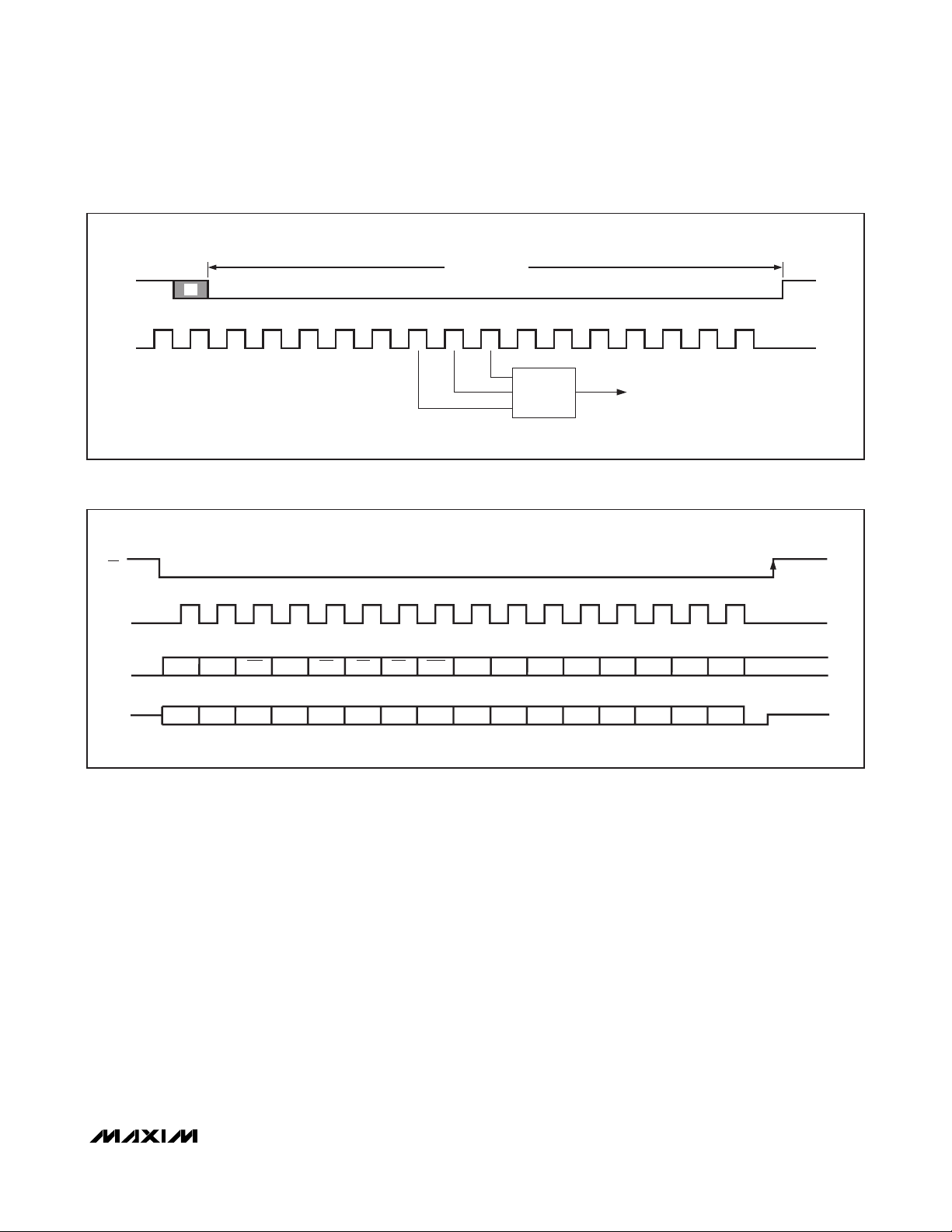
MAX3100 detects a start bit on a high-to-low RX transition (Figure 3). An internal clock samples data at 16
times the data rate. The start bit can occur as much as
one clock cycle before it is detected, as indicated by
the shaded portion. The state of the start bit is defined
as the majority of the 7th, 8th, and 9th sample of the
internal 16x baud clock. Subsequent bits are also
majority sampled. Receive data is stored in an 8-word
FIFO. The FIFO is cleared if it overflows.
The on-board oscillator can use a 1.8432MHz or
3.6864MHz crystal, or it can be driven at X1 with a 45%
to 55% duty-cycle square wave.
SPI Interface
The bit streams for DIN and DOUT consist of 16 bits,
with bits assigned as shown in the
MAX3100
Operations
section. DOUT transitions on SCLK’s falling
edge, and DIN is latched on SCLK’s rising edge (Figure
4). Most operations, such as the clearing of internal
registers, are executed only on CS’s rising edge. The
DIN stream is monitored for its first two bits to tell the
UART the type of data transfer being executed (Write
Config, Read Config, Write Data, Read Data).
Only 16-bit words are expected. If CS goes high in the
middle of a transmission (any time before the 16th bit),
the sequence is aborted (i.e., data does not get written
to individual registers). Every time CS goes low, a new
16-bit stream is expected. An example of a write configuration is shown in Figure 4.
SPI/MICROWIRE-Compatible
UART in QSOP-16
_______________________________________________________________________________________ 7
Figure 3. Start-Bit Timing
Figure 4. SPI Interface (Write Configuration)
ONE BAUD PERIOD
RX
A
BAUD
BLOCK
CS
SCLK
DIN
DOUT
1
1
11 FEN SHDN TM RM PM RAM IR ST PE L B3 B2 B1 B0
RT 00 000 00 00 00 000
23456 789
2 3 4 5 6 7 8 9 10 11 12 13 14 15 16
10 11
MAJORITY
CENTER
SAMPLER
12 13 14 15 16
DATA
UPDATED
Page 8

MAX3100
SPI/MICROWIRE-Compatible
UART in QSOP-16
8 _______________________________________________________________________________________
MAX3100 Operations
Write Operations
Table 1 shows write-configuration data. A 16-bit
SPI/MICROWIRE write configuration clears the receive
FIFO and the R, T, RA/FE, D0r–D7r, D0t–D7t, Pr, and Pt
registers. RTS and CTS remain unchanged. The new
configuration is valid on CS’s rising edge if the transmit
buffer is empty (T = 1) and transmission is over. If the
latest transmission has not been completed, the registers are updated when the transmission is over (T = 0).
The write-configuration bits (FEN, SHDNi, IR, ST, PE, L,
B3–B0) take effect after the current transmission is
over. The mask bits (TM, RM, PM, RAM) take effect
immediately after the 16th clock’s rising edge at SCLK.
Read Operations
Table 2 shows read-configuration data. This register
reads back the last configuration written to the
MAX3100. The device enters test mode if bit 0 = 1. In
this mode, if CS = 0, the RTS pin acts as the 16x clock
generator’s output. This may be useful for direct baudrate generation (in this mode, TX and RX are in digital
loopback).
Normally, the write-data register loads the TX-buffer
register. To change the RTS pin’s state without writing
data, set the TE bit. Setting the TE bit high inhibits the
write command (Table 3).
Reading data clears the R bit and interrupt IRQ (Table 4).
Register Functions
Table 5 shows read/write operation and power-on reset
state (POR), and describes each bit used in programming the MAX3100. Figure 5 shows parity and wordlength control.
14
0
T
6
D6t
D6r
7
D7t
D7r
15 2
DIN 1 D2t
DOUT R D2r
BIT 3
D3t
D3r
0
D0t
D0r
1
D1t
D1r
4
D4t
D4r
5
D5t
D5r
10
TE
RA/FE
11
0
0
8
Pt
Pr
9
RTS
CTS
12
0
0
13
0
0
14
0
T
6
0
D6r
7
0
D7r
15 2
DIN 0 0
DOUT R D2r
BIT 3
0
D3r
0
0
D0r
1
0
D1r
4
0
D4r
5
0
D5r
10
0
RA/FE
11
0
0
8
0
Pr
9
0
CTS
12
0
0
13
0
0
Table 3. Write Data (D15, D14 = 1, 0)
Table 4. Read Data (D15, D14 = 0, 0)
14
1
T
6
0
ST
7
0
IR
15 2
DIN 0 0
DOUT R B2
BIT 3
0
B3
0
TEST
B0
1
0
B1
4
0
L
5
0
PE
10
0
RM
11
0
TM
8
0
RAM
9
0
PM
12
0
SHDNo
13
0
FEN
Table 2. Read Configuration (D15, D14 = 0, 1)
6
ST
0
7
IR
0
2
B2
0
3
B3
0
0
B0
0
1
B1
0
4
L
0
5
PE
0
10
RM
0
11
TM
0
8
RAM
0
9
PM
0
12
SHDNi
0
13
FEN
0
15 14
1
T
DIN 1
DOUT R
BIT
Table 1. Write Configuration (D15, D14 = 1, 1)
Page 9

MAX3100
SPI/MICROWIRE-Compatible
UART in QSOP-16
_______________________________________________________________________________________ 9
POR
STATE
DESCRIPTION
0000
0000
XPr r
Receive-Parity Bit. This bit is the extra bit received if PE = 1. Therefore, PE = 1 results in 9-bit
transmissions (L = 0). If PE = 0, then Pr is set to 0. Pr is stored in the FIFO with the receive
data (see the
Nine-Bit Networks
section).
0
0
IR r Reads the value of the IR bit.
L
READ/
WRITE
w
B0–B3 w Baud-Rate Divisor Select Bits. Sets the baud clock’s value (Table 6).
B0–B3 r Baud-Rate Divisor Select Bits. Reads the 4-bit baud clock value assigned to these registers.
BIT
NAME
Bit for setting the word length of the transmitted or received data. L = 0 results in 8-bit words
(9-bit words if PE = 1), see Figure 5. L = 1 results in 7-bit words (8-bit words if PE = 1).
0
X
L r Reads the value of the L bit.
Pt w
Transmit-Parity Bit. This bit is treated as an extra bit that will be transmitted if PE = 1. To be
useful in 9-bit networks, the MAX3100 does not calculate parity. If PE = 0, then this bit (Pt) is
ignored in transmit mode (see the
Nine-Bit Networks
section).
00000000
0
D0r–D7r r
Eight data bits read from the receive FIFO or the receive register. These will be all 0s when
the receive FIFO or the receive registers are empty. When L = 1, D7r is always 0.
FEN
w
FIFO Enable. Enables the receive FIFO when FEN = 0. When FEN = 1, FIFO is disabled.
0
0
FEN
r
FIFO-Enable Readback. FEN’s state is read.
IR w Enables the IrDA timing mode when IR = 1.
No
change
X
CTS r
Clear-to-Send-Input. Records the state of the CTS pin (CTS bit = 0 implies CTS pin = logic
high).
D0t–D7t w
Transmit-Buffer Register. Eight data bits written into the transmit-buffer register. D7t is ignored
when L = 1.
Table 5. Bit Descriptions
0PE w
Parity-Enable Bit. Appends the Pt bit to the transmitted data when PE = 1, and sends the Pt
bit as written. No parity bit is transmitted when PE = 0. With PE = 1, an extra bit is expected to
be received. This data is put into the Pr register. Pr = 0 when PE = 0. The MAX3100 does not
calculate parity.
0PE r Reads the value of the Parity-Enable bit.
0
PM
w
Mask for Pr bit. IRQ is asserted if PM = 1 and Pr = 1 (Table 6).
0
PM
r
Reads the value of the PM bit (Table 6).
0R r
Receive Bit or FIFO Not Empty Flag. R = 1 means new data is available to be read from the
receive register or FIFO.
0
RM
w
Mask for R bit. IRQ is asserted if RM = 1 and R = 1 (Table 6).
0
RM
r
Reads the value of the RM bit (Table 6).
0
RAM
w
Mask for RA/FE bit. IRQ is asserted if RAM = 1 and RA/FE = 1 (Table 6).
0
RAM
r
Reads the value of the RAM bit (Table 6).
0RTS w
Request-to-Send Bit. Controls the state of the RTS output. This bit is reset on power-up (RTS
bit = 0 sets the RTS pin = logic high).
Page 10

Table 5. Bit Descriptions (continued)
MAX3100
SPI/MICROWIRE-Compatible
UART in QSOP-16
10 ______________________________________________________________________________________
POR
STATE
DESCRIPTION
READ/
WRITE
BIT
NAME
0SHDNi w
Software-Shutdown Bit. Enter software shutdown with a write configuration where SHDNi = 1.
Software shutdown takes effect after CS goes high, and causes the oscillator to stop as soon
as the transmitter becomes idle. Software shutdown also clears R, T, RA/FE, D0r–D7r,
D0t–D7t, Pr, Pt, and all data in the receive FIFO. RTS and CTS can be read and updated
while in shutdown. Exit software shutdown with a write configuration where SHDNi = 0. The
oscillator restarts typically within 50ms of CS going high. RTS and CTS are unaffected. Refer
to the
Pin Description
for hardware shutdown (SHDN input).
0SHDNo r
Shutdown Read-Back Bit. The read-configuration register outputs SHDNo = 1 when the UART
is in shutdown. Note that this bit is not sent until the current byte in the transmitter is sent (T =
1). This tells the processor when it may shut down the RS-232 driver. This bit is also set immediately when the device is shut down through the SHDN pin.
0RA/FE r
Receiver-Activity/Framing-Error Bit. In shutdown mode, this is the RA bit. In normal operation,
this is the FE bit. In shutdown mode, a transition on RX sets RA = 1. In normal mode, a framing error sets FE = 1. A framing error occurs if a zero is received when the first stop bit is
expected. FE is set when a framing error occurs, and cleared upon receipt of the next properly framed character independent of the FIFO being enabled. When the device wakes up, it is
likely that a framing error will occur. This error can be cleared with a write configuration. The
FE bit is not cleared on a Read Data operation. When an FE is encountered, the UART resets
itself to the state where it is looking for a start bit.
0ST w
Transmit-Stop Bit. One stop bit will be transmitted when ST = 0. Two stop bits will be transmitted when ST = 1. The receiver only requires one stop bit.
0ST r Reads the value of the ST bit.
0
TM
w
Mask for T bit. IRQ is asserted if TM = 1 and T = 1 (Table 6).
0
TM
r
Reads the value of the TM bit (Table 6).
1T r
Transmit-Buffer-Empty Flag. T = 1 means that the transmit buffer is empty and ready to
accept another data word.
0
TE
w
Transmit-Enable Bit. If TE = 1, then only the RTS pin will be updated on CS’s rising edge. The
contents of RTS, Pt, and D0t–D7t transmit on CS’s rising edge when TE = 0.
Figure 5. Parity and Word-Length Control
PE = 0, L = 0
IDLE
IDLE
IDLE
IDLE
TIME
D0START D1 D2 D3 D4 D5 D6 D7 STOP STOP IDLE
PE = 0, L = 1
D0START D1 D2 D3 D4 D5 D6 STOP STOP IDLE
PE = 1, L = 0
D0START D1 D2 D3 D4 D5 D6 D7 Pt STOP STOP IDLE
PE = 1, L = 1
D0START D1 D2 D3 D4 D5 D6 Pt
SECOND STOP BIT IS OMITTED IF ST = 0.
STOPSTOP
IDLE
Page 11

MAX3100
SPI/MICROWIRE-Compatible
UART in QSOP-16
______________________________________________________________________________________ 11
Figure 6. Interrupt Sources and Masks Functional Diagram
Table 6. Interrupt Sources and Masks—Bit Descriptions
MEANING
WHEN SET
DESCRIPTION
Received parity bit = 1
Transition on RX when
in shutdown; framing
error when not in
shutdown
RA/FE
RAM
This is the RA (RX-transition) bit in shutdown, and the FE (framing-error) bit in
operating mode. RA is set if there has been a transition on RX since entering
shutdown. RA is cleared when the MAX3100 exits shutdown. IRQ is asserted
when RA is set and RAM = 1.
FE is determined solely by the currently received data, and is not stored in FIFO.
The FE bit is set if a zero is received when the first stop bit is expected. FE is
cleared upon receipt of the next properly framed character. IRQ is asserted
when FE is set and RAM = 1.
MASK
BIT
Pr
PM
The Pr bit reflects the value in the word currently in the receive-buffer register
(oldest data available). The Pr bit is set when parity is enabled (PE = 1) and the
received parity bit is 1. The Pr bit is cleared either when parity is not enabled (PE
= 0), or when parity is enabled and the received bit is 0. An interrupt is issued
based on the oldest Pr value in the receiver FIFO. The oldest Pr value is the next
value that will be read by a Read Data operation.
BIT
NAME
Data availableR
RM
The R bit is set when new data is available to be read from the receive register/
FIFO. FIFO is cleared when all data has been read. An interrupt is asserted as long
as R = 1 and RM = 1.
Transmit buffer is
empty
T
TM
The T bit is set when the transmit buffer is ready to accept data. IRQ is asserted
low if TM = 1 and the transmit buffer becomes empty. This source is cleared on
CS’s rising edge during a Read Data operation. Although the interrupt is cleared,
T may be polled to determine transmit-buffer status.
Interrupt Sources and Masks
A Read Data operation clears the interrupt IRQ. Table
6 gives the details for each interrupt source. Figure 6
shows the functional diagram for the interrupt sources
and mask blocks.
IRQ
N
R
T
Pr
RA
FE
Q
RM MASK
Q
TM MASK
Q
PM MASK
TRANSITION ON RX
RAM MASK
FRAMING ERROR
RAM MASK
DATA READ
R
S
TRANSMIT BUFFER EMPTY
R
DATA READ
S
PE = 1 AND RECEIVED PARITY BIT = 1
R
PE = 0 OR RECEIVED PARITY BIT = 0
SHUTDOWN
SHUTDOWN
NEW DATA AVAILABLE
S
Page 12

Clock-Oscillator Baud Rates
Bits B0–B3 of the write-configuration register determine
the baud rate. Table 7 shows baud-rate divisors for given
input codes, as well as the given baud rate for
1.8432MHz and 3.6864MHz crystals. Note that the baud
rate = crystal frequency / 16x division ratio.
Shutdown Mode
In shutdown, the oscillator turns off to reduce power
dissipation (ICC< 10µA). The MAX3100 enters shutdown in one of two ways: by a software command
(SHDNi bit = 1) or by a hardware command (SHDN =
logic low). The hardware shutdown is effective immediately and will immediately terminate any transmission in
progress. The software shutdown, requested by setting
SHDNi bit = 1, is entered upon completing the transmission of the data in both the transmit register and the
transmit-buffer register. The SHDNo bit is set when the
MAX3100 enters shutdown (either hardware or software). The microcontroller (µC) can monitor the SHDNo
bit to determine when all data has been transmitted,
and shut down any external circuitry (such as RS-232
transceivers) at that time.
Shutdown clears the receive FIFO, R, A, RA/FE,
D0r–D7r, Pr, and Pt registers and sets the T bit high.
Configuration bits (RM, TM, PM, RAM, IR, ST, PE, L,
B0-3, and RTS) can be modified when SHDNo = 1 and
CTS can also be read. Even though RA is reset upon
entering shutdown, it will go high when any transitions
are detected on the RX pin. This allows the UART to
monitor activity on the receiver when in shutdown.
The command to power up (SHDNi = 0) turns on the
oscillator when CS goes high if SHDN pin = logic high,
with a start-up time of about 25ms. This is done through
a write configuration, which clears all registers but RTS
and CTS. Since the crystal oscillator typically requires
25ms to start, the first received characters will be garbled, and a framing error may occur.
__________Applications Information
Driving Opto-Couplers
Figure 7 shows the MAX3100 in an isolated serial interface. The MAX3100 Schmitt-trigger inputs are driven
directly by opto-coupler outputs. Isolated power is provided by the MAX253 transformer driver and linear regulator shown. A significant feature of this application is
that the opto-coupler’s skew does not affect the asynchronous serial output’s timing. Only the set-up and
hold times of the SPI interface need to be met.
Figure 8 shows a bidirectional opto-isolated interface
using only two opto-isolators. Over 81% power savings
is realized using IrDA mode due to its 3/16-wide baud
periods.
Crystal-Oscillator Operation—
X1, X2 Connection
The MAX3100 includes a crystal oscillator for baud-rate
generation. For standard baud rates, use a 1.8432MHz
or 3.6864MHz crystal. The 1.8432MHz crystal results in
lower operating current; however, the 3.6864MHz crystal may be more readily available in surface mount.
Ceramic resonators are low-cost alternatives to crystals
and operate similarly, though the “Q” and accuracy are
lower. Some ceramic resonators are available with integral load capacitors, which can further reduce cost.
The tradeoff between crystals and ceramic resonators
is in initial frequency accuracy and temperature drift.
The total error in the baud-rate generator should be
kept below 1% for reliable operation with other systems.
This is accomplished easily with a crystal, and in most
cases can be achieved with ceramic resonators. Table
8 lists the different types of crystals and resonators and
their suppliers.
Table 7. Baud-Rate Selection Table*
*Standard baud rates shown in bold
**Default baud rate
MAX3100
SPI/MICROWIRE-Compatible
UART in QSOP-16
12 ______________________________________________________________________________________
115.2k
230.4k**
BAUD
RATE
(f
OSC
=
3.6864MHz)
BAUD
B3 B2 B1 B0
20001
10 0 0 0**
DIVISION
RATIO
57.6k
115.2k**
BAUD
RATE
(f
OSC
=
1.8432MHz)
28.8k
57.6k
80011
40010
14.4k
28.8k
7200
14.4k
1800
3600
1280111
640110
900
1800
320101
160100
3600
7200
38.4k
76.8k
9600
19.2k
241011
121010
4800
9600
2400
4800
600
1200
3841111
1921110
300
600
961101
481100
1200
2400
61001
31000
19.2k
38.4k
Page 13

MAX3100
SPI/MICROWIRE-Compatible
UART in QSOP-16
______________________________________________________________________________________ 13
Figure 7. Driving Optocouplers
ISO
+5V
2kΩ
V
CC
6N136
DIN
DOUT
SCLK
DIN
CS
470Ω
470Ω
470Ω
MAX253
TRANSFORMER
DRIVER
2k
V
CC
V
CC
V
CC
+5V
TGM-010P3
6N136
6N136
6N136
HALO
2kΩ
470Ω
2kΩ
MBR0520
SCLK
DOUT
CS
MAX3100
MAX667
LINEAR
REGULATOR
ISO
+5V
MAX3222
TX
RX
CTS
RTS
ISO
5V
Page 14

Figure 8. Bidirectional Opto-Isolated Interface
Table 8. Component and Supplier List
MAX3100
SPI/MICROWIRE-Compatible
UART in QSOP-16
14 ______________________________________________________________________________________
This oscillator supports parallel-resonant mode crystals
and ceramic resonators, or can be driven from an
external clock source. Internally, the oscillator consists
of an inverting amplifier with its input, X1, tied to its output, X2, by a bias network that self-biases the inverter
at approximately V
CC
/ 2. The external feedback circuit,
usually a crystal, from X2 to X1 provides 180° of phase
shift, causing the circuit to oscillate. As shown in the
standard application circuit, the crystal or resonator is
connected between X1 and X2, with the load capacitance for the crystal being the series combination of C1
and C2. For example, a 1.8432MHz crystal with a spec-
ified load capacitance of 11pF would use capacitors of
22pF on either side of the crystal to ground. Series-resonant mode crystals have a slight frequency error, typically oscillating 0.03% higher than specified seriesresonant frequency, when operated in parallel mode.
It is very important to keep crystal, resonator, and
load-capacitor leads and traces as short and direct as
possible. The X1 and X2 trace lengths and ground
tracks should be tight, with no other intervening traces.
This helps minimize parasitic capacitance and noise
pickup in the oscillator, and reduces EMI. Minimize
capacitive loading on X2 to minimize supply current.
Murata North America
ECS International, Inc.
SUPPLIER
CSA1.84MG
ECS-18-13-1
PART
NUMBER
(800) 831-9172
(913) 782-7787
PHONE
NUMBER
DESCRIPTION
1.8432
Through-Hole
Resonator
1.8432
Through-Hole Crystal
(HC-49/U)
FREQUENCY
(MHz)
47
25
TYPICAL
C1, C2 (pF)
ECS International, Inc.
ECS International, Inc.
ECS-36-20-5P
ECS-36-18-4
(913) 782-7787
(913) 782-7787
3.6864SMT Crystal
3.6864
Through-Hole Crystal
(HC-49/US)
39
33
AVX/Kyocera PBRC-3.68B (803) 448-94113.6864SMT Resonator
None
(integral)
+5V
V
CC
TX
CS
SCLK
DIN
DOUT
MAX3100
RX
GND
470Ω
2kΩ
+5V
2kΩ
RX
TX
470Ω
ISO +5V
V
CC
MAX3100
GND
CS
SCLK
DIN
DOUT
Page 15

The MAX3100 X1 input can be driven directly by an
external CMOS clock source. The trip level is approximately equal to V
CC
/ 2. No connection should be made
to X2 in this mode. If a TTL or non-CMOS clock source
is used, AC couple with a 10nF capacitor to X1. The
peak-to-peak swing on the input should be at least 2V
for reliable operation.
9-Bit Networks
The MAX3100 supports a common multidrop communication technique referred to as 9-bit mode. In this mode,
the parity bit is set to indicate a message that contains a
header with a destination address. The MAX3100 parity
mask can be set to generate interrupts for this condition.
Operating a network in this mode reduces the processing overhead of all nodes by enabling the slave controllers to ignore most message traffic. This can relieve
the remote processor to handle more useful tasks.
In 9-bit mode, the MAX3100 is set up with 8 bits plus
parity. The parity bit in all normal messages is clear, but
is set in an address-type message. The MAX3100 parity-interrupt mask is enabled to generate an interrupt on
high parity. When the master sends an address message with the parity bit set, all MAX3100 nodes issue an
interrupt. All nodes then retrieve the received byte to
compare to their assigned address. Once addressed,
the node continues to process each received byte. If the
node was not addressed, it ignores all message traffic
until a new address is sent out by the master.
The parity/9th-bit interrupt is controlled only by the data
in the receive register, and is not affected by data in the
FIFO, so the most effective use of the parity/9th-bit
interrupt is with FIFO disabled. With the FIFO disabled,
received nonaddress words can be ignored and not
even read from the UART.
SIR IrDA Mode
The MAX3100’s IrDA mode can be used to communicate
with other IrDA SIR-compatible devices, or to reduce
power consumption in opto-isolated applications.
In IrDA mode, a bit period is shortened to 3/16 of a
baud period (1.6µs at 115,200 baud) (Figure 9). A data
zero is transmitted as a pulse of light (TX pin = logic
low, RX pin = logic high).
In receive mode, the RX signal’s sampling is done
halfway into the transmission of a high level. The sampling is done once, instead of three times, as in normal
mode. The MAX3100 ignores pulses shorter than
approximately 1/16 of the baud period. The IrDA device
that is communicating with the MAX3100 must be set to
transmit pulses at 3/16 of the baud period. For compatibility with other IrDA devices, set the format to 8-bit
data, one stop, no parity.
IrDA Module
The MAX3100 was optimized for direct optocoupler
drive, whereas IrDA modules contain inverting buffers.
Invert the RX and TX outputs as shown in Figure 10.
8051 Example: IrDA to RS-232 Converter
Figure 10 shows the MAX3100 with an 8051 µC. This
circuit receives IrDA data and outputs standard RS-232
data. Although the 8051 contains an internal UART, it
does not support IrDA or high-speed communications.
The MAX3100 can easily interface to the 8051 to support these high-performance communications modes.
The 8051 does not have an SPI interface, so communication with the MAX3100 is accomplished with port pins
and a short software routine (Figure 12a).
The software routine polls the IRQ output to see if data
is available from the MAX3100 UART. It then shifts the
data out, using the 8051 port pins, and transmits it out
the RS-232 side through the MAX3221 driver. The 8051
simultaneously monitors its internal UART for incoming
communications from the RS-232 side, and transmits
this data out the IrDA side through the MAX3100. The
low-level routine (UTLK) is the core routine that sends
and receives data over the port pins to simulate an SPI
port on the 8051. This technique is useful for any 8051based MAX3100 port-pin-interfaced application.
MAX3100
SPI/MICROWIRE-Compatible
UART in QSOP-16
______________________________________________________________________________________ 15
Figure 9. IrDA Timing
NORMAL UART
IrDA
IrDA
NORMAL
START
TX
TX
RX
RX
01 1 11 1000 0
START
STOP
11 11 1000 0
DATA BITS
UART FRAME
STOP
Page 16

Figure 10. Bidirectional RS-232 IrDA Using an 8051
MAX3100
SPI/MICROWIRE-Compatible
UART in QSOP-16
16 ______________________________________________________________________________________
Interface to PIC Processor
(“Quick Brown Fox” Generator)
Figure 11 illustrates the use of the MAX3100 with the
PIC®. This circuit is a “Quick Brown Fox” generator that
repeatedly transmits “THE QUICK BROWN FOX JUMPS
OVER THE LAZY DOG” (covering the entire alphabet)
over an RS-232 link with adjustable baud rate, word
length, and delay. Although a software-based UART
could be implemented on the PIC, features like accurate variable baud rates, high baud rates, and simple
protocol selection would be difficult to implement reliably. The 16C54 in the example is the most basic of the
PICs. Thus, it is possible to implement the example on
any member of the PIC family.
The software routine (Figure 12) begins by reading the
DIP switch on port RB. The switch data includes 4 bits
for the baud rate, 1 bit for number of stop bits, 1 bit for
a word length of 7 or 8 bits, and 1 bit for delay between
messages. The PIC reads the switch only at initialization (reset), and programs the parameters into the
MAX3100. It then begins sending the message repeatedly. If the delay bit is set, it inserts a 1sec delay
between transmissions. As in the 8051 example, the
main routine is called UTLK, and can be used in any
PIC-based, port-pin-interfaced application.
PIC is a registered trademark of Microchip Corporation.
DIRECT
OPTO-COUPLER
DRIVE
MAX3221
8051
MAX3100 3100
IRQ RX
1.8432MHz
22pF 22pF
OR
+5V
330Ω
+5V
IR LED
TX
100Ω
RX
10kΩ
TX
0.1μF
IR MODULE
1/6 HC00
1/6 HC00
DRIVE
TXD
IR
MODULE
RXD
Page 17

MAX3100
SPI/MICROWIRE-Compatible
UART in QSOP-16
______________________________________________________________________________________ 17
Figure 11. Quick Brown Fox Generator
V
CC
GO
Y/N 1μs Delay
100kΩ
100kΩ
RB7
RB6
PIC16C54
RA0
DIN
MAX3100
100kΩ
100kΩ
100kΩ
100kΩ
100kΩ
RB5
RB4
RB3
RB2
RB1
RA1
RA2
RA3
DOUT
SCLK
CS
X1 X2
1/2 STOP BITS TX
7/8 BITS
B3
B2
B1
MAX3221
TX
1. 8432MHz
22pF22pF
B0
100kΩ
RB0
Page 18

Table 10. Synchronous Data Output Format (DOUT pin to microprocessor, SPI MISO)
MAX3100
SPI/MICROWIRE-Compatible
UART in QSOP-16
18 ______________________________________________________________________________________
FEN
0
SHDNo
0
PM0RAM
0
TM0RM
0
PE0L
0
B10B0
0
B30B2R
Read
Config
0R
Write
Config
IR
(IrDA)
0
ST
0
0
0
0
0
CTS
T
T
CTSPrPr
0
0
RA/
FE
RA/
FE
D5r
D5r
D4r
D4r
D1r
D1r
D0r
D0r
D3r
D3r
D2rR
Read
Data
D2rR
Write
Data
D7r
D7r
D6r
D6r
T
T
__________MAX3100 Synchronous-to-Asynchronous SPI UART at a Glance
Table 9. Synchronous Data Input Format (DIN pin from microprocessor, SPI MOSI)
0
0
D6t
0
D7t
0
Write
Data
1 D2t
Read
Data
0 0
D3t
0
D0t
0
D1t
0
D4t
0
D5t
0
TE
0
0
0
Pt
0
RTS
0
0
0
0
0
1
1
ST
0
IR
(IrDA)
0
Write
Config
1 B2
Read
Config
0 0
B3
0
Bit Number
B0
TEST
B1
0
L
0
PE
0
RM
0
TM
0
RAM
0
PM
0
SHDNi
0
FEN
0
14 6715 2
Oper-
ation
3 01451011 891213
Bit Number
13 12 9 811 10 5 4 1 03
Oper-
ation
215 7 614
Page 19

Table 11. Bit Definitions*
Table 13. 1.8432MHz Baud Rates
Table 12. Field Definitions
*
Default setting is clear
MAX3100
SPI/MICROWIRE-Compatible
UART in QSOP-16
______________________________________________________________________________________ 19
Baud
115.2k
B3...B0
56k0001 2
0000 1
28k0010 4
14k
BRD
0011 8
Baud
38.4k
B3...B0
19.2k1001 6
1000 3
96001010 12
4800
BRD
1011 24
2400
12001101 96
1100 48
6001110 192
3001111 384
7200
36000101 32
0100 16
18000110 64
9000111 128
MeaningRegister Field Name
Baud-rate divisor
Transmit dataWrite Data D7t–D0t
Config B3–B0
Received parity bitRead Data Pr
Received dataRead Data D7r–D0r
Parity disabledParity enabledConfig PE
Enable FIFO
buffer
Disable FIFO
buffer
Bit Set (1) Bit Clear (0)
OperateShutdownConfig SHDNi
Disable transmitdone interrupt
Enable transmitdone interrupt
Disable datareceived
interrupt
Enable datareceived interrupt
Config
RM
Config
TM
Disable parity
interrupt
Enable parity
interrupt
Disable framingerror interrupt
Enable framingerror interrupt
Config
RAM
Standard
timing
Enable IrDA
timing mode
One stop bitTwo stop bitsConfig ST
Config IR
Config
PM
Config
Register
FEN
Bit
Name
Bit Set (1) Bit Clear (0)
Word length =
8 bits
Word length =
7 bits
Config L
Enable normal
operation
Inhibit TX output
Register
Drive RTS output pin high
Drive RTS output
pin low
Write
Data
RTS
Write
Data
TE
Transmit
parity = 0
Transmit
parity = 1
Write
Data
Pt
Normal
Data overrun or
framing error
CTS input pin is
high
CTS input pin is
low
Read
Data
CTS
Data buffer is
empty
Data has been
received
UART is busy
transmitting
Transmit buffer
is empty
All T
All R
Bit
Name
Read
Data
RA/FE
Page 20

MAX3100
SPI/MICROWIRE-Compatible
UART in QSOP-16
20 ______________________________________________________________________________________
Figure 12a. 8051 IrDA/RS-232 Code
Page 21
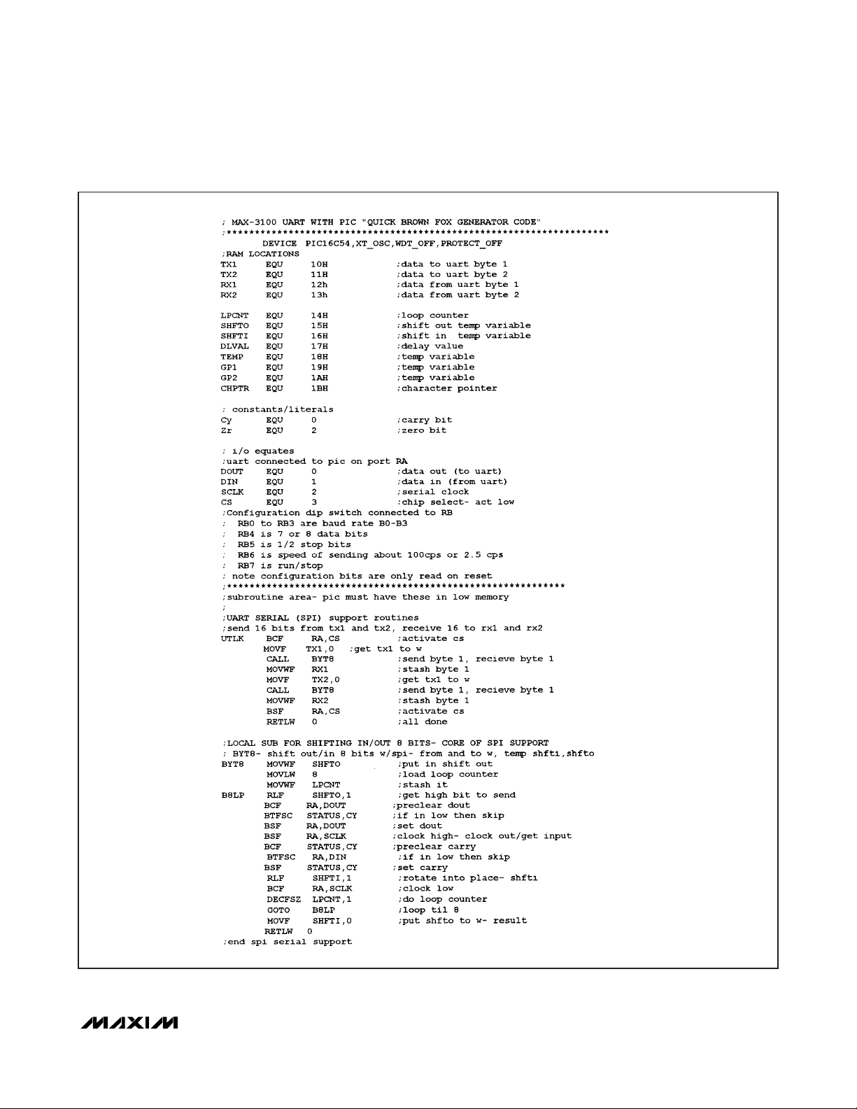
Figure 12b. MAX3100 Using PIC µC
MAX3100
SPI/MICROWIRE-Compatible
UART in QSOP-16
______________________________________________________________________________________ 21
Page 22

MAX3100
SPI/MICROWIRE-Compatible
UART in QSOP-16
22 ______________________________________________________________________________________
Figure 12b. MAX3100 Using PIC µC (continued)
Page 23

___________________________________________________Typical Operating Circuit
MAX3100
SPI/MICROWIRE-Compatible
UART in QSOP-16
______________________________________________________________________________________ 23
___________________Chip Information
PROCESS: BiCMOS
SUBSTRATE CONNECTED TO GND
PACKAGE TYPE PACKAGE CODE DOCUMENT NO.
14 Plastic DIP P14-3
21-0043
16 QSOP E16-1
21-0055
24 TQFN-EP T2444-4
21-0139
Package Information
For the latest package outline information and land patterns, go
to www.maxim-ic.com/packages
.
MAX3223
RS-232 I/O
μC
SPI/MICROWIRE
C1
DOUT
SCLK
CS
IRQ
MAX3100
TXDIN
RX
CTS
RTS
C2
Page 24

Maxim cannot assume responsibility for use of any circuitry other than circuitry entirely embodied in a Maxim product. No circuit patent licenses are
implied. Maxim reserves the right to change the circuitry and specifications without notice at any time.
24
____________________Maxim Integrated Products, 120 San Gabriel Drive, Sunnyvale, CA 94086 408-737-7600
© 2009 Maxim Integrated Products Maxim is a registered trademark of Maxim Integrated Products, Inc.
MAX3100
SPI/MICROWIRE-Compatible
UART in QSOP-16
Revision History
REVISION
NUMBER
1 12/01 Changed pin labeling 17
2 1/09 Added 24 TQFN information 1, 2, 5, 24
REVISION
DATE
DESCRIPTION
PAGES
CHANGED
 Loading...