

Page 1
General Description
The MAX3097E/MAX3098E feature three high-speed RS485/RS-422 receivers with fault-detection circuitry and
fault-status outputs. The receivers’ inputs have fault
thresholds that detect when the part is not in a valid state.
The MAX3097E/MAX3098E indicate when a receiver
input is in an open-circuit condition, short-circuit condition, or outside the common-mode range. They also
generate a fault indication when the differential input
voltage goes below a preset threshold. See Ordering
Information or the Electrical Characteristics for threshold values.
The fault circuitry includes a capacitor-programmable
delay to ensure that there are no erroneous fault conditions even at slow edge rates. Each receiver is capable
of accepting data at rates up to 32Mbps.
________________________Applications
RS-485/RS-422 Receivers for Motor-Shaft
Encoders
High-Speed, Triple RS-485/RS-422 Receiver with
Extended Electrostatic Discharge (ESD)
Triple RS-485/RS-422 Receiver with Input Fault
Indication
Telecommunications
Embedded Systems
Features
♦ Detects the Following RS-485 Faults:
Open-Circuit Condition
Short-Circuit Condition
Low Differential Voltage Signal
Common-Mode Range Violation
♦ ESD Protection
±15kV—Human Body Model
±15kV—IEC 1000-4-2, Air-Gap Discharge
Method
±8kV—IEC 1000-4-2, Contact Discharge Method
♦ Single +3V to +5.5V Operation
♦ -10V to +13.2V Extended Common-Mode Range
♦ Capacitor-Programmable Delay of Fault Indication
Allows Error-Free Operation at Slow Data Rates
♦ Independent and Universal Fault Outputs
♦ 32Mbps Data Rate
♦ 16-Pin QSOP is 40% Smaller than Industry-
Standard 26LS31/32 Solutions
MAX3097E/MAX3098E
±15kV ESD-Protected, 32Mbps, 3V/5V,
Triple RS-422/RS-485 Receivers with Fault Detection
________________________________________________________________ Maxim Integrated Products 1
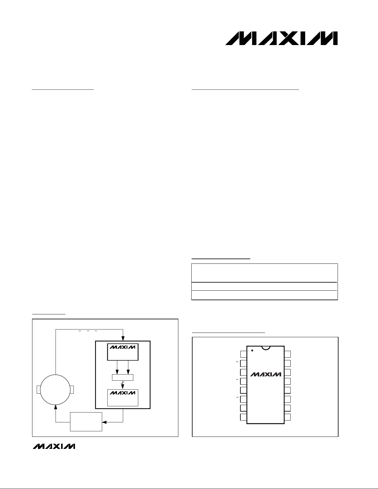
Pin Configuration
ENCODED SIGNALS
A, A, B, B, Z, Z
MOTOR DRIVER
MOTOR
MOTOR
CONTROLLER
ALARM
OUTPUTS
RECEIVER
OUTPUTS
DSP
8
MAX3097E
MAX3098E
MAX547
12-BIT D/A
Typical Application Circuit
19-1727; Rev 0; 7/00
For free samples and the latest literature, visit www.maxim-ic.com or phone 1-800-998-8800.
For small orders, phone 1-800-835-8769.
Ordering Information
Ordering Information continued at end of data sheet.
PART TEMP. RANGE
MAX3097ECEE 0°C to +70°C 16 QSOP
MAX3097ECSE 0°C to +70°C 16 SO
PINPACKAGE
TOP VIEW
1
AV
A
2
B
GND
DELAY
3
4
B
Z
5
Z
6
7
8
QSOP/SO/DIP
MAX3097E
MAX3098E
16
15
14
13
12
11
10
9
CC
ALARMA
OUTA
ALARMB
OUTB
ALARMZ
OUTZ
ALARMD
Page 2
MAX3097E/MAX3098E
±15kV ESD-Protected, 32Mbps, 3V/5V,
Triple RS-422/RS-485 Receivers with Fault Detection
2 _______________________________________________________________________________________
ABSOLUTE MAXIMUM RATINGS
ELECTRICAL CHARACTERISTICS
(VCC= +3V to +5.5V, TA= T
MIN
to T
MAX
, unless otherwise noted. Typical values are at VCC= +5V and TA = +25°C.)
Stresses beyond those listed under “Absolute Maximum Ratings” may cause permanent damage to the device. These are stress ratings only, and functional
operation of the device at these or any other conditions beyond those indicated in the operational sections of the specifications is not implied. Exposure to
absolute maximum rating conditions for extended periods may affect device reliability.
Supply Voltage (VCC).............................................................+7V
Receiver Input Voltage (A, A, B, B, Z, Z) .............................±25V
Output Voltage (OUT_, ALARM_)...............-0.3V to (V
CC
+ 0.3V)
DELAY ........................................................-0.3V to (V
CC
+ 0.3V)
Continuous Power Dissipation (T
A
= +70°C)
16-Pin QSOP (derate 8.3mW/°C above +70°C)............667mW
16-Pin SO (derate 8.7mW/°C above +70°C).................696mW
16-Pin Plastic DIP (derate 10.53mW/°C
above +70°C).............................................................762mW
Operating Temperature Ranges
MAX3097EC_E...................................................0°C to +70°C
MAX3098E_C_E.................................................0°C to +70°C
MAX3097E_E_E ..............................................-40°C to +85°C
MAX3098E_E_E ..............................................-40°C to +85°C
Storage Temperature Range .............................-65°C to +150°C
Junction Temperature......................................................+150°C
Lead Temperature (soldering, 10s) .................................+300°C
PARAMETER SYMBOL CONDITIONS MIN TYP MAX UNITS
Supply Voltage Range V
Supply Current I
Receiver Differential Threshold
Voltage (Note 1)
Receiver Input Hysteresis ∆V
Output High Voltage V
Output Low Voltage V
Receiver Input Resistance R
Input Current
(A , A , B , B (Z , Z )
Output Short-Circuit Current I
FAULT DETECTION
MAX3097E Fault-Detection
Receiver Differential Threshold
Voltage (Note 3)
MAX3098EA Fault-Detection
Receiver Differential Threshold
Voltage (Note 3)
CC
No load 3.1 4.0 mA
-10V ≤ VCM ≤ 13.2V -200 +200 mV
-10V ≤ VCM ≤ 13.2V 40 mV
TH
VCC = 4.75V, IO = -4mA, VID = 200mV V
VCC = 3.0V, IO = -1mA, VID = 200mV VCC - 1.0
VCC = 4.75V, IO = +4mA, VID = -200mV 0.4
VCC = 3.0V, IO = +1mA, VID = -200mV 0.4
-10V ≤ V
IN
≤ 13.2V 90 160 kΩ
CM
VCC = 0 or 5.5V
RO
≤ V
CC
0 ≤ V
V
F
CC
TH
OH
OL
I
IN
OSR
DIFH
VCM = 0
F
DIFL
F
DIFH
VCM = 0
F
DIFL
3 5.5 V
- 1.5
CC
V
= 13.2V
IN
(Note 2)
= -10V
V
IN
(Note 2)
0.07 0.14
-0.05 -0.11
±105 mA
High limit 275 475
Low limit -475 -275
High limit 0.12 0.20
Low limit -0.20 -0.12
V
V
mA
mV
V
Page 3
MAX3097E/MAX3098E
±15kV ESD-Protected, 32Mbps, 3V/5V,
Triple RS-422/RS-485 Receivers with Fault Detection
_______________________________________________________________________________________ 3
ELECTRICAL CHARACTERISTICS (continued)
(VCC= +3V to +5.5V, TA= T
MIN
to T
MAX
, unless otherwise noted. Typical values are at VCC= +5V and TA = +25°C.)
SWITCHING CHARACTERISTICS
(VCC= +3V to +5.5V, VID= ±3.0V, TA= T
MIN
to T
MAX
, unless otherwise noted. Typical values are at VCC= +5V and TA = +25°C.)
Note 1: VCMis the common-mode input voltage. VIDis the differential input voltage.
Note 2: V
IN
is the input voltage at pins A, A, B, B, Z, Z.
Note 3: A differential terminating resistor is required for proper function of open-circuit fault detection (see Applications Information).
Note 4: See Applications Information for a discussion of the receiver common-mode voltage range and the operating conditions for
fault indication.
Note 5: Applies to the individual channel immediate-fault outputs (ALARM_) and the general delayed-fault output (ALARMD) when
there is no external capacitor at DELAY.
Note 6: Equivalent pulse test: 1.3V / (t
DFLH
- t
DFHL
) ≥ SRD.
Note 7: Equivalent pulse test: 0.62V / (t
DFLH
- t
DFHL
) ≥ SRD.
MAX3098EB Fault-Detection
Receiver Differential Threshold
Voltage (Note 3)
Fault-Detection Common-Mode
Voltage Range (Note 4)
DELAY Current Source VCC = 5V, V
DELAY Threshold
ESD PROTECTION
ESD Protection
(A, A, B, B, Z, Z)
PARAMETER SYMBOL CONDITIONS MIN TYP MAX UNITS
F
F
F
F
DIFH
DIFL
CMH
CML
VCM = 0
High limit 13.2
Low limit -10
= 0 9 10 11 µA
DELAY
VCC = 3V 1.55 1.73 1.90
= 5V 3.1 3.29 3.5
V
CC
Human Body Model ±15
IEC1000-4-2 (Air-Gap Discharge) ±15
IEC1000-4-2 (Contact Discharge)
Propagation Delay from Input to
Output
Receiver Skew |t
Channel-to-Channel
Propagation Delay Skew
Maximum Data Rate f
FAULT DETECTION
Differential Fault Propagation
Delay to Output (Note 5)
PARAMETER SYMBOL CONDITIONS MIN TYP MAX UNITS
t
PLH
- t
PLH
|t
PHL
, t
SKEW
MAX
t
DFLH
t
DFHL
PHL
CL = 15pF,
Figures 1, 2
CL = 15pF, Figures 1, 2 ±10 ns
= 15pF, Figures 1, 2 ±10 ns
C
L
CL = 15pF, Figure 1 32 Mbps
CLF = 15pF, Figures 1, 3
High limit 70 250
Low limit -250 -70
±8
VCC = 4.5V to 5.5V 75
V
= 3.0V to 3.6V 85
CC
15
1.2
mV
V
V
kV
ns
µs
Minimum Differential Slew Rate
to Avoid False Alarm Output
Common-Mode Fault
Propagation Delay to Output
(Note 5)
t
CMFLH
t
CMFHL
MAX3097E (Note 6) 1.0
MAX3098E (Note 7) 0.33
CL = 15pF, Figures 1, 4
V/µs
15
µs
1.5
Page 4
DELAYED ALARM OUTPUT
MAX3097E/8E toc06
20µs/div
CH 1
CH 2
CH 3
GND
GND
GND
CH1: VA, 5V/div
CH2: V
ALARMA
, 5V/div
CH3: V
ALARMD
, 5V/div
V
A =
GND, C
DELAY
= 270pF
MAX3097E/MAX3098E
±15kV ESD-Protected, 32Mbps, 3V/5V,
Triple RS-422/RS-485 Receivers with Fault Detection
4 _______________________________________________________________________________________
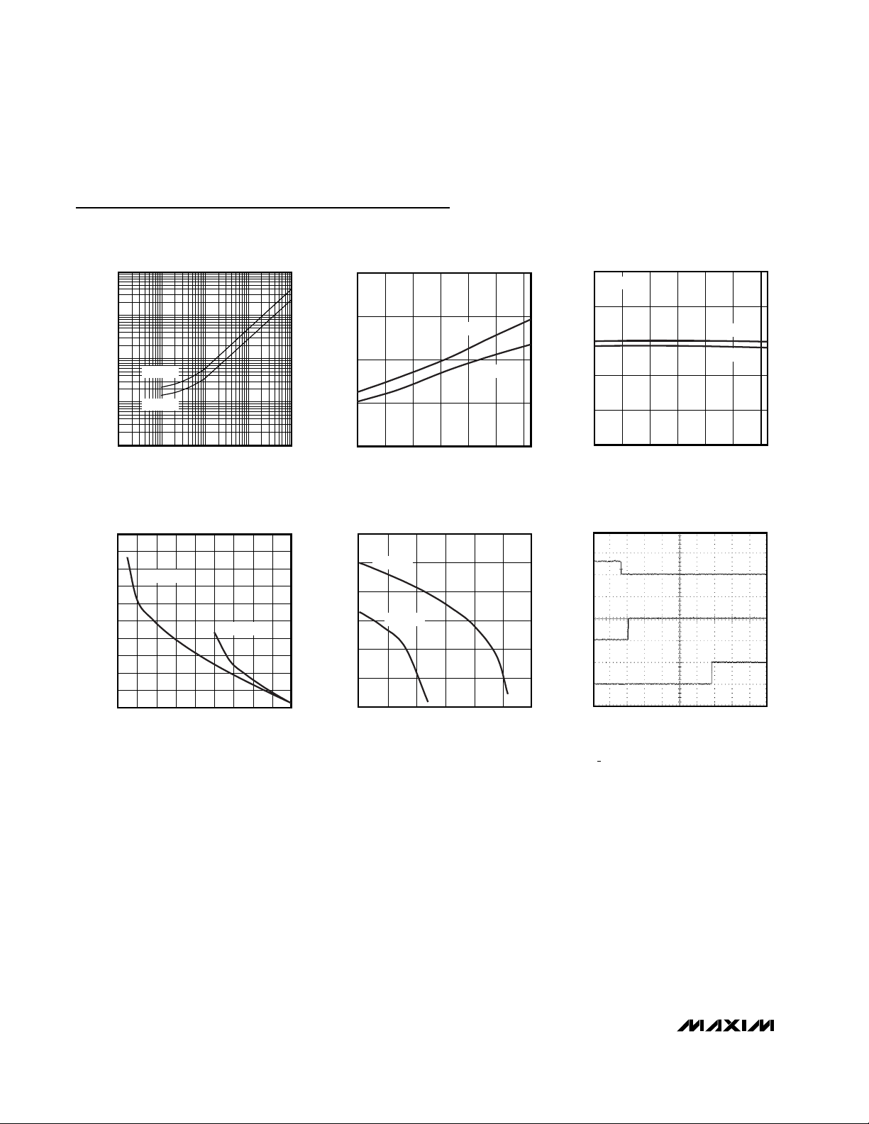
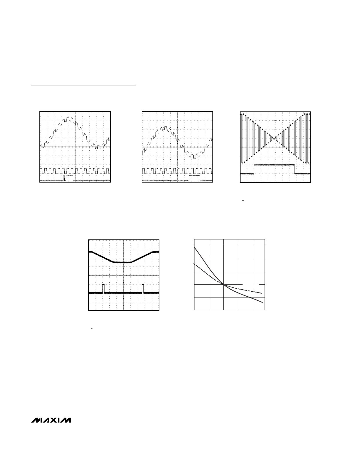
Typical Operating Characteristics
(Typical values are at VCC= +5V and TA= +25°C.)
1
100
10
1000
10,000
1
10010 1000
10,000
ALARMD OUTPUT DELAY
vs. CAPACITANCE
MAX3097E/8Etoc01
CAPACITANCE (pF)
ALARMD OUTPUT DELAY (µs)
VCC = 5V
VCC = 3V
30
40
50
60
70
-40 0-20
20
40 60
RECEIVER PROPAGATION DELAY
vs. TEMPERATURE
MAX3097E/8E toc02
TEMPERATURE (°C)
RECEIVER PROPAGATION DELAY (ns)
80
VCC = 5.0V
VCC = 3.3V
0
1
3
2
4
5
SUPPLY CURRENT vs.
TEMPERATURE
MAX3097E/8E toc03
SUPPLY CURRENT (mA)
-40 0-20
20
40 60
TEMPERATURE (°C)
80
VCC = 5.0V
VCC = 3.3V
NO LOAD
0
0.5
1.0
1.5
2.0
2.5
3.5
3.0
4.5
4.0
5.0
-45 -35-40 -30 -25 -20 -15 -10 -5 0
RECEIVER OUTPUT LOW VOLTAGE
vs. OUTPUT CURRENT
MAX3097E/8E toc04
OUTPUT CURRENT (mA)
OUTPUT LOW VOLTAGE (V)
VCC = 5.0V
VCC = 3.3V
0
1
2
4
3
5
6
010515203025
RECEIVER OUTPUT HIGH VOLTAGE
vs. OUTPUT CURRENT
MAX3097E/8E toc05
OUTPUT CURRENT (mA)
OUTPUT HIGH VOLTAGE (V)
VCC = 5.0V
VCC = 3.3V
Page 5
MAX3097E/MAX3098E
±15kV ESD-Protected, 32Mbps, 3V/5V,
Triple RS-422/RS-485 Receivers with Fault Detection
_______________________________________________________________________________________ 5
Typical Operating Characteristics (continued)
(Typical values are at VCC= +5V and TA= +25°C.)
MAX3097E
LOW DIFFERENTIAL INPUT FAULT
MAX3097E/8E toc08
CH 2 GND
GND
CH 1
100µs/div
CH1: V
A
, 200mV/div
CH2: V
ALARMA
, 5V/div
V
A =
GND
SLEW-RATE FAULT
MAX3097E/8E toc09
CH 2 GND
GND
CH 1
CH1: V
A
, 5V/div
CH2: V
ALARMA
, 5V/div
SLEW RATE = 0.05V/µs
V
A =
GND
-8
-4
4
0
8
12
-10 0-5 5 10
FAULT-DETECTION RECEIVER DIFFERENTIAL
THRESHOLD VOLTAGE SHIFT vs.
COMMON-MODE VOLTAGE
MAX3097E/8E toc10
COMMON-MODE VOLTAGE (V)
THRESHOLD SHIFT (mV)
MAX3097E
MAX3098E
COMMON-MODE VOLTAGE FAULT
(HIGH SIDE)
COMMON-MODE VOLTAGE FAULT
(LOW SIDE)
CH 1
CH 2
CH 3
CH1: VA + AC(60Hz), 10V/div
CH2: V
OUTA
CH3: V
ALARMA
3V
V
CC =
, 5V/div
, 5V/div
2ms/div
MAX3097E/8E toc07a
GND
GND
GND
CH 1
CH 2
CH 3
CH1: V
CH2: V
CH3: V
V
CC =
A
OUTA
ALARMA
3V
, 5V/div
, 5V/div
2ms/div
+ AC(60Hz), 10V/div
MAX3097E/8E toc07b
GND
GND
GND
Page 6

MAX3097E/MAX3098E
±15kV ESD-Protected, 32Mbps, 3V/5V,
Triple RS-422/RS-485 Receivers with Fault Detection
6 _______________________________________________________________________________________
Pin Description
PIN NAME FUNCTION
1 A Noninverting Receiver A Input
2 A Inverting Receiver A Input
3 B Noninverting Receiver B Input
4 B Inverting Receiver B Input
5 Z Noninverting Receiver Z Input
6 Z Inverting Receiver Z Input
7 GND Ground
Programmable Delay Terminal. Connect a capacitor from DELAY to GND to set the
8 DELAY
9 ALARMD
ALARMD output delay time. To obtain a minimum delay, leave DELAY unconnected. See
Capacitance vs. ALARMD Output Delay in the Typical Operating Characteristics.
Delayed Fault Output. This output is the logic OR of ALARMA, ALARMB, and ALARMZ.
Place a capacitor from the DELAY pin to GND to set the delay (see Setting Delay Time). A
high logic level indicates a fault condition on at least one receiver input pair. A low level on
this pin indicates no fault condition is present.
Z Receiver Output. If V
10 OUTZ
11 ALARMZ
be low. If Z or Z exceeds the receiver’s input common-mode voltage range, the ALARMZ
output will be high and OUTZ will be indeterminate.
Z Fault Output. When ALARMZ is high, OUTZ is indeterminate. Tables 1 and 2 show all the
possible states for which an alarm is set.
- V Z ≥ +200mV, OUTZ will be high. If VZ - V Z ≤ -200mV, OUTZ will
Z
B Receiver Output. If V
12 OUTB
13 ALARMB
14 OUTA
15 ALARMA
16 V
CC
be low. If B or B exceeds the input receiver’s common-mode voltage range, the ALARMB
output will be high and OUTB will be indeterminate.
B Fault Output. When ALARMB is high, OUTB is indeterminate. Tables 1 and 2 show all the
possible states for which an alarm is set.
A Receiver Output. If V
be low. If A or A exceeds the receiver’s input common-mode voltage range, the ALARMA
output will be high and OUTA will be indeterminate.
A Fault Output. When ALARMA is high, OUTA is indeterminate. Tables 1 and 2 show all the
possible states for which an alarm is set.
Power Supply
- V B ≥ +200mV, OUTB will be high. If VB - V B ≤ -200mV, OUTB will
B
- V A ≥ +200mV, OUTA will be high. If VA - V A ≤ -200mV, OUTA will
A
Page 7

MAX3097E/MAX3098E
±15kV ESD-Protected, 32Mbps, 3V/5V,
Triple RS-422/RS-485 Receivers with Fault Detection
_______________________________________________________________________________________ 7
Figure 1. Typical Receiver Test Circuit
Figure 2. Propagation Delay
Figure 3. Fault-Detection Timing
Figure 4. Common-Mode Fault Propagation Delay
Test Circuits and Waveforms
Detailed Description
The MAX3097E/MAX3098E feature high-speed, triple
RS-485/RS-422 receivers with fault-detection circuitry
and fault-status outputs. The fault outputs are active
push-pull, requiring no pull-up resistors. The fault circuitry includes a capacitor-programmable delayed
FAULT_ output to ensure that there are no erroneous
fault conditions even at slow edge rates (see Delayed
Fault Output). The receivers operate at data rates up to
32Mbps.
The MAX3097E/MAX3098E are designed for motorshaft encoders with standard A, B, and Z outputs (see
Using the MAX3097E/MAX3098E as Shaft Encoder
Receivers). The devices provide an alarm for open-cir-
cuit conditions, short-circuit conditions, data nearing
the minimum differential threshold conditions, data
below the minimum threshold conditions, and receiver
inputs outside the input common-mode range. Tables 1
and 2 are functional tables for each receiver.
ALARMA
(FAULT OUTPUT)
OR
ALARMD
C
A
V
A
V
ID
A
V
A
LF
OUTA
C
L
+3V
V
ID
-3V
V
OH
R
O
V
OL
OV OV
t
PLH
RISE/FALL TIMES ≤2ns
t
PHL
V
/2VCC/2
CC
F
DIFH
V
ID
-3.0V
ALARM OR ALARMD
OV
F
DIFL
t
V
OH
V
OL
DFLH
t
DFHL
F
CMH
V
+3.0V
VCC/2VCC/2
IN
OV
F
CML
t
CMFLH
V
OH
ALARM OR ALARMD
V
OL
VCC/2
t
CMFHL
t
t
CMFLH
CMFHL
/2
V
CC
VCC/2
/2
V
CC
Page 8

MAX3097E/MAX3098E
±15kV ESD-Protected, 32Mbps, 3V/5V,
Triple RS-422/RS-485 Receivers with Fault Detection
8 _______________________________________________________________________________________
Note 1: ALARMD indicates fault for any receiver.
Note 2: Receiver output may oscillate with this differential input condition.
Note 3: See Applications Information for conditions leading to input range fault condition.
X = Don’t care
Table 1. MAX3097E Alarm Function Table (Each Receiver)
Table 2. MAX3098EA Alarm Function Table (Each Receiver)
Note 1: ALARMD indicates fault for any receiver.
Note 2: Receiver output may oscillate with this differential input condition.
Note 3: See Applications Information for conditions leading to input range fault condition.
X = Don’t care; for B-grade functionality, replace V
ID
input values in Table 2 with B-grade parameters from Electrical Characteristics.
V
(DIFFERENTIAL
INPUT VOLTAGE)
≥0.475V 1 0 0 Normal Operation
<0.475V and ≥0.275V 1 Indeterminate Indeterminate Indeterminate
<0.275V and ≥0.2V 1 1 1 Low Input Differential Voltage
≤0.2V and ≥-0.2V
≤-0.2V and >-0.275V 0 1 1 Low Input Differential Voltage
≤-0.275V and
>-0.475V
≤-0.475V
INPUTS OUTPUTS
ID
X <-10V or >+13.2V
COMMON-MODE
VOLTAGE
≤13.2V and ≥-10V
OUT_ ALARM_
Indeterminate
(Note 2)
0 Indeterminate Indeterminate
000
Indeterminate
(Note 3)
ALARMD
t ≥ DELAY
(NOTE 1)
1 1 Low Input Differential Voltage
11
FAULT CONDITION
Indeterminate
Outside Common-Mode
Voltage Range
V
(DIFFERENTIAL
INPUT VOLTAGE)
≥0.2V 1 0 0 Normal Operation
<0.2V and ≥0.12V
<0.12V and ≥ - 0.12V
≤-0.12V and ≥ -0.2V
≤-0.2V
INPUTS OUTPUTS
ID
X
COMMON-MODE
VOLTAGE
≤13.2V and ≥-
10V
<-10V or
>+13.2V
OUT_ ALARM_
Indeterminate
Indeterminate
(Note 2)
Indeterminate
0 0 0 Normal Operation
Indeterminate
(Note 3)
ALARMD
t ≥ DELAY
(NOTE 1)
Indeterminate Indeterminate Indeterminate
1 1 Low Input Differential Voltage
Indeterminate Indeterminate Indeterminate
11
FAULT CONDITION
Outside Common-Mode Voltage
Range
Page 9

MAX3097E/MAX3098E
±15kV ESD-Protected, 32Mbps, 3V/5V,
Triple RS-422/RS-485 Receivers with Fault Detection
_______________________________________________________________________________________ 9
±15kV ESD Protection
As with all Maxim devices, ESD-protection structures
are incorporated on all pins to protect against ESD
encountered during handling and assembly. The
MAX3097E/MAX3098E receiver inputs have extra protection against static electricity found in normal operation. Maxim’s engineers developed state-of-the-art
structures to protect these pins against ±15kV ESD
without damage. After an ESD event, the MAX3097E/
MAX3098E continue working without latchup.
ESD protection can be tested in several ways. The
receiver inputs are characterized for protection to the
following:
• ±15kV using the Human Body Model
• ±8kV using the Contact Discharge method specified
in IEC 1000-4-2 (formerly IEC 801-2)
• 15kV using the Air-Gap Discharge method specified
in IEC 1000-4-2 (formerly IEC 801-2)
ESD Test Conditions
ESD performance depends on a number of conditions.
Contact Maxim for a reliability report that documents
test setup, methodology, and results.
Human Body Model
Figure 5a shows the Human Body Model, and Figure
5b shows the current waveform it generates when discharged into a low impedance. This model consists of
a 100pF capacitor charged to the ESD voltage of interest, which is then discharged into the device through a
1.5kΩ resistor.
IEC 1000-4-2
Since January 1996, all equipment manufactured and/or
sold in the European community has been required to
meet the stringent IEC 1000-4-2 specification. The IEC
1000-4-2 standard covers ESD testing and performance
of finished equipment; it does not specifically refer to integrated circuits. The MAX3097E/MAX3098E help you
design equipment that meets Level 4 (the highest level)
of IEC 1000-4-2, without additional ESD-protection components.
The main difference between tests done using the
Human Body Model and IEC 1000-4-2 is higher peak
current in IEC 1000-4-2. Because series resistance is
lower in the IEC 1000-4-2 ESD test model (Figure 6a), the
ESD-withstand voltage measured to this standard is generally lower than that measured using the Human Body
Model. Figure 6b shows the current waveform for the
±8kV IEC 1000-4-2 Level 4 ESD Contact Discharge test.
The Air-Gap test involves approaching the device with a
charge probe. The Contact Discharge method connects
the probe to the device before the probe is energized.
Machine Model
The Machine Model for ESD testing uses a 200pF storage capacitor and zero-discharge resistance. It mimics
the stress caused by handling during manufacturing
and assembly. All pins (not just RS-485 inputs) require
this protection during manufacturing. Therefore, the
Machine Model is less relevant to the I/O ports than are
the Human Body Model and IEC 1000-4-2.
Figure 5a. Human Body ESD Test Model
Figure 5b. Human Body Model Current Waveform
R
C
1MΩ
CHARGE-CURRENT
LIMIT RESISTOR
HIGH-
VOLTAGE
DC
SOURCE
C
s
100pF
R
D
1.5k
DISCHARGE
RESISTANCE
STORAGE
CAPACITOR
DEVICE
UNDER
TEST
IP 100%
90%
AMPERES
36.8%
10%
0
0
t
RL
TIME
t
DL
CURRENT WAVEFORM
PEAK-TO-PEAK RINGING
I
r
(NOT DRAWN TO SCALE)
Page 10

___________Applications Information
Using the MAX3097E/MAX3098E as Shaft
Encoder Receivers
The MAX3097E/MAX3098E are triple RS-485 receivers
designed for shaft encoder receiver applications. A
shaft encoder is an electromechanical transducer that
converts mechanical rotary motion into three RS-485
differential signals. Two signals, A (A and A) and B (B
and B) provide incremental pulses as the shaft turns,
while the index signal, Z (Z and Z) occurs only once
per revolution to allow synchronization of the shaft to a
known position. Digital signal processing (DSP) techniques are used to count the pulses and provide feedback of both shaft position and shaft velocity for a
stable positioning system.
Shaft encoders typically transmit RS-485 signals over
twisted-pair cables since the signal often has to travel
across a noisy electrical environment (Figure 7).
Detecting Faults
Signal integrity from the shaft encoder to the DSP is
essential for reliable system operation. Degraded signals could cause problems ranging from simple miscounts to loss of position. In an industrial environment,
many problems can occur within the three twisted
pairs. The MAX3097E/MAX3098E can detect various
types of common faults, including a low-input-level signal, open-circuit wires, short-circuit wires, and an input
signal outside the common-mode input voltage range
of the receiver.
Detecting Short Circuits
In Figure 8, if wires A and A are shorted together, then A
and A will be at the same potential, so the difference in
the voltage between the two will be approximately 0. This
causes fault A to trigger since the difference between A A is less than the differential fault threshold.
Detecting Open-Circuit Conditions
Detecting an open-circuit condition is similar to detecting a short-circuit condition and relies on the terminating resistor being across A and A. For example, if the
wire drops out of the A terminal, A pulls A through the
terminating resistor to look like the same signal. In this
condition, VIDis approximately 0 and a fault occurs.
MAX3097E/MAX3098E
±15kV ESD-Protected, 32Mbps, 3V/5V,
Triple RS-422/RS-485 Receivers with Fault Detection
10 ______________________________________________________________________________________
Figure 7. Typical Shaft Encoder Output
Figure 6a. IEC 1000-4-2 ESD Test Model
Figure 6b. IEC 1000-4-2 ESD Generator Current Waveform
R
C
50MΩ to 100MΩ
CHARGE-CURRENT
LIMIT RESISTOR
HIGH-
VOLTAGE
DC
SOURCE
100%
90%
PEAK
I
10%
tr = 0.7ns to 1ns
A
A
B
B
Z
Z
C
s
150pF
I
30ns
R
D
330Ω
DISCHARGE
RESISTANCE
STORAGE
CAPACITOR
60ns
DEVICE
UNDER
TEST
t
Page 11

MAX3097E/MAX3098E
±15kV ESD-Protected, 32Mbps, 3V/5V,
Triple RS-422/RS-485 Receivers with Fault Detection
______________________________________________________________________________________ 11
Common-Mode Range
The MAX3097E/MAX3098E contain circuitry that detects if the input stage is going outside its useful common-mode range. If the received data could be
unreliable, a fault signal is triggered.
Detecting Low Input Differential
Due to cable attenuation on long wire runs, it is possible that VID< 200mV, and incorrect data will be
received. In this condition, a fault will be indicated.
Delayed Fault Output
The delayed fault output provides a programmable
blanking delay to allow transient faults to occur without
triggering an alarm. Such faults may occur with slow
signals triggering the receiver alarm through the zero
crossover region.
Figure 9 shows the delayed alarm output.
ALARMD performs a logic OR of ALARMA, ALARMB,
and ALARMZ (Figure 10). A NOR gate drives an Nchannel MOSFET so that in normal operation with no
faults, the current source (10µA typ) is shunted to
ground. Upon activation of any alarm from receiver A,
B, or Z, the MOSFET is turned off, allowing the current
source to charge C
DELAY
. When V
DELAY
exceeds the
DELAY threshold, the comparator output, ALARMD,
goes high. ALARMD is reset when all receiver alarms
go low, quickly discharging C
DELAY
to ground.
Setting Delay Time
ALARMD’s delay time is set with a single capacitor
connected from DELAY to GND. The delay comparator
threshold varies with supply voltage, and the C
DELAY
value can be determined for a given time delay period
from the Capacitance vs. ALARMD Output Delay graph
in the Typical Operating Characteristics or using the
following equations:
tD= 15 + 0.33 x C
DELAY
(for VCC= 5V)
and
tD= 10 + 0.187 x C
DELAY
(for VCC= 3V)
where tDis in µs and C
DELAY
is in pF.
Figure 9. Delayed Alarm Output
Figure 10. ALARMD Simplified Schematic
Figure 8. Short-Circuit Detection
A
A
NORMAL OPERATION SHORT CIRCUIT A TO A
ALARMA
ALARMB
t
ALARMD
DELAY
CURRENT
SOURCE
ALARMA
ALARMB
ALARMZ
ALARM_
DELAY
ALARMD
D
t
D
*The capacitor (C
If the duration of an ALARM_ pulse is less than t
output will be present at ALARMD.
NMOS
G1
) charges up slowly, but discharges rapidly.
DELAY
C
DELAY
(EXTERNAL)
t
DLY
*
DELAY
COMPARATOR
ALARMD
DELAY THRESHOLD
, no alarm
DLY
Page 12
MAX3097E/MAX3098E
±15kV ESD-Protected, 32Mbps, 3V/5V,
Triple RS-422/RS-485 Receivers with Fault Detection
12 ______________________________________________________________________________________
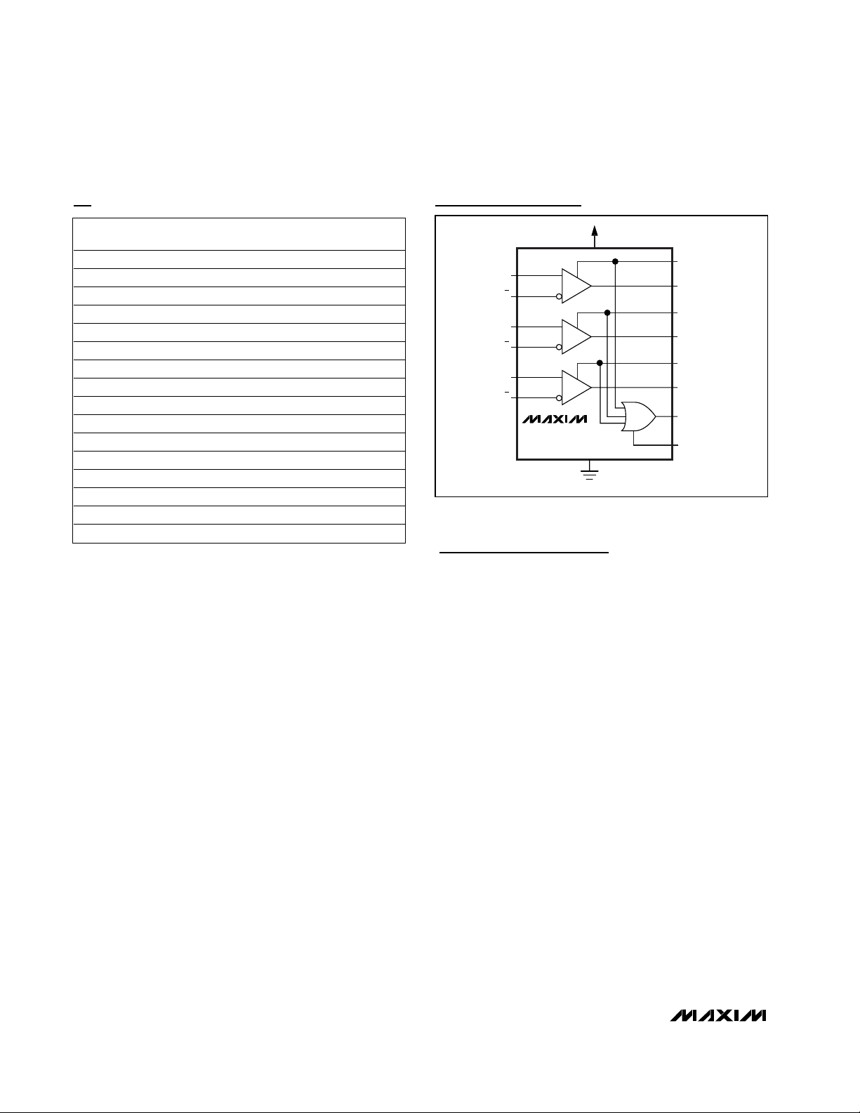
Functional Diagram
Chip Information
TRANSISTOR COUNT: 675
PROCESS: CMOS
Ordering Information (continued)
PART
TEMP. RANGE
PINPACKAGE
MAX3097ECPE 0°C to +70°C 16 Plastic DIP
MAX3097EEEE -40°C to +85°C 16 QSOP
MAX3097EESE -40°C to +85°C 16 SO
MAX3097EEPE -40°C to +85°C 16 Plastic DIP
MAX3098EACEE 0°C to +70°C 16 QSOP
MAX3098EACSE 0°C to +70°C 16 SO
MAX3098EACPE 0°C to +70°C 16 Plastic DIP
MAX3098EAEEE -40°C to +85°C 16 QSOP
MAX3098EAESE -40°C to +85°C 16 SO
MAX3098EAEPE -40°C to +85°C 16 Plastic DIP
MAX3098EBCEE 0°C to +70°C 16 QSOP
MAX3098EBCSE 0°C to +70°C 16 SO
MAX3098EBCPE 0°C to +70°C 16 Plastic DIP
MAX3098EBEEE -40°C to +85°C 16 QSOP
MAX3098EBESE -40°C to +85°C 16 SO
MAX3098EBEPE
-40°C to +85°C 16 Plastic DIP
A
A
B
B
Z
Z
MAX3097E
MAX3098E
V
CC
ALARMA
OUTA
ALARMB
OUTB
ALARMZ
OUTZ
ALARMD
DELAY
GND
Page 13

MAX3097E/MAX3098E
±15kV ESD-Protected, 32Mbps, 3V/5V,
Triple RS-422/RS-485 Receivers with Fault Detection
______________________________________________________________________________________ 13
Package Information
SOICN.EPS
Page 14

MAX3097E/MAX3098E
±15kV ESD-Protected, 32Mbps, 3V/5V,
Triple RS-422/RS-485 Receivers with Fault Detection
14 ______________________________________________________________________________________
Package Information (continued)
QSOP.EPS
Page 15

MAX3097E/MAX3098E
±15kV ESD-Protected, 32Mbps, 3V/5V,
Triple RS-422/RS-485 Receivers with Fault Detection
______________________________________________________________________________________ 15
Package Information (continued)
PDIPN.EPS
Page 16

MAX3097E/MAX3098E
±15kV ESD-Protected, 32Mbps, 3V/5V,
Triple RS-422/RS-485 Receivers with Fault Detection
Maxim cannot assume responsibility for use of any circuitry other than circuitry entirely embodied in a Maxim product. No circuit patent licenses are
implied. Maxim reserves the right to change the circuitry and specifications without notice at any time.
16 ____________________Maxim Integrated Products, 120 San Gabriel Drive, Sunnyvale, CA 94086 408-737-7600
© 2000 Maxim Integrated Products Printed USA is a registered trademark of Maxim Integrated Products.
NOTES
 Loading...