

Page 1
________________General Description
The MAX3095/MAX3096 are rugged, low-power, quad,
RS-422/RS-485 receivers with electrostatic discharge
(ESD) protection for use in harsh environments. All
receiver inputs are protected to ±15kV using IEC 10004-2 Air-Gap Discharge, ±8kV using IEC 1000-4-2 Contact
Discharge, and ±15kV using the Human Body Model.
The MAX3095 operates from a +5V supply, while the
MAX3096 operates from a +3.3V supply. Receiver propagation delays are guaranteed to within ±8ns of a predetermined value, thereby ensuring device-to-device
matching across production lots.
Complementary enable inputs can be used to place the
devices in a 1nA low-power shutdown mode in which
the receiver outputs are high impedance. When active,
these receivers have a fail-safe feature that guarantees
a logic-high output if the input is open circuit. They also
feature a quarter-unit-load input impedance that allows
128 receivers on a bus.
The MAX3095/MAX3096 are pin-compatible, low-power
upgrades to the industry-standard ’26LS32. They are
available in a space-saving QSOP package.
________________________Applications
Telecommunications Equipment
Rugged RS-422/RS-485/RS-423 Bus Receiver
Receivers for ESD-Sensitive Applications
Level Translators
____________________________Features
♦♦
ESD Protection:
±15kV—IEC 1000-4-2, Air-Gap Discharge
±8kV—IEC 1000-4-2, Contact Discharge
±15kV—Human Body Model
♦♦
Guaranteed Propagation-Delay Tolerance
Between All ICs:
±8ns (MAX3095)
±10ns (MAX3096)
♦♦
Single +3V Operation (MAX3096)
Single +5V Operation (MAX3095)
♦♦
16-Pin QSOP (8-pin SO footprint)
♦♦
10Mbps Data Rate
♦♦
Allow up to 128 Receivers on the Bus
♦♦
1nA Low-Power Shutdown Mode
♦♦
2.4mA Operating Supply Current
♦♦
Pin-Compatible Upgrades to ’26LS32
MAX3095/MAX3096
±15kV ESD-Protected, 10Mbps, 3V/5V,
Quad RS-422/RS-485 Receivers
________________________________________________________________
Maxim Integrated Products
1
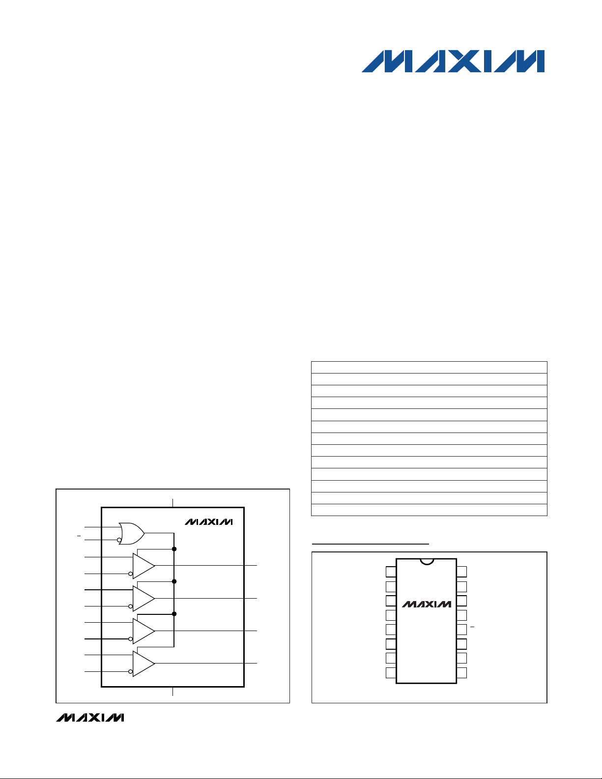
Pin Configuration
Y1
Y2
Y3
Y4
A1
B1
A2
B2
A3
B3
A4
B4
MAX3095
MAX3096
V
CC
GND
G
G
________________Functional Diagram
19-0498; Rev 3; 1/10
PART
MAX3095CPE+
MAX3095CSE+
MAX3095CEE+ 0°C to +70°C
0°C to +70°C
0°C to +70°C
TEMP. RANGE PIN-PACKAGE
16 Plastic DIP
16 Narrow SO
16 QSOP
_______________Ordering Information
MAX3095EPE+
MAX3095ESE+
MAX3095EEE+ -40°C to +85°C
-40°C to +85°C
-40°C to +85°C 16 Plastic DIP
16 Narrow SO
16 QSOP
MAX3096CPE+
MAX3096CSE+
MAX3096CEE+ 0°C to +70°C
0°C to +70°C
0°C to +70°C 16 Plastic DIP
16 Narrow SO
16 QSOP
MAX3096EPE+
MAX3096ESE+
MAX3096EEE+ -40°C to +85°C
-40°C to +85°C
-40°C to +85°C 16 Plastic DIP
16 Narrow SO
16 QSOP
For pricing, delivery, and ordering information, please contact Maxim Direct at 1-888-629-4642,
or visit Maxim’s website at www.maxim-ic.com.
+
Denotes a lead(Pb)-free/RoHS-compliant package.
TOP VIEW
GND
+
1
B1 V
A1
2
Y1
3
MAX3095
4
G
Y2
A2
B2
MAX3096
5
6
7
8
DIP/SO/QSOP
16
15
14
13
12
11
10
9
CC
B4
A4
Y4
G
Y3
A3
B3
Page 2
MAX3095/MAX3096
±15kV ESD-Protected, 10Mbps, 3V/5V,
Quad RS-422/RS-485 Receivers
2 _______________________________________________________________________________________
ABSOLUTE MAXIMUM RATINGS
DC ELECTRICAL CHARACTERISTICS—MAX3095
(VCC= 5V ±5%, TA= T
MIN
to T
MAX
, unless otherwise noted. Typical values are at TA= +25°C.) (Note 1)
Stresses beyond those listed under “Absolute Maximum Ratings” may cause permanent damage to the device. These are stress ratings only, and functional
operation of the device at these or any other conditions beyond those indicated in the operational sections of the specifications is not implied. Exposure to
absolute maximum rating conditions for extended periods may affect device reliability.
Supply Voltage (VCC)...............................................................7V
Control Input Voltage (G, G).......................-0.3V to (V
CC
+ 0.3V)
Receiver Input Voltage (A_, B_)...........................................±25V
Receiver Output Voltage (Y_).....................-0.3V to (V
CC
+ 0.3V)
Continuous Power Dissipation (T
A
= +70°C)
16-Pin Plastic DIP (derate 10.5mW/°C above +70°C) .762mW
16-Pin SO (derate 8.7mW/°C above +70°C)................696mW
16-Pin QSOP (derate 8.3mW/°C above +70°C)...........667mW
Operating Temperature Ranges
MAX309_C_ _ .....................................................0°C to +70°C
MAX309_E_ _...................................................-40°C to +85°C
Storage Temperature Range .............................-65°C to +160°C
Lead Temperature (soldering, 10s) .................................+300°C
VCM= 0V
IEC 1000-4-2 (Contact Discharge)
-7V ≤ VCM≤ 12V
IEC 1000-4-2 (Air-Gap Discharge)
Human Body Model
-7V ≤ VCM≤ 12V
0 ≤ V
OUT
≤ VCC, G = VCCor G = GND
0 ≤ V
OUT
≤ VCC, G = GND and G = V
CC
I
OUT
= 4mA, VID= -200mV,
G = V
CC
or G = GND, Figure 1
G = GND and G = V
CC
I
OUT
= -4mA, VID= 200mV,
G = V
CC
or G = GND, Figure 1
No load, G = VCCor G = GND
CONDITIONS
±8
±15
kV
±15
ESD Protection
(Note 2)
µA0.001 10
mA2.4 3.5
I
CC
Supply Current
mV45
mV-200 200V
TH
Receiver Differential Input
Threshold
Receiver Input Hysteresis
kΩ48R
IN
Receiver Input Resistance
mA±7 ±75I
OSR
Output Short-Circuit Current
µA±1I
OZR
Three-State Current at Receiver
Output
V0.4V
OL
Receiver Output Low Voltage
µA±1
Enable Input Current (G, G)
V2.0V
IH
Enable Input High Voltage (G, G)
V0.8V
IL
Enable Input Low Voltage (G, G)
VVCC- 1.5V
OH
Receiver Output High Voltage
UNITSMIN TYP MAXSYMBOLPARAMETER
µA
250
I
IN
Receiver Input Current (A_, B_) VCC= 0V or 5.25V
VIN= 12V
-200VIN= -7V
Page 3
MAX3095/MAX3096
±15kV ESD-Protected, 10Mbps, 3V/5V,
Quad RS-422/RS-485 Receivers
_______________________________________________________________________________________ 3
DC ELECTRICAL CHARACTERISTICS—MAX3096
(VCC= 3.135V to 3.6V, TA= T
MIN
to T
MAX
, unless otherwise noted. Typical values are at VCC= 3.3V, TA= +25°C.) (Note 1)
SWITCHING CHARACTERISTICS—MAX3095
(VCC= 5V ±5%, TA= T
MIN
to T
MAX
, unless otherwise noted. Typical values are at TA= +25°C.)
VCC= 5V ±5%, TA= T
MIN
to T
MAX
Figure 3
Figure 3
|VID| = 3V, Figure 2, matched conditions
|VID| = 3V,
Figure 2
Figure 3
Figure 3
CONDITIONS
Mbps10f
MAX
Maximum Data Rate
ns60 100t
HZ
Output Disable Time from
High Level
ns60 100t
LZ
Output Disable Time from
Low Level
78 86 94
ns
65 98
t
PLH
, t
PHL
Input-to-Output Propagation
Delay
ns600 800t
ZH
Output Enable Time to
High Level
ns600 800t
ZL
Output Enable Time to
Low Level
ns16
Device-to-Device PropagationDelay Matching
68 76 84
71 79 87
65 73 81
82 90 98
74 82 90
UNITSMIN TYP MAXSYMBOLPARAMETER
VCM= 0V
-7V ≤ VCM≤ 12V
-7V ≤ VCM≤ 12V
0 ≤ V
OUT
≤ VCC, G = VCCor G = GND
0 ≤ V
OUT
≤ VCC, G = GND and G = V
CC
I
OUT
= 2.5mA, VID= -200mV,
G = V
CC
or G = GND, Figure 1
I
OUT
= -1.5mA, VID= 200mV,
G = V
CC
or G = GND, Figure 1
CONDITIONS
mV45
mV-200 200V
TH
Receiver Differential Input
Threshold
Receiver Input Hysteresis
kΩ48R
IN
Receiver Input Resistance
mA±4 ±60I
OSR
Output Short-Circuit Current
µA±1I
OZR
Three-State Current at Receiver
Output
V0.4V
OL
Receiver Output Low Voltage
µA±1
Enable Input Current (G, G)
V2.0V
IH
Enable Input High Voltage (G, G)
V0.8V
IL
Enable Input Low Voltage (G, G)
VVCC- 0.4V
OH
Receiver Output High Voltage
UNITSMIN TYP MAXSYMBOLPARAMETER
µA
250
I
IN
Receiver Input Current (A_, B_) VCC= 0V or 3.6V
VIN= 12V
-200VIN= -7V
ns-4 ±10t
SK
Propagation-Delay Skew
(t
PLH
- t
PHL
)
TA= +85°C
TA= +25°C
TA= -40°C
TA= +85°C
TA= +25°C
TA= -40°C
VCC= 5.25V
VCC= 4.75V
Page 4
MAX3095/MAX3096
±15kV ESD-Protected, 10Mbps, 3V/5V,
Quad RS-422/RS-485 Receivers
4 _______________________________________________________________________________________
IEC 1000-4-2 (Contact Discharge)
IEC 1000-4-2 (Air-Gap Discharge)
Human Body Model
G = GND and G = V
CC
No load, G = VCCor G = GND
CONDITIONS
±8
±15
kV
±15
ESD Protection
(Note 2)
µA0.001 10
mA2.4 4.0
I
CC
Supply Current
UNITSMIN TYP MAXSYMBOLPARAMETER
DC ELECTRICAL CHARACTERISTICS—MAX3096 (continued)
(VCC= 3.135V to 3.6V, TA= T
MIN
to T
MAX
, unless otherwise noted. Typical values are at VCC= 3.3V, TA= +25°C.) (Note 1)
|VID| = 3V,
Figure 2
VCC= 3.135V to 3.6V, TA= T
MIN
to T
MAX
Figure 3
Figure 3
|VID| = 3V, Figure 2, matched conditions
Figure 3
Figure 3
CONDITIONS
Mbps10f
MAX
Maximum Data Rate
ns80 180t
HZ
Output Disable Time from
High Level
ns80 180t
LZ
Output Disable Time from
Low Level
88 98 112
ns
69 127
t
PLH
, t
PHL
Input-to-Output Propagation
Delay
ns600 1000t
ZH
Output Enable Time to
High Level
ns600 1000t
ZL
Output Enable Time to
Low Level
ns24
Device-to-Device PropagationDelay Matching
82 92 106
78 88 102
69 79 93
103 113 127
91 101 115
UNITSMIN TYP MAXSYMBOLPARAMETER
SWITCHING CHARACTERISTICS—MAX3096
(VCC= 3.135V to 3.6V, TA= T
MIN
to T
MAX
, unless otherwise noted. Typical values are at TA= +25°C.)
Note 1: All currents into the device are positive; all currents out of the device are negative. All voltages are referred to device
ground, unless otherwise noted.
Note 2: Receiver inputs (A_, B_).
ns-2 ±10t
SK
Propagation-Delay Skew
(t
PLH
- t
PHL
)
TA= +85°C
TA= +25°C
TA= -40°C
TA= +85°C
TA= +25°C
TA= -40°C
VCC= 3.60V
VCC= 3.135V
Page 5

MAX3095/MAX3096
±15kV ESD-Protected, 10Mbps, 3V/5V,
Quad RS-422/RS-485 Receivers
_______________________________________________________________________________________
5
Typical Operating Characteristics
(VCC= 5V for MAX3095, VCC= 3.3V for MAX3096, TA= +25°C, unless otherwise noted.)
OUTPUT CURRENT vs.
OUTPUT LOW VOLTAGE
-50
-40
-30
-20
OUTPUT CURRENT (mA)
-10
0
021 345
MAX3096
OUTPUT LOW VOLTAGE (V)
MAX3095
OUTPUT HIGH VOLTAGE
vs. TEMPERATURE
5
MAX3095
4
30
MAX3095-01
25
20
15
10
OUTPUT CURRENT (mA)
5
0
3.0
MAX3095-04
2.8
OUTPUT CURRENT vs.
OUTPUT HIGH VOLTAGE
MAX3095
MAX3096
021 345
OUTPUT HIGH VOLTAGE (V)
SUPPLY CURRENT vs. TEMPERATURE
1.0
I
0.9
MAX3095-02
0.8
0.7
0.6
0.5
0.4
0.3
OUTPUT LOW VOLTAGE (V)
0.2
0.1
0
-40 10-15 35 60 85
20
MAX3095-05
15
OUTPUT LOW VOLTAGE
vs. TEMPERATURE
= 8mA
OUT
MAX3096
MAX3095
TEMPERATURE (°C)
SHUTDOWN SUPPLY CURRENT
vs. TEMPERATURE
MAX3095-03
MAX3095-06
3
MAX3096
2
OUTPUT HIGH VOLTAGE (V)
1
I
= -8mA
OUT
0
-40 10-15 35 60 85
TEMPERATURE (°C)
PROPAGATION DELAY vs. TEMPERATURE
120
⏐VID⏐ = 3V
C
110
100
90
PROPAGATION DELAY (ns)
80
70
-40 10-15 35 60 85
= 15pF
L
2.6
2.4
SUPPLY CURRENT (mA)
2.2
2.0
MAX3095
TEMPERATURE (°C)
MAX3095/MAX3096
-40 10-15 35 60 85
TEMPERATURE (°C)
PROPAGATION DELAY vs. TEMPERATURE
140
⏐VID⏐ = 3V
= 15pF
C
MAX3095-07
L
130
120
110
100
PROPAGATION DELAY (ns)
90
80
-40 10-15 35 60 85
10
MAX3095
MAX3096
5
SHUTDOWN SUPPLY CURRENT (nA)
0
-40 10-15 35 60 85
TEMPERATURE (°C)
MAX3096
MAX3095-08
TEMPERATURE (°C)
Page 6

MAX3095/MAX3096
±15kV ESD-Protected, 10Mbps, 3V/5V,
Quad RS-422/RS-485 Receivers
6 _______________________________________________________________________________________
_ Pin Description
NAME FUNCTION
1 B1 Inverting Receiver Input
2 A1 Noninverting Receiver Input
PIN
3 Y1
Receiver Output. Enabled when G = high OR G = low. Y1 is logic-high if VA1> VB1by 200mV, and low if
V
A1
< VB1by 200mV. Y1 is logic-high if VA1and VB1remain unconnected. Otherwise, the state is undeter-
mined. Y1 goes high impedance when the G = low
and
G = high.
4 G
Active-High Receiver Output Enable. A logic-high on this input enables all receivers. When taken low and G
is high, all receivers are shut down, and the outputs go high impedance.
8 GND Ground
7 B2 Inverting Receiver Input
6 A2 Noninverting Receiver Input
5 Y2 Receiver Output. Same functionality as Y1.
13 Y4 Receiver Output. Same functionality as Y1.
12
G
Active-Low Receiver Output Enable. A logic-low on this input enables all receivers. When G = high and G =
low, all receivers are shut down, and the outputs go high impedance.
11 Y3 Receiver Output. Same functionality as Y1.
10 A3 Noninverting Receiver Input
9 B3 Inverting Receiver Input
TIME (200ns/div)
SHUTDOWN TIMING
MAX3095 TOC09
MAX3095
Y VOLTAGE
5V/div
2V/div
2V/div
MAX3096
Y VOLTAGE
G VOLTAGE
CIRCUIT OF FIGURE 3,
S1 OPEN, S2 CLOSED, S3 = 1V
Typical Operating Characteristics (continued)
(VCC= 5V for MAX3095, VCC= 3.3V for MAX3096, TA= +25°C, unless otherwise noted.)
14 A4 Noninverting Receiver Input
15 B4 Inverting Receiver Input
16 V
CC
Positive Supply
Page 7

MAX3095/MAX3096
±15kV ESD-Protected, 10Mbps, 3V/5V,
Quad RS-422/RS-485 Receivers
_______________________________________________________________________________________ 7
R
Figure 2. Receiver Propagation Delay
Figure 1. Receiver VOHand V
OL
Figure 3. Receiver Enable and Disable Times
OUT
C
L
15pF
or G = GND
V
ID
R
V
= 3V
|
|
ID
V
ID
R
G = V
CC
V
OL
G
OUT
0.25V
+1V
-1V
t
ZH
I
OL
(+)
S3
1.5V1.5V
t
HZ
S1 OPEN
S2 CLOSED
S3 = 1V
1.5V
V
OH
I
OH
(-)
OUT
IN
t
PLH
1.5V
1.5V 1.5V
2.0V
(MAX3096)
(MAX3095)
1.5V
2.0V
t
PHL
(MAX3096)
(MAX3095)
3.0V
0V
V
0
CC
V
CC
0.25V
S1
S2
t
t
ZL
LZ
S1 CLOSED
S2 OPEN
S3 = -1V
G
V
ID
R
G
3V
0
V
OH
0
C
L
15pF
1k
G
OUT
1.5V
V
CC
3V
0
V
CC
V
OL
Page 8

_______________Detailed Description
±15kV ESD Protection
As with all Maxim devices, ESD-protection structures
are incorporated on all pins to protect against electrostatic discharges (ESD) encountered during handling
and assembly. The MAX3095/MAX3096 receiver inputs
have extra protection against static electricity found in
normal operation. Maxim’s engineers developed stateof-the-art structures to protect these pins against ±15kV
ESD, without damage. After an ESD event, the MAX3095/
MAX3096 continue working without latchup.
ESD protection can be tested in several ways. The
receiver inputs are characterized for protection to the
following:
1) ±15kV using the Human Body Model
2) ±8kV using the Contact-Discharge Method specified
in IEC 1000-4-2 (formerly IEC 801-2)
3) ±15kV using the Air-Gap Method specified in
IEC 1000-4-2 (formerly IEC 801-2)
ESD Test Conditions
ESD performance depends on a number of conditions.
Contact Maxim for a reliability report that documents
test setup, methodology, and results.
Human Body Model
Figure 4a shows the Human Body Model, and Figure
4b shows the current waveform it generates when discharged into a low impedance. This model consists of a
100pF capacitor charged to the ESD voltage of interest,
which is then discharged into the device through a
1.5kΩ resistor.
IEC 1000-4-2
Since January 1996, all equipment manufactured and/or
sold in the European community has been required to
meet the stringent IEC 1000-4-2 specification. The IEC
1000-4-2 standard covers ESD testing and performance
of finished equipment; it does not specifically refer to integrated circuits. The MAX3095/MAX3096 help you design
equipment that meets Level 4 (the highest level) of IEC
1000-4-2, without additional ESD-protection components.
The main difference between tests done using the
Human Body Model and IEC 1000-4-2 is higher peak
current in IEC 1000-4-2. Because series resistance is
lower in the IEC 1000-4-2 ESD test model (Figure 5a), the
ESD-withstand voltage measured to this standard is generally lower than that measured using the Human Body
Model. Figure 5b shows the current waveform for the
±8kV IEC 1000-4-2 Level 4 ESD Contact-Discharge test.
The Air-Gap test involves approaching the device with a
charge probe. The Contact-Discharge method connects
the probe to the device before the probe is energized.
Machine Model
The Machine Model for ESD testing uses a 200pF storage capacitor and zero-discharge resistance. It mimics
the stress caused by handling during manufacturing
and assembly. Of course, all pins (not just RS-485
inputs) require this protection during manufacturing.
Therefore, the Machine Model is less relevant to the I/O
ports than are the Human Body Model and IEC 1000-4-2.
Low-Power Shutdown Mode
Table 1 shows the functionality of the enable inputs.
The MAX3095/MAX3096 enter shutdown when G is low
and G is high. In shutdown, all outputs go high impedance and the devices typically draw less than 1nA. The
devices exit shutdown by taking G high or G low. The
typical shutdown exit time is 600ns.
MAX3095/MAX3096
±15kV ESD-Protected, 10Mbps, 3V/5V,
Quad RS-422/RS-485 Receivers
Table 1. Function Table
OUTPUTYDEVICE
MODE
G
G
(A - B)
On
1 X ≥ 200mV 1 On
1 X ≤ -200mV 0
1 X Open 1 On
X 0 ≥ 200mV 1 On
X 0 ≤ -200mV 0 On
X 0 Open 1 On
0 1 X High-Z Shutdown
X = don’t care, High-Z = high impedance
8 _______________________________________________________________________________________
Page 9

MAX3095/MAX3096
±15kV ESD-Protected, 10Mbps, 3V/5V,
Quad RS-422/RS-485 Receivers
_______________________________________________________________________________________ 9
Figure 5a. IEC 1000-4-2 ESD Test Model
Figure 5b. IEC 1000-4-2 ESD-Generator Current Waveform
Figure 4b. Human Body Model Current Waveform
HIGH-
Figure 4a. Human Body ESD Test Model
VOLTAGE
DC
SOURCE
R
C
1M
CHARGE-CURRENT
LIMIT RESISTOR
C
s
100pF
R
D
1.5k
DISCHARGE
RESISTANCE
STORAGE
CAPACITOR
DEVICE
UNDER
TEST
AMPERES
IP 100%
90%
36.8%
10%
0
0
t
RL
TIME
t
DL
CURRENT WAVEFORM
PEAK-TO-PEAK RINGING
I
r
(NOT DRAWN TO SCALE)
HIGH-
VOLTAGE
DC
SOURCE
R
C
50M to 100M
CHARGE-CURRENT
LIMIT RESISTOR
C
150pF
s
R
D
330Ω
DISCHARGE
RESISTANCE
STORAGE
CAPACITOR
DEVICE
UNDER
TEST
I
100%
90%
PEAK
I
10%
tr = 0.7ns to 1ns
30ns
60ns
t
Page 10

Applications Information
Propagation-Delay Matching
The MAX3095/MAX3096 exhibit propagation delays that
are closely matched from one device to another, even
between devices from different production lots. This feature allows multiple data lines to receive data and clock
signals with minimal skewing with respect to each other.
The MAX3095 receiver propagation delays are trimmed
to a predetermined value ±8ns, while the MAX3096
delays are trimmed to a predetermined value ±10ns.
128 Receivers on the Bus
The standard RS-485 input impedance is 12kΩ (one-
unit load). The standard RS-485 transmitter can drive
32 unit loads. The MAX3095/MAX3096 present a 1/4unit-load input impedance (48kΩ), which allows up to
128 receivers on a bus. Any combination of these RS485 receivers with a total of 32 unit loads can be connected to the same bus.
Fail-Safe Implementation
The MAX3095/MAX3096 receiver inputs guarantee a
logic high output when the inputs are open circuit (no
termination resistor used). This occurs when the transmitter is removed from the bus or when all transmitter
outputs are high impedance. However, when the line is
terminated and the transmitters are disabled, the differential voltage between the A and B inputs falls below
the ±200mV RS-485 sensitivity threshold. Consequently, the outputs become undefined. To maintain a failsafe receiver output while using a terminating resistor,
input A must be biased at least 200mV above input B.
The resistor-divider network shown in Figure 6 is recommended.
Chip Information
PROCESS: BiCMOS
Package Information
For the latest package outline information and land patterns,
go to www.maxim-ic.com/packages
. Note that a “+”, “#”, or
“-” in the package code indicates RoHS status only. Package
drawings may show a different suffix character, but the drawing
pertains to the package regardless of RoHS status.
MAX3095/MAX3096
±15kV ESD-Protected, 10Mbps, 3V/5V,
Quad RS-422/RS-485 Receivers
10 ______________________________________________________________________________________
Figure 6. External Fail-Safe Implementation
PACKAGE TYPE PACKAGE CODE DOCUMENT NO.
16 QSOP E16+5
21-0055
16 Narrow SO S16+5
21-0041
16 PDIP P16+1
21-0043
V
CC
1k
MAX3095
A
MAX3096
150Ω
B
1k
Page 11

Maxim cannot assume responsibility for use of any circuitry other than circuitry entirely embodied in a Maxim product. No circuit patent licenses are
implied. Maxim reserves the right to change the circuitry and specifications without notice at any time.
Maxim Integrated Products, 120 San Gabriel Drive, Sunnyvale, CA 94086 408-737-7600 ____________________
11
© 2010 Maxim Integrated Products Maxim is a registered trademark of Maxim Integrated Products, Inc.
MAX3095/MAX3096
±15kV ESD-Protected, 10Mbps, 3V/5V,
Quad RS-422/RS-485 Receivers
Revision History
REVISION
NUMBER
2 1/10
3 1/10
REVISION
DATE
DESCRIPTION
• Changed the lower specification in the V
• Updated the MAX specification s for the “Input-to-Output Propagation Delay” in the
Switching Characteristic s—MAX3096 table.
• Updated all the parts in the Ordering Inf ormation to be lead-free.
• Updated the Y1 description in the Pin Description.
• Changed the Chip Information se ct io n t o “PROCESS: BiCMOS”.
range from 3.0V to 3.135V.
CC
PAGES
CHANGED
3, 4
1, 6, 10
 Loading...