

General Description
The MAX306/MAX307 precision, monolithic, CMOS
analog multiplexers (muxes) offer low on-resistance
(less than 100Ω), which is matched to within 5Ω
between channels and remains flat over the specified
analog signal range (7Ω, max). They also offer low leakage over temperature (I
NO(OFF)
less than 2.5nA at
+85°C) and fast switching speeds (t
TRANS
less than
250ns). The MAX306 is a single-ended 1-of-16 device,
and the MAX307 is a differential 2-of-8 device.
The MAX306/MAX307 are fabricated with Maxim’s
improved 44V silicon-gate process. Design improvements yield extremely low charge injection (less than
10pC) and guarantee electrostatic discharge (ESD)
protection greater than 2000V.
These muxes operate with a single +5V to +30V supply,
or bipolar ±4.5V to ±20V supplies, while retaining
TTL/CMOS-logic input compatibility and fast switching.
CMOS inputs provide reduced input loading. These
improved parts are plug-in upgrades for the industrystandard DG406, DG407, DG506A, and DG507A.
________________________Applications
____________________________Features
♦♦
Guaranteed On-Resistance Match Between
Channels, <5Ω Max
♦♦
Low On-Resistance, <100Ω Max
♦♦
Guaranteed Flat On-Resistance over Specified
Signal Range, 7Ω Max
♦♦
Guaranteed Charge Injection, <10pC
♦♦
I
NO(OFF)
Leakage <2.5nA at +85°C
♦♦
I
COM(OFF)
Leakage <20nA at +85°C
♦♦
ESD Protection >2000V
♦♦
Plug-In Upgrade for Industry-Standard
DG406/DG407/DG506A/DG507A
♦♦
Single-Supply Operation (+5V to +30V)
Bipolar-Supply Operation (±4.5V to ±20V)
♦♦
Low Power Consumption, <1.25mW
♦♦
Rail-to-Rail Signal Handling
♦♦
TTL/CMOS-Logic Compatible
MAX306/MAX307
Precision, 16-Channel/Dual 8-Channel,
High-Performance, CMOS Analog Multiplexers
________________________________________________________________
Maxim Integrated Products
1
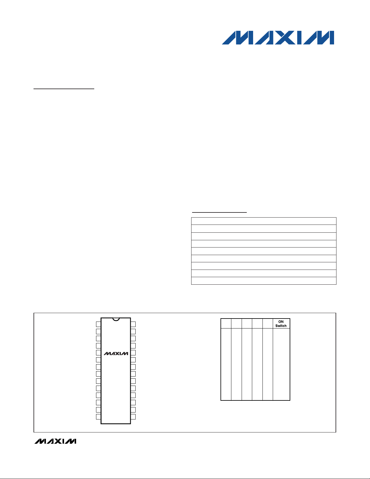
_____________________Pin Configurations/Functional Diagrams/Truth Tables
19-0270; Rev 3; 3/10
PART
MAX306CPI
MAX306CWI 0°C to +70°C
0°C to +70°C
TEMP RANGE PIN-PACKAGE
28 Plastic DIP
28 Wide SO
Ordering Information continued at end of data sheet.
*
Contact factory for dice specifications.
MAX306C/D 0°C to +70°C Dice*
MAX306EPI -40°C to +85°C 28 Plastic DIP
MAX306EWI -40°C to +85°C 28 Wide SO
MAX306EQI -40°C to +85°C 28 PLCC
MAX306MJI -55°C to +125°C 28 CERDIP
For pricing, delivery, and ordering information, please contact Maxim Direct at 1-888-629-4642,
or visit Maxim’s website at www.maxim-ic.com.
MAX306EUI -40°C to +85°C 28 TSSOP
Ordering Information
Sample-and-Hold
Circuits
Test Equipment
Heads-Up Displays
Guidance and Control
Systems
Military Radios
Communications Systems
Battery-Operated Systems
PBX, PABX
Audio Signal Routing
Pin Configurations/Functional Diagrams/Truth Tables
continued at end of data sheet.
TOP VIEW
V+
N.C.
N.C.
NO16
NO15
NO14
NO13
NO12
NO11
NO10
NO9
GND
N.C.
A3
1
2
3
4
5
MAX306
6
7
8
9
10
11
12
13
14
DIP/SO/TSSOP
28
COM
27
V-
26
NO8
25
NO7
24
NO6
23
NO5
22
NO4
21
NO3
NO2
20
NO1
19
EN
18
A0
17
A1
16
A2
15
A3
X
0
0
0
0
0
0
0
0
1
1
1
1
1
1
1
1
LOGIC “0” V
A2 A1 A0 EN
X
X
X
0
0
0
0
0
1
0
1
1
0
1
0
1
1
1
1
0
0
0
0
0
1
0
1
1
0
1
0
1
1
1
1
MAX306
≤ 0.8V, LOGIC “1” = VAH ≥ 2.4V
AL
0
0
1
1
1
0
1
1
1
0
1
1
1
0
1
1
1
0
1
1
1
0
1
1
1
0
1
1
1
0
1
1
1
None
1
2
3
4
5
6
7
8
9
10
11
12
13
14
15
16
MAX306/MAX307
Precision, 16-Channel/Dual 8-Channel,
High-Performance, CMOS Analog Multiplexers
2 _______________________________________________________________________________________
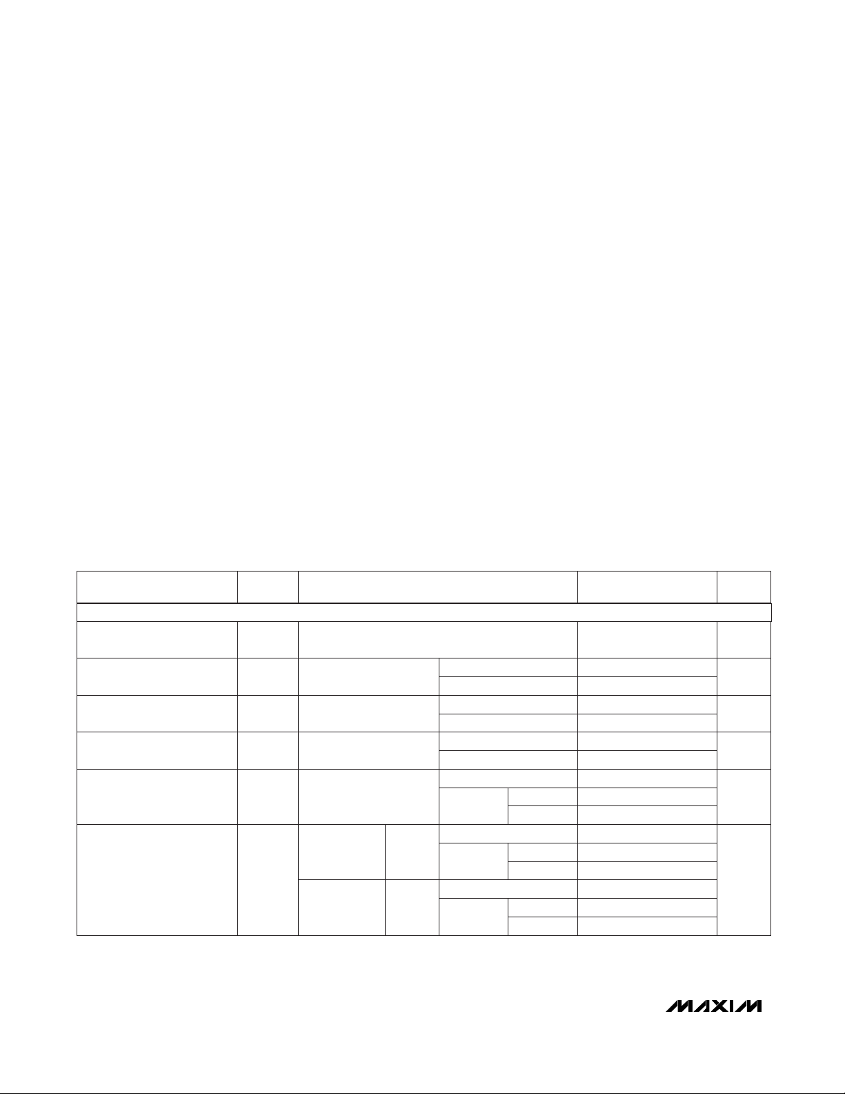
ABSOLUTE MAXIMUM RATINGS
ELECTRICAL CHARACTERISTICS—Dual Supplies
(V+ = +15V, V- = -15V, GND = 0V, VAH= +2.4V, VAL= +0.8V, TA= T
MIN
to T
MAX
, unless otherwise noted.)
Stresses beyond those listed under “Absolute Maximum Ratings” may cause permanent damage to the device. These are stress ratings only, and functional
operation of the device at these or any other conditions beyond those indicated in the operational sections of the specifications is not implied. Exposure to
absolute maximum rating conditions for extended periods may affect device reliability.
(Voltage Referenced to V-)
V+ ..........................................................................-0.3V, +44V
GND.......................................................................-0.3V, +25V
Digital Inputs, NO, COM (Note 1)...........(V- - 2V) to (V+ + 2V) or
30mA (whichever occurs first)
Continuous Current (any terminal) ......................................30mA
Peak Current, NO or COM
(pulsed at 1ms, 10% duty cycle max) ..........................100mA
Continuous Power Dissipation (T
A
= +70°C)
28-Pin Plastic DIP
(derate 9.09mW/°C above +70°C).............................727mW
28-Pin Wide SO (derate 12.50mW/°C above +70°C) ...1000mW
28-Pin PLCC (derate 10.53mW/°C above +70°C)........842mW
28-Pin CERDIP (derate 16.67mW/°C above +70°C) ..1333mW
28-Pin TSSOP (derate 12.8mW/°C above +70°C) ........1025mW
Operating Temperature Ranges
MAX30_C_ _ .......................................................0°C to +70°C
MAX30_E_ _.....................................................-40°C to +85°C
MAX30_MJI....................................................-55°C to +125°C
Storage Temperature Range .............................-65°C to +150°C
Lead Temperature (soldering, 10s) .................................+300°C
Soldering Temperature (reflow)
PDIP lead(Pb)-free .......................................................+260°C
PDIP containing lead(Pb).............................................+240°C
Wide SO lead(Pb)-free.................................................+260°C
Wide SO containing lead(Pb) ......................................+240°C
PLCC lead(Pb)-free......................................................+245°C
PLCC containing lead(Pb) ...........................................+225°C
CERDIP ........................................................................+240°C
TSSOP lead(Pb)-free....................................................+260°C
TSSOP containing lead(Pb) .........................................+240°C
VNO= +10V,
V
COM
= ±10V,
V
EN
= 0V
V
COM
= +10V,
VNO= ±10V,
V
EN
= 0V
INO= -1.0mA,
V
COM
= ±10V
INO= -1.0mA,
V
COM
= ±10V (Note 4)
VNO= ±10V,
V
COM
= +10V,
V
EN
= 0V
CONDITIONS
nA
-20 +20
I
COM(OFF)
COM Off-Leakage Current
(Note 5)
-10 +10
-0.75 +0.02 +0.75
-40 +40
60 100
-20 +20
-0.75 +0.02 +0.75
nA
-5.0 +5.0
I
NO(OFF)
NO Off-Leakage Current
(Note 5)
-2.5 +2.5
Ω
125
R
ON
On-Resistance
1.5 5
Ω
8
ΔR
ON
On-Resistance Matching
Between Channels
UNITS
MIN TYP MAX
(Note 2)
SYMBOLPARAMETER
Note 1: Signals on NO, COM, A0, A1, A2, A3, or EN exceeding V+ or V- are clamped by internal diodes. Limit forward current to
maximum current ratings.
V-15 +15
VNO,
V
COM
Analog Signal Range
INO= -1.0mA,
V
COM
= ±5V or 0V
1.8 7
Ω
10
R
FLAT
On-Resistance Flatness
(Note 3)
TA= +25°C
TA= T
MIN
to T
MAX
TA= +25°C
TA= T
MIN
to T
MAX
TA= +25°C
TA= T
MIN
to T
MAX
-0.5 +0.01 +0.5TA= +25°C
TA= T
MIN
to T
MAX
TA= +25°C
TA= T
MIN
to T
MAX
TA= +25°C
TA= T
MIN
to T
MAX
MAX307
MAX306
C, E
M
C, E
M
C, E
M
SWITCH
MAX306/MAX307
Precision, 16-Channel/Dual 8-Channel,
High-Performance, CMOS Analog Multiplexers
_______________________________________________________________________________________ 3
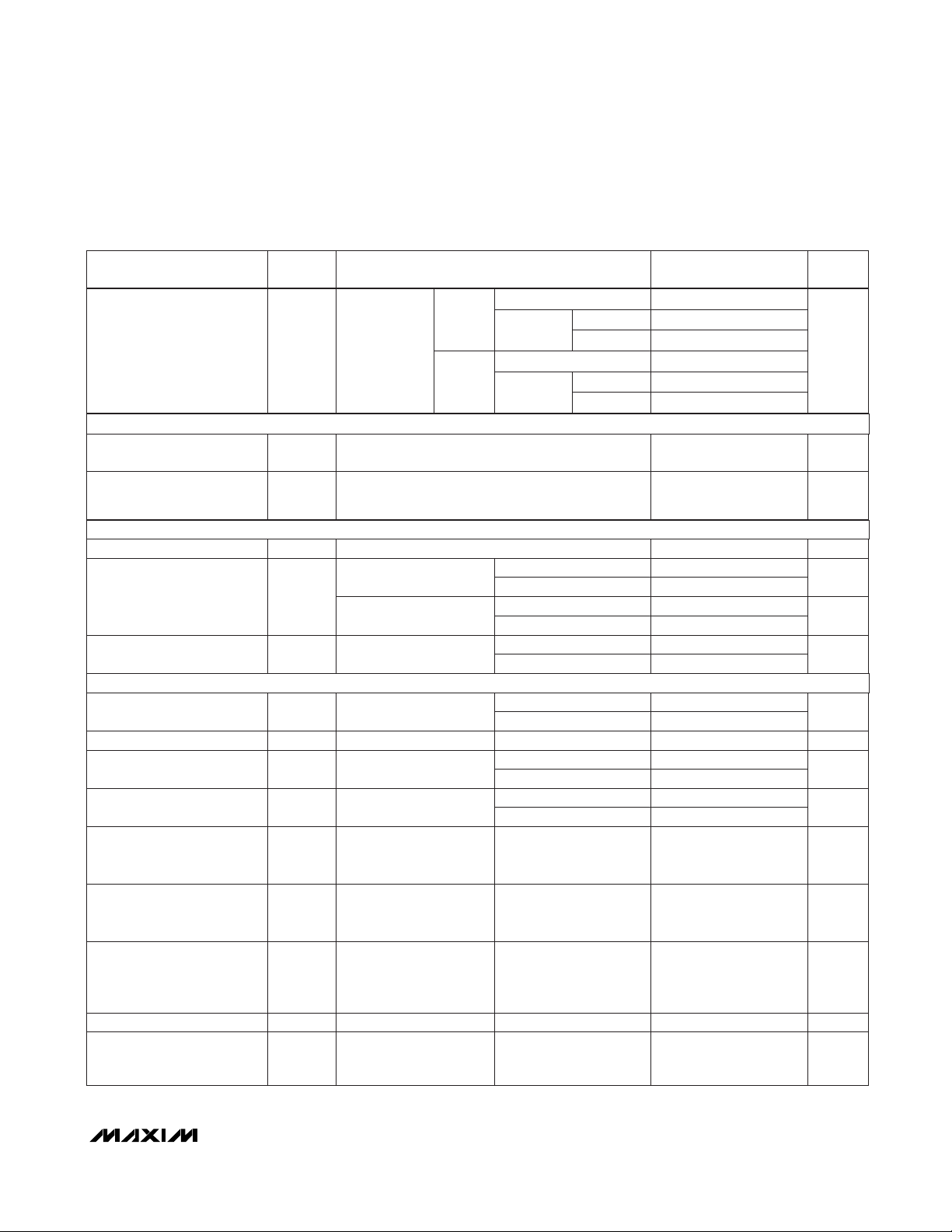
ELECTRICAL CHARACTERISTICS—Dual Supplies (continued)
(V+ = +15V, V- = -15V, GND = 0V, VAH= +2.4V, VAL= +0.8V, TA= T
MIN
to T
MAX
, unless otherwise noted.)
V
COM
= ±10V,
V
NO
= ±10V,
sequence
each switch
on
nA
-25 +25
I
COM(ON)
COM On-Leakage Current
(Note 5)
-12.5 +12.5
-0.75 +0.02 +0.75
-50 +50
-25 +25
-0.75 +0.02 +0.75
Off-Isolation
(Note 6)
dB-69V
ISO
210Q
Charge Injection
(Note 3)
pC
55 150
ns
400
t
ON(EN)
Enable Turn-On Time
130 200
ns10 40t
OPEN
Break-Before-Make Interval
110 300
µA-1.0 +1.0I
AL
Input Current with
Input Voltage Low
µA-1.0 +1.0I
AH
Input Current with
Input Voltage High
µA
-10 +10
I-Negative Supply Current
-1 +1
mA
1
I+Positive Supply Current
0.075 0.5
V±4.5 ±20Power-Supply Range
16 30
µA
75
UNITS
MIN TYP MAX
(Note 2)
SYMBOLPARAMETER
TA= +25°C
TA= T
MIN
to T
MAX
TA= +25°C
TA= T
MIN
to T
MAX
MAX306
MAX307
C, E
M
C, E
M
Crosstalk Between Channels V
CT
-92 dB
Logic Input Capacitance C
IN
8 pF
NO Off-Capacitance C
NO(OFF)
8 pF
TA= +25°C
VEN= 0V or 2.4V,
VA= 0V
TA= +25°C
VA= 2.4V or 15V
TA= +25°C
TA= T
MIN
to T
MAX
TA= T
MIN
to T
MAX
TA= +25°C
TA= +25°C
TA= +25°C
TA= T
MIN
to T
MAX
TA= +25°C
TA= +25°C
TA= +25°C
TA= T
MIN
to T
MAX
CONDITIONS
TA= +25°C
TA= +25°C
TA= +25°C
VEN= 0V,
RL= 1kΩ,
f = 100kHz, Figure 6
CL= 1.0nF,
V
NO
= 0V,
RS= 0Ω, Figure 5
Figure 3
VEN= 2.4V,
V
A(ALL)
= 0V
Figure 4
VEN= 2.4V,
V
A(ALL)
= 0V
VEN= VA= 0V or 5.0V
VEN= 2.4V,
f = 100kHz,
V
GEN
= 1V
P-P
,
R
L
= 1kΩ, Figure 7
f = 1MHz
f = 1MHz,
VEN= VNO= 0V,
Figure 8
ns
400
t
TRANS
Transition Time
TA= T
MIN
to T
MAX
Figure 2
ns
300
t
OFF(EN)
Enable Turn-Off Time
TA= T
MIN
to T
MAX
Figure 3
INPUT
SUPPLY
DYNAMIC
(Note 3)
CL= 1.0nF,
VNO= 0V,
RS= 0Ω
V
INH
= 2.4V,
V
INL
= 0V,
V
NO1
= 5V,
Figure 3
V
INH
= 2.4V,
V
INL
= 0V,
V
NO1
= 5V,
Figure 3
V
NO1
= 8V,
V
NO8
= 0V,
V
IN
= 2.4V,
Figure 1
INO= -1.0mA
V
COM
= 3V or 10V
pC210Q
Charge Injection
(Note 3)
ns80 300t
OFF(EN)
Enable Turn-Off Time
(Note 3)
V012
VNO,
V
COM
Analog Signal Range
ns105 600t
ON(EN)
Enable Turn-On Time
(Note 3)
ns130 450t
TRANS
Transition Time
(Note 3)
Ω120 175R
ON
On-Resistance TA= +25°C
TA= +25°C
TA= +25°C
TA= +25°C
TA= +25°C
SWITCH
DYNAMIC
MAX306/MAX307
Precision, 16-Channel/Dual 8-Channel,
High-Performance, CMOS Analog Multiplexers
4 _______________________________________________________________________________________
CONDITIONS UNITS
MIN TYP MAX
(Note 2)
SYMBOLPARAMETER
ELECTRICAL CHARACTERISTICS—Single Supply
(V+ = +12V, V- = 0V, GND = 0V, VAH= +2.4V, VAL= +0.8V, TA= T
MIN
to T
MAX
, unless otherwise noted.)
Note 2: The algebraic convention where the most negative value is a minimum and the most positive value a maximum is used in
this data sheet.
Note 3: Guaranteed by design.
Note 4: ΔR
ON
= R
ON(MAX)
- R
ON(MIN)
.
On-resistance match between channels and flatness are guaranteed only with specified
voltages. Flatness is defined as the difference between the maximum and minimum value of on-resistance as measured at
the extremes of the specified analog signal range.
Note 5: Leakage parameters are 100% tested at the maximum-rated hot temperature and guaranteed by correlation at +25°C.
Note 6: Off-isolation = 20log V
COM/VNO
, where V
COM
= output and VNO= input to off switch.
COM Off-Capacitance C
COM(OFF)
f = 1MHz,
VEN= 0.8V,
V
COM
= 0V,
Figure 8
COM On-Capacitance C
COM(ON)
f = 1MHz,
VEN= 2.4V,
V
COM
= 0V,
Figure 8
TA= +25°C
TA= +25°C
MAX306
MAX307
MAX306
MAX307
pF
pF
130
65
140
70

MAX306/MAX307
Precision, 16-Channel/Dual 8-Channel,
High-Performance, CMOS Analog Multiplexers
_______________________________________________________________________________________
5
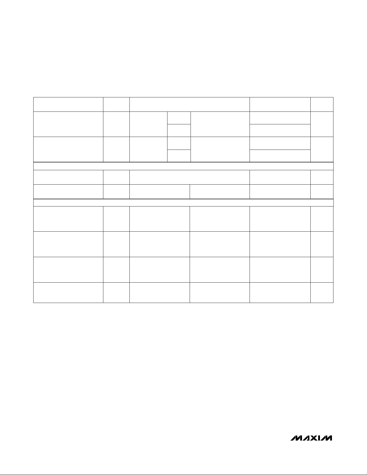
__________________________________________Typical Operating Characteristics
(TA = +25°C, unless otherwise noted.)
ON-RESISTANCE vs. V
160
140
120
100
(Ω)
80
ON
R
60
40
20
0
-20 20-15 15-10 10-5 50
ON-RESISTANCE vs. V
TEMPERATURE (SINGLE SUPPLY)
160
V+ = +15V
140
V- = 0V
120
100
(Ω)
80
ON
R
60
40
20
0
(DUAL SUPPLIES)
±5V
V
(V)
COM
+125°C
+85°C
+25°C
-55°C
V
(V)
COM
COM
COM
±10V
±15V
AND
±20V
MAX306/7 TOC-01
MAX306/7 TOC-04
151050
ON-RESISTANCE vs. V
TEMPERATURE (DUAL SUPPLIES)
120
V+ = +15V
V- = -15V
100
80
(Ω)
60
ON
R
40
20
0
-15 15-10 10-5 50
+125°C
+85°C
+25°C
-55°C
V
COM
(V)
OFF LEAKAGE vs. TEMPERATURE
1000
V+ = +15V
100
V- = -15V
10
1
I
0.1
OFF LEAKAGE (nA)
0.01
0.001
0.0001
-35 -15 65
-55 125
COM (ON)
I
NO (OFF)
45
25
5
TEMPERATURE (°C)
COM
AND
85 105
MAX306/7 TOC-02
(Ω)
R
MAX306/7 TOC-05
ON LEAKAGE (nA)
0.0001
400
360
320
280
240
ON
200
160
120
1000
100
0.01
0.001
80
40
10
0.1
ON-RESISTANCE vs. V
COM
(SINGLE SUPPLY)
5V
10V
15V
20V
15 201050
V
(V)
COM
ON LEAKAGE vs. TEMPERATURE
V+ = +15V
V- = -15V
1
I
COM (ON)
-35 -15 65
-55 125
45
25
5
TEMPERATURE (°C)
85 105
MAX306/7 TOC-03
MAX306/7 TOC-06
CHARGE INJECTION vs. V
30
20
10
0
(pC)
j
Q
-10
-20
-30
-15 15-10 10-5 50
COM
V+ = +15V
V- = -15V
V+ = 12V
V- = 0V
V
(V)
COM
MAX306/7 TOC-07
SUPPLY CURRENT vs. TEMPERATURE
100
I+
10
1
I+, I- (μA)
0.1
I-
0.01
0.001
-35 -15 65
-55 125
V+ = +15V
V- = -15V
= VA = 0V, 4.5V
V
EN
45
25
5
TEMPERATURE (°C)
MAX306/7 TOC-08
85 105

__________Applications Information
Operation with Supply Voltages
Other than ±15V
Using supply voltages other than ±15V will reduce the
analog signal range. The MAX306/MAX307 switches
operate with ±4.5V to ±20V bipolar supplies or with a
+5V to +30V single supply; connect V- to GND when
operating with a single supply. Also, both device types
can operate with unbalanced supplies such as +24V
and -5V. The
Typical Operating Characteristics
graphs
show typical on-resistance with 20V, 15V, 10V, and 5V
supplies. (Switching times increase by a factor of two
or more for operation at 5V.)
Overvoltage Protection
Proper power-supply sequencing is recommended for
all CMOS devices. Do not exceed the absolute maximum ratings because stresses beyond the listed ratings may cause permanent damage to the devices.
Always sequence V+ on first, then V-, followed by either
the logic inputs, NO or COM. If power-supply sequencing is not possible, add two small-signal diodes in
series with supply pins for overvoltage protection
(Figure 1). Adding diodes reduces the analog signal
range to 1V above V+ and 1V below V-, but low switch
resistance and low leakage characteristics are unaffected. Device operation is unchanged, and the difference between V+ and V- should not exceed +44V.
MAX306/MAX307
Precision, 16-Channel/Dual 8-Channel,
High-Performance, CMOS Analog Multiplexers
6 _______________________________________________________________________________________
Output–bidirectionalCOM28
Address InputsA3–A014–17
Enable InputsEN18
Analog Inputs–bidirectionalNO1–NO819–26
Negative Supply Voltage InputV-27
GroundGND12
Analog Inputs–bidirectionalNO16–NO94–11
MAX306
PIN
No Connection. Not internally
connected.
N.C.2, 3, 13
Positive Supply Voltage InputV+1
FUNCTIONNAME
Negative Supply Voltage InputV-27
Output A–bidirectionalCOMA28
GroundGND12
Address InputsA2, A1, A015, 16, 17
Enable InputEN18
Analog Inputs–bidirectionalNO1A–NO8A19–26
Analog Inputs–bidirectionalNO8B–NO1B4–11
No Connection. Not internally
connected.
N.C.3, 13, 14
MAX307
PIN
Output B–bidirectionalCOMB2
Positive Supply Voltage InputV+1
FUNCTIONNAME
_____________________________________________________________Pin Descriptions
Figure 1. Overvoltage Protection Using External Blocking
Diodes
V+
NO
V
g
V-
COM

MAX306/MAX307
Precision, 16-Channel/Dual 8-Channel,
High-Performance, CMOS Analog Multiplexers
_______________________________________________________________________________________ 7
______________________________________________Test Circuits/Timing Diagrams
Figure 2. Transition Time
Figure 3. Enable Switching Time
+15V
V+
NO2-NO15
V-
-15V
V+
NO1A-NO8A
V-
-15V
+15V
NO1
NO16
COM
NO1B
NO8B
COMB
300Ω
300Ω
±10V
+10V
±10V
+10V
35pF
35pF
LOGIC
V
OUT
V
OUT
INPUT
SWITCH
OUTPUT
V
OUT
V
V
+3V
NO1
0V
NO16
50%
0V
90%
t
TRANS
ON
tr < 20ns
tf < 20ns
90%
t
TRANS
50Ω
50Ω
A0
A1
A2
MAX306
A3
EN
GND
+15V
A0
A1
A2
EN
MAX307
GND
EN
A0
A1
A2
A3
50Ω
50Ω
GND
EN
A0
A1
A2
GND
V+
MAX306
+15V
V+
NO2B-NO8B,
MAX307
NO1
NO2-NO16
COM
V-
-15V
NO1B
NO1A-NO8A
COMA
COMB
V-
-15V
1kΩ
1kΩ
-5V
-5V
35pF
35pF
V
OUT
V
OUT
LOGIC
INPUT
SWITCH
OUTPUT
+3V
0V
t
ON(EN)
0V
V
OUT
50%
90%
tr < 20ns
tf < 20ns
10%
t
OFF(EN)

MAX306/MAX307
Precision, 16-Channel/Dual 8-Channel,
High-Performance, CMOS Analog Multiplexers
8 _______________________________________________________________________________________
_________________________________Test Circuits/Timing Diagrams (continued)
Figure 4. Break-Before-Make Interval
Figure 5. Charge Injection
+15V
GND
V+
NO1-NO16
MAX306
COM
V-
-15V
+2.4V
EN
A0
A1
A2
A3
50Ω
+15V
R
S
NO1-NO16
EN
V
S
CHANNEL
SELECT
A0
A1
A2
A3
V+
MAX306
GND
300Ω
V-
-15V
COM
+5V
V
OUT
35pF
V
OUT
CL = 1000nF
LOGIC
INPUT
+3V
LOGIC
INPUT
0V
V
OUT
SWITCH
OUTPUT
0V
+3V
0V
V
OUT
IS THE MEASURED VOLTAGE DUE TO CHARGE TRANSFER
ΔV
OUT
ERROR Q WHEN THE CHANNEL TURNS OFF.
Q = CL = ΔV
OUT
50%
80%
t
OPEN
ONOFF OFF
tr < 20ns
tf < 20ns
ΔV
OUT

MAX306/MAX307
Precision, 16-Channel/Dual 8-Channel,
High-Performance, CMOS Analog Multiplexers
_______________________________________________________________________________________ 9
_________________________________Test Circuits/Timing Diagrams (continued)
Figure 6. Off-Isolation Figure 7. Crosstalk
Figure 8. NO/COM Capacitance
10nF
GND
+15V
V+
MAX306
EN
10nF
COM
V-
-15V
V
V
OUT
IN
10nF
V+
=
R
L
1kΩ
COM
EN
V-
-15V
V
OUT
V
IN
R
V
= 1kΩ
L
OUT
R
S
= 50Ω
R
S
= 50Ω
V
IN
NO1
NO16
A0
A1
A2
A3
GND
OFF-ISOLATION = 20log
+15V
MAX306
10nF
V
OUT
NO1
NO2
NO16
A0
A1
A2
A3
CROSSTALK = 20log
+15V
V+
A3
CHANNEL
SELECT
A2
MAX306
A1
A0
EN
GND
V-
-15V
NO1
NO16
COM
Meter
Impedance
Analyzer
f = 1MHz

MAX306/MAX307
Precision, 16-Channel/Dual 8-Channel,
High-Performance, CMOS Analog Multiplexers
10 ______________________________________________________________________________________
________Pin Configurations/Functional Diagrams/Truth Tables (continued)
TOP VIEW
V+
1
2
COMB
N.C.
3
NO8B
4
5
NO7B
MAX307
6
NO6B
NO5B
7
NO4B
8
NO3B
9
10
NO2B
NO1B
GND
N.C.
N.C.
11
12
13
14
COMA
28
27
V-
26
NO8A
25
NO7A
NO6A
24
NO5A
23
NO4A
22
NO3A
21
NO2A
20
NO1A
19
EN
18
A0
17
A1
16
A2
15
A2 A1 A0 EN
X
0
0
0
0
1
1
1
1
LOGIC “0” V
AL
X
X
0
0
0
0
1
1
0
1
1
0
0
0
1
1
0
1
1
MAX307
≤ 0.8V, LOGIC “1” = VAH ≥ 2.4V
None
1
1
1
2
1
3
1
4
1
5
1
6
1
7
1
8
TOP VIEW
NO15
NO14
NO13
NO12
NO11
10
NO10
NO9
11
N.C. = NO INTERNAL CONNECTION
NO16
5
6
7
8
9
12
GND
DIP/SO
N.C.
N.C.V+COMV-NO8
1234
MAX306
14 15
13
A3A2A1
N.C.
PLCC
V+ V- GND
2627
28
25
NO7
24
NO6
NO5
23
22
NO4
N03
21
20
N02
19
N01
17
16
18
A0
EN
NO1
NO2
NO3
NO4
NO5
NO6
NO7
NO8
NO9
NO10
NO11
NO12
NO13
NO14
NO15
NO16
COM
CMOS DECODERS/DRIVERS
A0 A1 A2 A3 EN
MAX306 16-CHANNEL SINGLE-ENDED MULTIPLEXER

MAX306/MAX307
Precision, 16-Channel/Dual 8-Channel,
High-Performance, CMOS Analog Multiplexers
______________________________________________________________________________________ 11
________Pin Configurations/Functional Diagrams/Truth Tables (continued)
_Ordering Information (continued)
* Contact factory for dice specifications.
28 TSSOP-40°C to +85°CMAX307EUI
28 PLCC-40°C to +85°CMAX307EQI
28 Wide SO-40°C to +85°CMAX307EWI
28 Plastic DIP-40°C to +85°CMAX307EPI
Dice*0°C to +70°CMAX307C/D
28 Wide SO
28 Plastic DIP
PIN-PACKAGETEMP RANGE
0°C to +70°C
0°C to +70°CMAX307CWI
MAX307CPI
PART
28 CERDIP-55°C to +125°CMAX307MJI
PACKAGE TYPE PACKAGE CODE DOCUMENT NO.
28 PDIP P28+3
21-0044
28 Wide SO W28+6
21-0042
28 PLCC Q28+4
21-0049
28 CDIP J28-2
21-0046
28 TSSOP U28+2
21-0066
Package Information
For the latest package outline information and land patterns,
go to www.maxim-ic.com/packages
. Note that a “+”, “#”, or
“-” in the package code indicates RoHS status only. Package
drawings may show a different suffix character, but the drawing
pertains to the package regardless of RoHS status.
TOP VIEW
NO7B
NO6B
NO5B
NO4B
NO3B
NO2B
NO1B
NO8B
N.C.
COMBV+COMAV-NO8A
1234
5
6
7
12
GND
MAX307
14 151617
13
N.C.
N.C.
A2A1A0
8
9
10
11
PLCC
N.C. = NO INTERNAL CONNECTION
V+ V-
NO1A
2627
28
25
NO7A
24
NO6A
NO5A
23
22
NO4A
N03A
21
20
N02A
19
N01A
18
EN
NO2A
NO3A
NO4A
NO5A
NO6A
NO7A
NO8A
NO1B
NO2B
NO3B
NO4B
NO5B
NO6B
NO7B
NO8B
CMOS DECODERS/DRIVERS
A0 A1 A2
MAX307 8-CHANNEL DIFFERENTIAL MULTIPLEXER
GND
COMA
COMB
EN

MAX306/MAX307
Precision, 16-Channel/Dual 8-Channel,
High-Performance, CMOS Analog Multiplexers
12 ______________________________________________________________________________________
__________________________________________________________Chip Topographies
TRANSISTOR COUNT: 269
SUBSTRATE IS INTERNALLY CONNECTED TO V+
TRANSISTOR COUNT: 269
SUBSTRATE IS INTERNALLY CONNECTED TO V+
MAX306
MAX307
N.C. = NO INTERNAL CONNECTION
EN
A0 A1 A2 A3 N.C.
NO1
NO2
NO3
N04
NO5
NO6
NO7
NO8
0.184"
(4.67mm)
GND
NO9
NO10
NO11
NO12
N013
NO14
NO15
NO16
N.C.
NO1A
NO2A
NO3A
N04A
NO5A
NO6A
NO7A
NO8A
EN
A0 A1 A2 N.C. N.C.
0.184"
(4.67mm)
GND
NO1B
NO2B
NO3B
NO4B
N05B
NO6B
NO7B
NO8B
COMB
V- COM V+
0.078"
(1.98mm)
V- COMA V+
0.078"
(1.98mm)

MAX306/MAX307
Precision, 16-Channel/Dual 8-Channel,
High-Performance, CMOS Analog Multiplexers
Maxim cannot assume responsibility for use of any circuitry other than circuitry entirely embodied in a Maxim product. No circuit patent licenses are
implied. Maxim reserves the right to change the circuitry and specifications without notice at any time.
Maxim Integrated Products, 120 San Gabriel Drive, Sunnyvale, CA 94086 408-737-7600 ____________________
13
© 2010 Maxim Integrated Products Maxim is a registered trademark of Maxim Integrated Products, Inc.
Revision History
REVISION
NUMBER
3 3/10
REVISION
DATE
DESCRIPTION
Changed the s ingle-supply operating vo ltage minimum from +4.5V to +5V in the
General De scription, Features, and Applications Information sections.
Added the soldering temperatures for all packages to the Absolute Maximum Ratings
section.
PAGES
CHANGED
1, 6
2
 Loading...