

Page 1
For pricing, delivery, and ordering information, please contact Maxim Direct at 1-888-629-4642,
or visit Maxim's website at www.maxim-ic.com.
MAX3060E/MAX3061E/MAX3062E
±15kV ESD-Protected, Fail-Safe, 20Mbps, Slew-Rate-
Limited RS-485/RS-422 Transceivers in a SOT
________________________________________________________________ Maxim Integrated Products 1
General Description
The MAX3060E/MAX3061E/MAX3062E high-speed
transceivers for RS-485/RS-422 communication contain
one driver and one receiver. These devices feature failsafe circuitry, which guarantees a logic-high receiver
output when the receiver inputs are open or shorted.
This means that the receiver output is a logic high if all
transmitters on a terminated bus are disabled (high
impedance). These devices also feature hot-swap circuitry that eliminates data glitches during hot insertion.
The MAX3060E features slew-rate-limited drivers that
minimize EMI and reduce reflections caused by
improperly terminated cables, allowing error-free data
transmission up to 115kbps. The MAX3061E, also slewrate limited, transmits up to 500kbps. The MAX3062E
driver is not slew-rate limited, allowing transmit speeds
up to 20Mbps. All transmitter outputs are protected to
±15kV using the Human Body Model.
These transceivers typically draw 910µA of supply
current when unloaded, or 790µA when fully loaded
with the drivers disabled.
All devices have a 1/8-unit-load receiver input impedance that allows up to 256 transceivers on the bus. These
devices are intended for half-duplex communication.
Applications
RS-422/RS-485 Communications
Level Translators
Transceivers for EMI-Sensitive Applications
Industrial-Control Local-Area Networks
Features
♦ True Fail-Safe Receiver While Maintaining
EIA/TIA-485 Compatibility
♦ Enhanced Slew-Rate Limiting Facilitates
Error- Free Data Transmission (MAX3060E and
MAX3061E)
♦ 1nA Low-Current Shutdown Mode
♦ Hot-Swappable for Telecom Applications
♦ ESD Protection: ±15kV Human Body Model
♦ Allow Up to 256 Transceivers on the Bus
♦ Space-Saving 8-Pin SOT23 Package
19-2536; Rev 1; 7/07
Ordering Information
PART
PIN-
TOP
MARK
MAX3060EEKA-T
AAKI
MAX3060EEKA#T
AEPA*
MAX3061EEKA-T
AAKJ
MAX3061EEKA#T
AEPB*
MAX3062EEKA-T
AAKK
MAX3062EEKA#T
AEPC*
Selector Guide
PART
DATA
RATE
(Mbps)
SLEW-
RATE
TRANSCEIVERS
ON BUS
MAX3060E
0.115 Yes 256
MAX3061E
0.5 Yes 256
MAX3062E
20 No 256
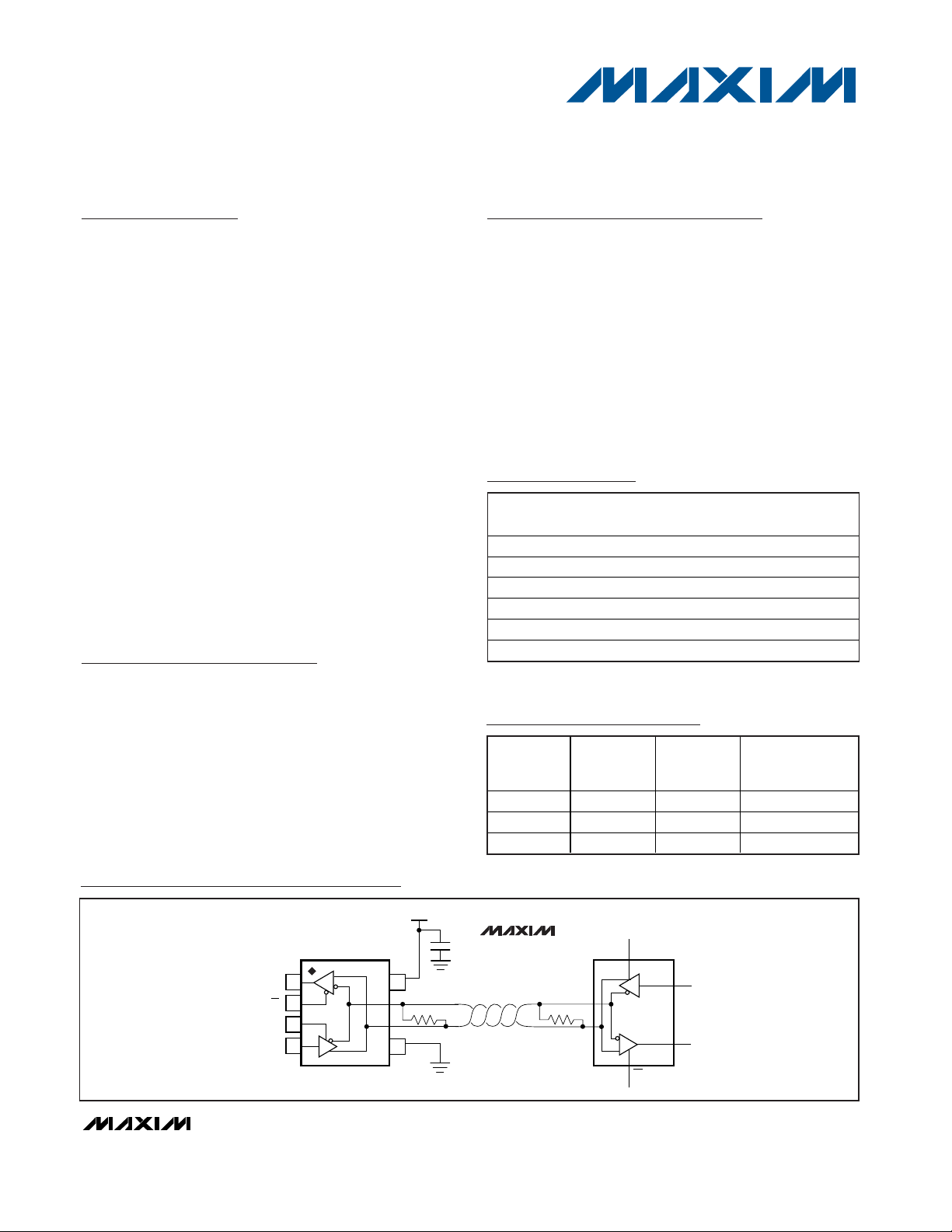
Typical Operating Circuit/Pin Configuration
*Indicates an RoHS-compliant part
T = Tape and Reel
TEMP RANGE
-40°C to +85°C 8 SOT23-8
-40°C to +85°C 8 SOT23-8
-40°C to +85°C 8 SOT23-8
-40°C to +85°C 8 SOT23-8
-40°C to +85°C 8 SOT23-8
-40°C to +85°C 8 SOT23-8
PACKAGE
LIMITED
TOP VIEW
1
RO
2
RE
3
DE
4
DI
R
D
+5V
0.1μF
MAX3060E
MAX3061E
8
V
CC
B
7
Rt
6
A
5
GND
MAX3062E
B
Rt
A
DE
D
R
DI
RO
RE
Page 2
MAX3060E/MAX3061E/MAX3062E
±15kV ESD-Protected, Fail-Safe, 20Mbps, Slew-RateLimited RS-485/RS-422 Transceivers in a SOT
2 _______________________________________________________________________________________
ABSOLUTE MAXIMUM RATINGS
DC ELECTRICAL CHARACTERISTICS
(VCC= +5V ±5%, TA= T
MIN
to T
MAX
, unless otherwise noted. Typical values are at VCC= +5V and TA= +25°C.) (Notes 1, 2)
Stresses beyond those listed under “Absolute Maximum Ratings” may cause permanent damage to the device. These are stress ratings only, and functional
operation of the device at these or any other conditions beyond those indicated in the operational sections of the specifications is not implied. Exposure to
absolute maximum rating conditions for extended periods may affect device reliability.
All Voltages with Respect to GND
Supply Voltage (V
CC
) ............................................................+7V
Input Voltage (
RE, DE, DI)..........................-0.3V to (VCC+ 0.3V)
Driver Output/Receiver Input Voltage (A, B) .......-7.5V to +12.5V
Receiver Output Voltage (RO)....................-0.3V to (V
CC
+ 0.3V)
Continuous Power Dissipation (T
A
= +70°C)
8-Pin SOT23 (derate 8.9mW/°C above +70°C)............714mW
Operating Temperature Range
MAX306_EE_ _ ................................................-40°C to +85°C
Storage Temperature Range .............................-65°C to +150°C
Junction Temperature......................................................+150°C
Lead Temperature (soldering, 10s) .................................+300°C
PARAMETER
SYMBOL
CONDITIONS
MIN
TYP
MAX
UNITS
DRIVER
Differential Driver Output
(No Load)
V
OD1
VCC = 5V 5 V
Figure 1, R = 50Ω (RS-422) 2.0
Differential Driver Output V
OD2
Figure 1, R = 27Ω (RS-485) 1.5
V
Change in Magnitude of
Differential Output Voltage
ΔV
OD
Figure 1, R = 50Ω or R = 27Ω (Note 3) 0.2 V
Driver Common-Mode Output
Voltage
V
OC
Figure 1, R = 50Ω or R = 27Ω 3V
Change in Magnitude of
Common-Mode Voltage
ΔV
OC
Figure 1, R = 50Ω or R = 27Ω (Note 3) 0.2 V
Input High Voltage V
IH
DE, DI, RE 2.0 V
Input Low Voltage V
IL
DE, DI, RE 0.8 V
DI Input Hysteresis V
HYS
mV
Input Current I
IN1
DE, DI, RE ±1 µA
Hot-Swap Driver Input Current
DE, RE (Note 4)
µA
VIN = +12V
Input Current (A and B) I
IN2
DE = GND,
V
CC
= GND or 5.25V
V
IN
= -7V
µA
Driver Short-Circuit Output
Current
V
OD1
-7V ≤ V
OUT
≤ +12V, TA = +25°C (Note 5)
mA
IEC 1000-4-2 Air-Gap Discharge ±7
IEC 1000-4-2 Contact Discharge ±7ESD Protection for A, B
Human Body Model
kV
I
HOTSWAP
100
±200
125
-100
±15 ±250
±15
Page 3
MAX3060E/MAX3061E/MAX3062E
±15kV ESD-Protected, Fail-Safe, 20Mbps, Slew-Rate-
Limited RS-485/RS-422 Transceivers in a SOT
_______________________________________________________________________________________ 3
DC ELECTRICAL CHARACTERISTICS (continued)
(VCC= +5V ±5%, TA= T
MIN
to T
MAX
, unless otherwise noted. Typical values are at VCC= +5V and TA= +25°C.) (Notes 1, 2)
PARAMETER
CONDITIONS
UNITS
RECEIVER
Receiver Differential Threshold
Voltage
V
TH
-7V ≤ VCM ≤ +12V
-50 mV
Receiver Input Hysteresis ΔV
TH
25 mV
Receiver Output High Voltage V
OH
IO = -4mA, VID = -50mV
V
Receiver Output Low Voltage V
OL
IO = 4mA, VID = -200mV 0.4 V
Three-State Output Current at
Receiver
I
OZR
0V ≤ VO ≤ V
CC
±1 µA
Receiver Input Resistance R
IN
-7V ≤ VCM ≤ +12V 96 kΩ
Receiver Output Short-Circuit
Current
I
OSR
0V ≤ V
RO
≤ V
CC
±8
mA
SUPPLY CURRENT
Supply Current I
CC
No load,
DI = GND or V
CC
µA
Supply Current in Shutdown
Mode
I
SHDN
DE = GND, RE = V
CC
1µA
SYMBOL
MIN TYP MAX
-200 -125
VCC - 1.5
0.01
±80
DE = RE = GND 790 1400
DE = RE = V
CC
910 1500
0.001
Page 4
MAX3060E/MAX3061E/MAX3062E
±15kV ESD-Protected, Fail-Safe, 20Mbps, Slew-RateLimited RS-485/RS-422 Transceivers in a SOT
4 _______________________________________________________________________________________
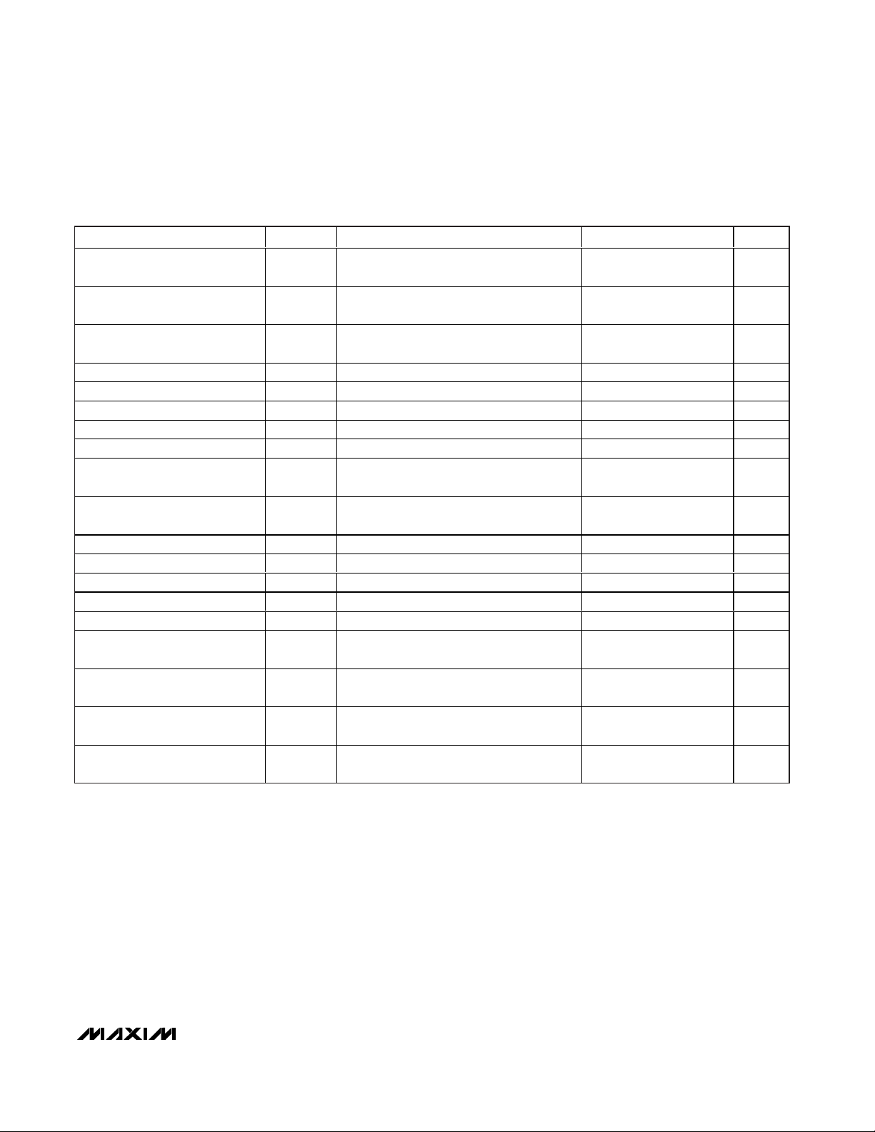
SWITCHING CHARACTERISTICS—MAX3060E
(VCC= +5V ±5%, TA= T
MIN
to T
MAX
, unless otherwise noted. Typical values are at VCC= +5V and TA= +25°C.) (Notes 1, 2)
PARAMETER
CONDITIONS
UNITS
Driver Input to Output
Figures 3 and 5, R
DIFF
= 54Ω,
C
DIFF
= 50pF
1.0 1.7 2.4 µs
Driver Output Skew
(t
DPLH
- t
DPHL
)
t
DSKEW
Figures 3 and 5, R
DIFF
= 54Ω,
C
DIFF
= 50pF
-7
ns
Driver Rise or Fall Time
Figures 3 and 5, R
DIFF
= 54Ω,
C
DIFF
= 50pF
1.3
2.5 µs
Maximum Data Rate f
MAX
kbps
Driver Enable to Output High t
DZH
Figures 4 and 6, CL = 100pF, S2 closed 0.6 1.5 µs
Driver Enable to Output Low t
DZL
Figures 4 and 6, CL = 100pF, S1 closed 0.5 1.5 µs
Driver Disable Time from Low t
DLZ
Figures 4 and 6, CL = 15pF, S1 closed 60
ns
Driver Disable Time from High t
DHZ
Figures 4 and 6, CL = 15pF, S2 closed 85
ns
Receiver Input to Output
t
RPLH
,
t
RPHL
Figures 7 and 9; | VID | ≥ 2.0V;
rise and fall time of V
ID
≤ 4ns, CL = 15pF
47 80 ns
Differential Receiver Skew
(t
RPLH
- t
RPHL
)
t
RSKD
Figures 7 and 9; | VID | ≥ 2.0V;
rise and fall time of V
ID
≤ 4ns, CL = 15pF
-10 -3
ns
Receiver Enable to Output Low t
RZL
Figures 2 and 8, CL = 15pF, S1 closed 50 ns
Receiver Enable to Output High t
RZH
Figures 2 and 8, CL = 15pF, S2 closed 50 ns
Receiver Disable Time from Low
t
RLZ
Figures 2 and 8, CL = 15pF, S1 closed 50 ns
Receiver Disable Time from High
t
RHZ
Figures 2 and 8, CL = 15pF, S2 closed 50 ns
Time to Shutdown t
SHDN
(Note 6) 50
ns
Driver Enable from Shutdown to
Output High
)
Figures 4 and 6, CL = 100pF, S2 closed 2 µs
Driver Enable from Shutdown to
Output Low
)
Figures 4 and 6, CL = 100pF, S1 closed 2 µs
Receiver Enable from Shutdown
to Output High
)
Figures 2 and 8, CL = 15pF, S2 closed 1.5 µs
Receiver Enable from Shutdown
to Output Low
)
Figures 2 and 8, CL = 15pF, S1 closed 1.5 µs
SYMBOL
t
, t
DPLH
DPHL
MIN TYP MAX
tDR, t
DF
t
DZH(SHDN
t
DZL(SHDN
t
RZH(SHDN
t
RZL(SHDN
-200
1.85
115
180 600
+200
200
200
+10
Page 5
MAX3060E/MAX3061E/MAX3062E
±15kV ESD-Protected, Fail-Safe, 20Mbps, Slew-Rate-
Limited RS-485/RS-422 Transceivers in a SOT
_______________________________________________________________________________________ 5
SWITCHING CHARACTERISTICS—MAX3061E
(VCC= +5V ±5%, TA= T
MIN
to T
MAX
, unless otherwise noted. Typical values are at VCC= +5V and TA= +25°C.) (Notes 1, 2)
PARAMETER
CONDITIONS
UNITS
Driver Input to Output
t
DPLH
,
t
DPHL
Figures 3 and 5, R
DIFF
= 54Ω,
C
DIFF
= 50pF
800 ns
Driver Output Skew
(t
DPLH
- t
DPHL
)
t
DSKEW
Figures 3 and 5, R
DIFF
= 54Ω,
C
DIFF
= 50pF
-4
ns
Driver Rise or Fall Time
Figures 3 and 5, R
DIFF
= 54Ω,
C
DIFF
= 50pF
750 ns
Maximum Data Rate f
MAX
kbps
Driver Enable to Output High t
DZH
Figures 4 and 6, CL = 100pF, S2 closed
ns
Driver Enable to Output Low t
DZL
Figures 4 and 6, CL = 100pF, S1 closed
ns
Driver Disable Time from Low t
DLZ
Figures 4 and 6, CL = 15pF, S1 closed 60 200 ns
Driver Disable Time from High t
DHZ
Figures 4 and 6, CL = 15pF, S2 closed 80 200 ns
Receiver Input to Output
t
RPLH
,
t
RPHL
Figures 7 and 9; | VID | ≥ 2.0V;
rise and fall time of V
ID
≤ 4ns, CL = 15pF
47 80 ns
Differential Receiver Skew
(t
RPLH
- t
RPHL
)
t
RSKD
Figures 7 and 9; | VID | ≥ 2.0V;
rise and fall time of V
ID
≤ 4ns, CL = 15pF
-10 -3
ns
Receiver Enable to Output Low t
RZL
Figures 2 and 8, CL = 15pF, S1 closed 50 ns
Receiver Enable to Output High t
RZH
Figures 2 and 8, CL = 15pF, S2 closed 50 ns
Receiver Disable Time from Low
t
RLZ
Figures 2 and 8, CL = 15pF, S1 closed 50 ns
Receiver Disable Time from High
t
RHZ
Figures 2 and 8, CL = 15pF, S2 closed 50 ns
Time to Shutdown t
SHDN
(Note 6) 50
600 ns
Driver Enable from Shutdown to
Output High
Figures 4 and 6, CL = 100pF, S2 closed 1.5 µs
Driver Enable from Shutdown to
Output Low
)
Figures 4 and 6, CL = 100pF, S1 closed 1.5 µs
Receiver Enable from Shutdown
to Output High
)
Figures 2 and 8, CL = 15pF, S2 closed 1.5 µs
Receiver Enable from Shutdown
to Output Low
)
Figures 2 and 8, CL = 15pF, S1 closed 1.5 µs
SYMBOL
MIN TYP MAX
250 470
-100
tDR, t
DF
200 530
500
330 1000
200 1000
t
DZH(SHDN
t
DZL(SHDN
t
RZH(SHDN
t
RZL(SHDN
180
+100
+10
Page 6
MAX3060E/MAX3061E/MAX3062E
±15kV ESD-Protected, Fail-Safe, 20Mbps, Slew-RateLimited RS-485/RS-422 Transceivers in a SOT
6 _______________________________________________________________________________________
SWITCHING CHARACTERISTICS—MAX3062E
(VCC= +5V ±5%, TA= T
MIN
to T
MAX
, unless otherwise noted. Typical values are at VCC= +5V and TA= +25°C.) (Notes 1, 2)
Note 1: Overtemperature limits are guaranteed by design and are not production tested. Devices are tested at T
A
= +25°C.
Note 2: All currents into the device are positive; all currents out of the device are negative. All voltages are referred to device
ground, unless otherwise noted.
Note 3: ΔV
OD
and ΔVOCare the changes in VODand VOC, respectively, when the DI input changes state.
Note 4: This input current level is for the hot-swap enable (DE, RE) inputs and is present until the first transition only. After the first
transition, the input reverts to a standard high-impedance CMOS input with input current I
IN1
. For the first 10µs, the input
current can be as high as 1mA. During this period the input is disabled.
Note 5: Maximum current level applies to peak current just prior to foldback-current limiting; minimum current level applies during
current limiting.
Note 6: The device is put into shutdown by bringing RE high and DE low. If the enable inputs are in this state for less than 50ns, the
device is guaranteed not to enter shutdown. If the enable inputs are in this state for at least 600ns, the device is guaranteed
to have entered shutdown.
PARAMETER
CONDITIONS
UNITS
Driver Input to Output
t
DPLH
,
t
DPHL
Figures 3 and 5, R
DIFF
= 54Ω,
C
DIFF
= 50pF
20 30 ns
Driver Output Skew
(t
DPLH
- t
DPHL
)
t
DSKEW
Figures 3 and 5, R
DIFF
= 54Ω,
C
DIFF
= 50pF
-10 +1
ns
Driver Rise or Fall Time
Figures 3 and 5, R
DIFF
= 54Ω,
C
DIFF
= 50pF
815ns
Maximum Data Rate f
MAX
20
Mbps
Driver Enable to Output High t
DZH
Figures 4 and 6, CL = 100pF, S2 closed
500 ns
Driver Enable to Output Low t
DZL
Figures 4 and 6, CL = 100pF, S1 closed
500 ns
Driver Disable Time from Low t
DLZ
Figures 4 and 6, CL = 15pF, S1 closed
200 ns
Driver Disable Time from High t
DHZ
Figures 4 and 6, CL = 15pF, S2 closed
200 ns
Receiver Input to Output
t
RPLH
,
t
RPHL
Figures 7 and 9; | VID | ≥ 2.0V;
rise and fall time of V
ID
≤ 4ns, CL = 15pF
45 80 ns
Differential Receiver Skew
(t
RPLH
- t
RPHL
)
t
RSKD
Figures 7 and 9; | VID | ≥ 2.0V;
rise and fall time of V
ID
≤ 4ns, CL = 15pF
-10 -4
ns
Receiver Enable to Output Low t
RZL
Figures 2 and 8, CL = 15pF, S1 closed 50 ns
Receiver Enable to Output High t
RZH
Figures 2 and 8, CL = 15pF, S2 closed 50 ns
Receiver Disable Time from Low
t
RLZ
Figures 2 and 8, CL = 15pF, S1 closed 50 ns
Recei ver D i sab l e Ti m e fr om H i g ht
RHZ
Figures 2 and 8, CL = 15pF, S2 closed 50 ns
Time to Shutdown t
SHDN
(Note 6) 50
600 ns
Driver Enable from Shutdown to
Output High
)
Figures 4 and 6, CL = 100pF, S2 closed 100 ns
Driver Enable from Shutdown to
Output Low
)
Figures 4 and 6, CL = 100pF, S1 closed 100 ns
Receiver Enable from Shutdown
to Output High
)
Figures 2 and 8, CL = 15pF, S2 closed 1.5 µs
Receiver Enable from Shutdown
to Output Low
)
Figures 2 and 8, CL = 15pF, S1 closed 1.5 µs
SYMBOL
tDR, t
DF
MIN TYP MAX
+10
250
250
100
100
+10
t
DZH(SHDN
t
DZL(SHDN
t
RZH(SHDN
t
RZL(SHDN
180
Page 7

MAX3060E/MAX3061E/MAX3062E
±15kV ESD-Protected, Fail-Safe, 20Mbps, Slew-Rate-
Limited RS-485/RS-422 Transceivers in a SOT
R
R
A
B
V
OD2
V
OC
Figure 1. Driver DC Test Load
RECEIVER
OUTPUT
TEST POINT
1kΩ
1kΩ
S1
S2
V
CC
C
L
15pF
Figure 2. Receiver Enable/Disable Timing Test Load
DI
DE
5V
A
B
C
DIFF
R
DIFF
V
OD2
Figure 3. Driver Timing Test Circuit Figure 4. Driver Enable/Disable Timing Test Load
DI
5V
0
B
A
V
O
0
-V
O
1.5V
t
DPLH
10%
t
DR
90%
90%
t
DPHL
1.5V
10%
t
DF
V
DIFF
= V (A) - V (B)
V
DIFF
t
DSKEW = | tDPLH
- t
DPHL
|
Figure 5. Driver Propagation Delays Figure 6. Driver Enable and Disable Times
_______________________________________________________________________________________ 7
OUTPUT
500Ω
UNDER TEST
C
L
V
S1
CC
S2
5V
DE
A, B
V
A, B
1.5V 1.5V
0
t
, t
DZL(SHDN)
DZL
2.3V
OL
0
OUTPUT NORMALLY LOW
OUTPUT NORMALLY HIGH
2.3V
t
, t
DZH(SHDN)
DZH
t
DLZ
V
+ 0.5V
OL
V
- 0.5V
OH
t
DHZ
Page 8
MAX3060E/MAX3061E/MAX3062E
±15kV ESD-Protected, Fail-Safe, 20Mbps, Slew-RateLimited RS-485/RS-422 Transceivers in a SOT
8 _______________________________________________________________________________________
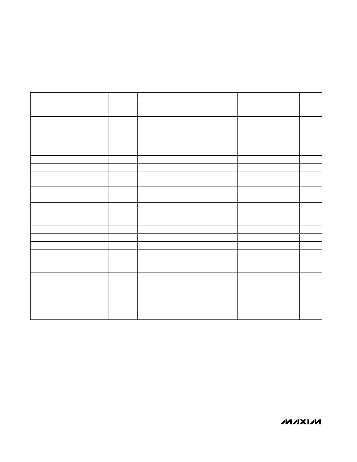
NO-LOAD SUPPLY CURRENT
vs. TEMPERATURE
MAX3060E toc01
TEMPERATURE (°C)
NO-LOAD SUPPLY CURRENT (μA)
603510-15
700
750
800
850
900
950
650
-40 85
DE = RE = V
CC
DE = RE = GND
RECEIVER OUTPUT CURRENT
vs. RECEIVER OUTPUT LOW VOLTAGE
MAX3060E toc02
OUTPUT LOW VOLTAGE (V)
OUTPUT CURRENT (mA)
4321
10
20
30
40
50
60
0
05
RECEIVER OUTPUT CURRENT
vs. RECEIVER OUTPUT HIGH VOLTAGE
MAX3060E toc03
OUTPUT HIGH VOLTAGE (V)
OUTPUT CURRENT (mA)
4321
2
4
6
8
10
12
14
16
18
20
0
05
Typical Operating Characteristics
(VCC= +5V, TA = +25°C, unless otherwise noted.)
V
OH
V
OL
A
B
1V
-1V
1.5V 1.5V
OUTPUT
INPUT
RO
t
RPLH
t
RPHL
Figure 7. Receiver Propagation Delays Figure 8. Receiver Enable and Disable Times
R
B
RECEIVER
OUTPUT
ATE
A
V
ID
R
Figure 9. Receiver Propagation Delay Test Circuit
5V
RE
V
RO
RO
1.5V 1.5V
0
t
, t
RZL(SHDN)
CC
0
1.5V
1.5V
RZL
OUTPUT NORMALLY LOW
OUTPUT NORMALLY HIGH
t
, t
RZH(SHDN)
RZH
t
RLZ
VOL + 0.5V
V
- 0.5V
OH
t
RHZ
Page 9

MAX3060E/MAX3061E/MAX3062E
±15kV ESD-Protected, Fail-Safe, 20Mbps, Slew-Rate-
Limited RS-485/RS-422 Transceivers in a SOT
_______________________________________________________________________________________ 9
MAX3060E/MAX3061E/MAX3062E
Typical Operating Characteristics (continued)
(VCC= +5V, TA = +25°C, unless otherwise noted.)
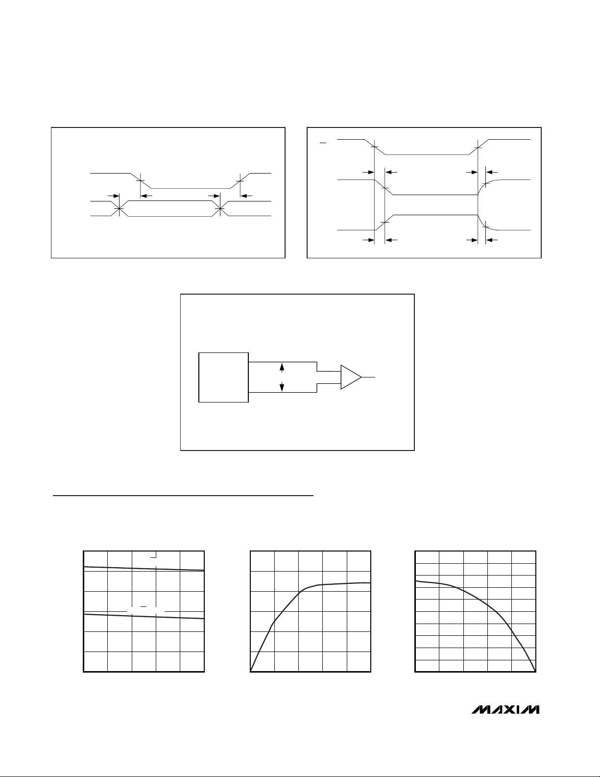
SHUTDOWN CURRENT
vs. TEMPERATURE
MAX3060E toc04
TEMPERATURE (°C)
SHUTDOWN CURRENT (nA)
603510-15
0.5
1.0
1.5
2.0
2.5
3.0
3.5
4.0
4.5
5.0
0
-40 85
RECEIVER OUTPUT LOW VOLTAGE
vs. TEMPERATURE
MAX3060E toc05
TEMPERATURE (°C)
OUTPUT LOW VOLTAGE (V)
6035-15 10
0.15
0.20
0.25
0.30
0.35
0.40
0.45
0.50
0.10
-40 85
IRO = 8mA
RECEIVER OUTPUT HIGH VOLTAGE
vs. TEMPERATURE
MAX3060E toc06
TEMPERATURE (°C)
OUTPUT HIGH VOLTAGE (V)
603510-15
3.4
3.6
3.8
4.0
4.2
3.2
-40 85
IRO = -8mA
RECEIVER PROPAGATION DELAY
(MAX3060E/MAX3061E) vs. TEMPERATURE
MAX3060E toc07
TEMPERATURE (°C)
PROPAGATION DEALY (ns)
603510-15
25
30
35
40
45
50
55
60
65
70
20
-40 85
CL = 15pF
DRIVER PROPAGATION DELAY
(MAX3060E) vs. TEMPERATURE
MAX3060E toc09
TEMPERATURE (°C)
PROPAGATION DEALY (μs)
603510-15
1.62
1.64
1.66
1.68
1.70
1.72
1.74
1.76
1.78
1.80
1.60
-40 85
Rt = 54
Ω
DRIVER PROPAGATION DELAY
(MAX3061E) vs. TEMPERATURE
MAX3060E toc10
TEMPERATURE (°C)
PROPAGATION DELAY (ns)
603510-15
420
440
460
480
500
520
540
400
-40 85
Rt = 54
Ω
DRIVER PROPAGATION DELAY
(MAX3062E) vs. TEMPERATURE
MAX3060E toc11
TEMPERATURE (°C)
PROPAGATION DELAY (ns)
603510-15
5
10
15
20
25
30
0
-40 85
Rt = 54
Ω
DRIVER DIFFERENTIAL OUTPUT VOLTAGE
vs. TEMPERATURE
MAX3060E toc12
TEMPERATURE (°C)
OUTPUT VOLTAGE (V)
603510-15
2.2
2.4
2.6
2.8
3.0
3.2
3.4
2.0
-40 85
Rt = 54
Ω
RECEIVER PROPAGATION DELAY
(MAX3062E) vs. TEMPERATURE
MAX3060E toc08
TEMPERATURE (°C)
PROPAGATION DEALY (ns)
603510-15
25
30
35
40
45
50
55
60
65
70
20
-40 85
CL = 15pF
Page 10
MAX3060E/MAX3061E/MAX3062E
±15kV ESD-Protected, Fail-Safe, 20Mbps, Slew-RateLimited RS-485/RS-422 Transceivers in a SOT
10 ______________________________________________________________________________________
Typical Operating Characteristics (continued)
(VCC= +5V, TA = +25°C, unless otherwise noted.)
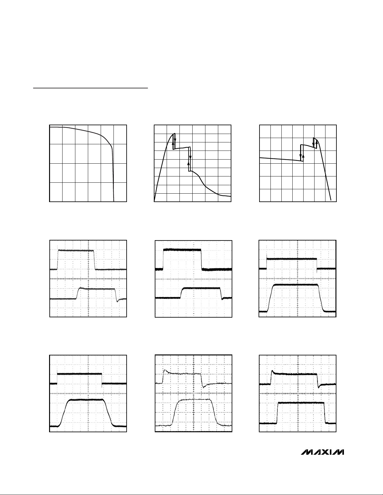
DRIVER OUTPUT CURRENT
vs. DIFFERENTIAL OUTPUT VOLTAGE
MAX3060E toc13
DIFFERENTIAL OUTPUT VOLTAGE (V)
OUTPUT CURRENT (mA)
54321
0.1
1
10
100
0.01
06
0
20
10
50
40
30
80
70
60
90
042681012
DRIVER OUTPUT CURRENT
vs. OUTPUT LOW VOLTAGE
MAX3060E toc14
OUTPUT LOW VOLTAGE (V)
DRIVER OUTPUT CURRENT (mA)
DRIVER OUTPUT CURRENT
vs. OUTPUT HIGH VOLTAGE
MAX3060E toc15
OUTPUT HIGH VOLTAGE (V)
DRIVER OUTPUT CURRENT (mA)
420-2-4-6
20
40
60
80
100
120
0
-8 6
MAX3060E toc16
RECEIVER PROPAGATION DELAY
(MAX3060E/MAX3061E)
20ns/div
V
A
- V
B
1V/div
RO
5V/div
MAX3060E toc18
DRIVER PROPAGATION DELAY
(MAX3061E)
1μs/div
V
A
- V
B
2V/div
DI
5V/div
MAX3060E toc19
DRIVER PROPAGATION DELAY
(MAX3060E)
2μs/div
V
A
- V
B
2V/div
DI
5V/div
MAX3060E toc20
DRIVER PROPAGATION DELAY
(MAX3061E)
10ns/div
V
A
- V
B
2V/div
DI
5V/div
MAX3060E toc17
RECEIVER PROPAGATION DELAY
(MAX3062E)
20ns/div
V
A
- V
B
1V/div
RO
5V/div
MAX3060E toc21
DRIVER PROPAGATION DELAY
(MAX3062E)
20ns/div
Page 11

MAX3060E/MAX3061E/MAX3062E
±15kV ESD-Protected, Fail-Safe, 20Mbps, Slew-Rate-
Limited RS-485/RS-422 Transceivers in a SOT
______________________________________________________________________________________ 11
MAX3060E/MAX3061E/MAX3062E
Detailed Description
The MAX3060E/MAX3061E/MAX3062E high-speed transceivers for RS-485/RS-422 communication contain one
driver and one receiver. These devices feature fail-safe
circuitry, which guarantees a logic-high receiver output
when the receiver inputs are open or shorted, or when
they are connected to a terminated transmission line with
all drivers disabled (see the Fail Safe section). All devices
have a hot-swap input structure that prevents disturbances on the differential signal lines when a circuit
board is plugged into a hot backplane (see the Hot-Swap
Capability section). The MAX3060E features a reduced
slew-rate driver that minimizes EMI and reduces reflections caused by improperly terminated cables, allowing
error-free data transmission up to 115kbps (see the
Reduced EMI and Reflections section). The MAX3061E is
also slew-rate limited, transmitting up to 500kbps. The
MAX3062E driver is not slew-rate limited, allowing transmit speeds up to 20Mbps. The MAX3060E/MAX3061E/
MAX3062E are half-duplex transceivers.
All of these parts operate from a single +5V supply.
Drivers are output short-circuit current limited. Thermalshutdown circuitry protects drivers against excessive
power dissipation. When activated, the thermal-shutdown circuitry places the driver outputs into a highimpedance state.
Receiver Input Filtering
The receivers of the MAX3060E and MAX3061E incorporate input filtering in addition to input hysteresis. This filtering enhances noise immunity with differential signals
that have very slow rise and fall times. Receiver propagation delay increases by 2ns due to this filtering.
Fail-Safe
The MAX3060E family of devices guarantee a logic-high
receiver output when the receiver inputs are shorted or
open, or when they are connected to a terminated transmission line with all drivers disabled. This is done by setting the receiver threshold between -50mV and
-200mV. If the differential receiver input voltage (A - B) is
greater than or equal to -50mV, RO is logic high. If
A - B is less than or equal to -200mV, RO is logic low. In
the case of a terminated bus with all transmitters disabled, the receiver’s differential input voltage is pulled to
0V by the termination. In the case of an unterminated bus
with all transmitters disabled, the receiver’s differential
input voltage is pulled to 0V by the receiver’s input resistors. With the receiver thresholds of the MAX3060E family, this results in a logic high output with a 50mV
minimum input noise margin. Unlike previous fail-safe
devices, the -50mV to -200mV threshold complies with
the ±200mV EIA/TIA-485 standard.
PIN NAME FUNCTION
1RO
Receiver Output. When RE is low and when A - B ≥ -50mV, RO is high; if A - B ≤ -200mV, RO is low. RO
is high impedance when RE is high.
2 RE
Receiver Output Enable. Drive RE low to enable RO; RO is high impedance when RE is high. Drive RE
high and DE low to enter low-power shutdown mode. RE is a hot-swap input and reverts to a standard
CMOS input after the first low transition.
3DE
Driver Output Enable. Drive DE high to enable driver outputs. Driver outputs are high impedance when
DE is low. Drive RE high and DE low to enter low-power shutdown mode. DE is a hot-swap input and
reverts to a standard CMOS input after the first high transition.
4DI
Driver Input. With DE high, a low on DI forces the noninverting output low and the inverting output high.
Similarly, a high on DI forces the noninverting output high and the inverting output low.
5 GND Ground
6 A Noninverting Receiver Input and Noninverting Driver Output
7 B Inverting Receiver Input and Inverting Driver Output
8VCCPositive Supply. Bypass with a 0.1µF capacitor to GND.
Pin Description
Page 12
MAX3060E/MAX3061E/MAX3062E
±15kV ESD-Protected, Fail-Safe, 20Mbps, Slew-RateLimited RS-485/RS-422 Transceivers in a SOT
12 ______________________________________________________________________________________
Hot-Swap Capability
Hot-Swap Input
When circuit boards are inserted into a hot or powered
backplane, differential disturbances to the data bus can
lead to data errors. Upon initial circuit board insertion, the
data communication processor undergoes its own powerup sequence. During this period, the processor’s logicoutput drivers are high impedance and are unable to
drive the DE and RE inputs of the MAX306_E to a defined
logic level. Leakage currents up to ±10µA from the highimpedance state of the processor’s logic drivers could
cause standard CMOS enable inputs of a transceiver to
drift to an incorrect logic level. Additionally, parasitic circuit board capacitance could cause coupling of VCCor
GND to the enable inputs. Without the hot-swap capability, these factors could improperly enable the transceiver’s
driver or receiver.
When VCCrises, an internal pulldown circuit holds DE
low for at least 10µs and until the current into DE
exceeds 200µA. After the initial positive transition, the
pulldown circuit becomes transparent, resetting the
hot-swap tolerable input.
Hot-Swap Input Circuitry
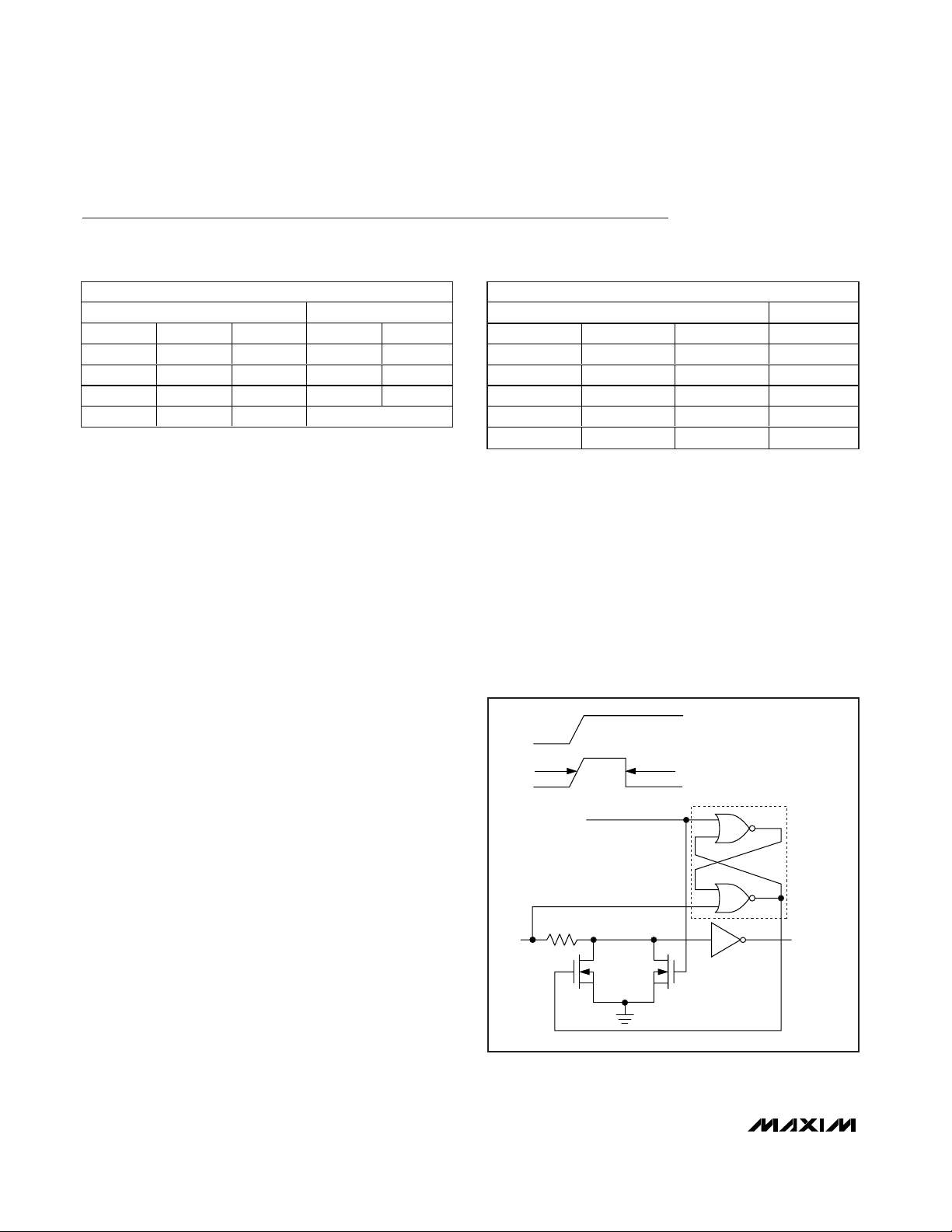
These devices’ enable inputs feature hot-swap capability. At the input there are two NMOS devices, M1 and M2
(Figure 10). When VCCramps from zero, an internal 10µs
timer turns on M2 and sets the SR latch, which also turns
on M1. Transistors M2, a 300µA current sink, and M1, a
30µA current sink, pull DE to GND through an 8kΩ resis-
tor. M2 is designed to pull DE to the disabled state
against an external parasitic capacitance up to 100pF
that can drive DE high. After 10µs, the timer deactivates
M2 while M1 remains on, holding DE low against threestate leakages that can drive DE high. M1 remains on
until an external source overcomes the required input
current. At this time, the SR latch resets and M1 turns off.
When M1 turns off, DE reverts to a standard, highimpedance CMOS input. Whenever VCCdrops below
1V, the hot-swap input is reset.
For RE, there is a complementary circuit employing two
PMOS devices pulling RE to VCC.
Functional Tables
Table 1. Transmitter Functional Table
Table 2. Receiver Functional Table
X = Don’t care.
*Shutdown mode, driver and receiver outputs are high impedance.
TRANSMITTING
INPUTS OUTPUTS
RE DE DI B A
X1101
X1010
0 0 X High-Z High-Z
1 0 X Shutdown*
Figure 10. Simplified Structure of the Driver Enable Input (DE)
RE DE A-B
0X≥ -0.05V
0X≤ -0.2V
0 X Open/shorted
1 1 X High-Z
1 0 X Shutdown
V
TIMER
CC
TIMER
RECEIVING
INPUTS OUTPUT
RO
1
0
1
10μs
SR LATCH
8kΩ
DE
300μA
30μA
M1 M2
DE
(HOT SWAP)
Page 13

Hot-Swap Line Transient
The circuit of Figure 11 shows a typical offset termination used to guarantee a greater than 200mV offset
when a line is not driven (the 50pF represents the minimum parasitic capacitance that would exist in a typical
application). During a hot-swap event when the driver
is connected to the line and is powered up, the driver
must not cause the differential signal to drop below
200mV. Figures 12, 13, and 14 show the results of the
MAX3060E during power-up for three different V
CC
ramp rates (0.1V/µs, 1V/µs, and 10V/µs). The photos
show the VCCramp, the single-ended signal on each
side of the 100Ω termination, as well as the differential
signal across the termination.
±15kV ESD Protection
As with all Maxim devices, ESD-protection structures
are incorporated on all pins to protect against ESD
encountered during handling and assembly. The
MAX3060E family’s receiver inputs/driver outputs (A, B)
have extra protection against static electricity found in
normal operation. Maxim’s engineers developed stateof-the-art structures to protect these pins against
±15kV ESD without damage. After an ESD event, the
devices continue working without latchup.
ESD protection can be tested in several ways. The
receiver inputs are characterized for protection to the
following:
• ±15kV using the Human Body Model
• ±7kV using the Contact Discharge method specified
in IEC 1000-4-2 (formerly IEC 801-2)
• ±7kV using the Air-Gap Discharge method specified
in IEC 1000-4-2 (formerly IEC 801-2)
MAX3060E/MAX3061E/MAX3062E
±15kV ESD-Protected, Fail-Safe, 20Mbps, Slew-Rate-
Limited RS-485/RS-422 Transceivers in a SOT
______________________________________________________________________________________ 13
MAX3060E/MAX3061E/MAX3062E
DI
5.0V
V
CC
0.1kΩ
1kΩ
1kΩ
V
CC
OR GND
A
B
50pF
Figure 11. Typical Offset Termination
40μs/div
5V
238mV
20mV/div
200mV/div
0
200mV/div
B
V
CC
A
A - B
Figure 12. Differential Power-Up Glitch (0.1V/µs)
2μs/div
B
V
CC
238mV
20mV/div
5V
A
A - B
20mV/div
20mV/div
0
Figure 13. Differential Power-Up Glitch (1V/µs)
200ns/div
B
V
CC
238mV
20mV/div
5V
A
A - B
50mV/div
50mV/div
0
Figure 14. Differential Power-Up Glitch (10V/µs)
Page 14

MAX3060E/MAX3061E/MAX3062E
±15kV ESD-Protected, Fail-Safe, 20Mbps, Slew-RateLimited RS-485/RS-422 Transceivers in a SOT
14 ______________________________________________________________________________________
ESD Test Conditions
ESD performance depends on a number of conditions.
Contact Maxim for a reliability report that documents
test setup, methodology, and results.
Human Body Model
Figure 15a shows the Human Body Model, and Figure
15b shows the current waveform it generates when discharged into a low impedance. This model consists of
a 100pF capacitor charged to the ESD voltage of interest, which is then discharged into the device through a
1.5kΩ resistor.
IEC 1000-4-2
The IEC 1000-4-2 standard covers ESD testing and performance of finished equipment; it does not specifically
refer to integrated circuits.
The main difference between tests done using the
Human Body Model and IEC 1000-4-2 is higher peak
current in IEC 1000-4-2. Because series resistance is
lower in the IEC 1000-4-2 ESD test model (Figure 16), the
ESD withstand voltage measured to this standard is generally lower than that measured using the Human Body
Model. The Air-Gap test involves approaching the
device with a charged probe. The Contact Discharge
method connects the probe to the device before the
probe is energized.
Machine Model
The Machine Model for ESD testing uses a 200pF storage capacitor and zero-discharge resistance. It mimics
the stress caused by handling during manufacturing
and assembly. All pins (not just RS-485 inputs) require
this protection during manufacturing. Therefore, the
Machine Model is less relevant to the I/O ports than are
the Human Body Model and IEC 1000-4-2.
Applications Information
256 Transceivers on the Bus
The standard RS-485 receiver input impedance is 12kΩ
(one-unit load), and the standard driver can drive up to
32-unit loads. The MAX3060E family of transceivers have
a 1/8-unit-load receiver input impedance (96kΩ), allowing up to 256 transceivers to be connected in parallel on
one communication line. Any combination of these
devices and/or other RS-485 transceivers with a total of
32 unit loads or less can be connected to the line.
Reduced EMI and Reflections
The MAX3060E and MAX3061E are slew-rate limited,
minimizing EMI and reducing reflections caused by
improperly terminated cables. Figure 17 shows the driver output waveform and its Fourier analysis of a 25kHz
signal transmitted by a MAX3062E. High-frequency
harmonic components with large amplitudes are evident. Figure 18 shows the same signal displayed for a
MAX3061E transmitting under the same conditions.
CHARGE-CURRENT
LIMIT RESISTOR
DISCHARGE
RESISTANCE
STORAGE
CAPACITOR
C
s
100pF
R
C
1MΩ
R
D
1.5kΩ
HIGH-
VOLTAGE
DC
SOURCE
DEVICE
UNDER
TEST
Figure 15a. Human Body ESD Test Model
IP 100%
90%
36.8%
t
RL
TIME
t
DL
CURRENT WAVEFORM
PEAK-TO-PEAK RINGING
(NOT DRAWN TO SCALE)
I
r
10%
0
0
AMPERES
Figure 15b. Human Body Current Waveform
CHARGE-CURRENT
LIMIT RESISTOR
DISCHARGE
RESISTANCE
STORAGE
CAPACITOR
C
s
150pF
R
C
50MΩ to 100MΩ
RD
330Ω
HIGH-
VOLTAGE
DC
SOURCE
DEVICE
UNDER
TEST
Figure 16. IEC 1000-4-2 ESD Test Model
Page 15

Figure 18’s high-frequency harmonic components are
much lower in amplitude, compared with Figure 17’s,
and the potential for EMI is significantly reduced. Figure
19 shows the same signal displayed for a MAX3060E
transmitting under the same conditions. Figure 19’s
high-frequency harmonic components are even lower.
In general, a transmitter’s rise time relates directly to the
length of an unterminated stub, which can be driven with
only minor waveform reflections. The following equation
expresses this relationship conservatively:
Length = t
RISE
/ (10 x 1.5ns/ft)
where t
RISE
is the transmitter’s rise time.
For example, the MAX3060E’s rise time is typically
1850ns, which results in excellent waveforms with a stub
length up to 123ft. A system can work well with longer
unterminated stubs, even with severe reflections, if the
waveform settles out before the UART samples them.
Low-Power Shutdown Mode
Low-power shutdown mode is initiated by bringing both
RE high and DE low. In shutdown, the devices typically
draw only 1nA of supply current.
RE and DE can be driven simultaneously. The parts are
guaranteed not to enter shutdown if RE is high and DE is
low for less than 50ns. If the inputs are in this state for at
least 600ns, the parts are guaranteed to enter shutdown.
Enable times t_
ZH
and t_ZLin the Switching Char-
acteristics tables assume the part was not in a lowpower shutdown state. Enable times t_
ZH(SHDN)
and
t_
ZL(SHDN)
assume the parts were shut down. It takes
drivers and receivers longer to become enabled from
low-power shutdown mode (t_
ZH(SHDN)
, t_
ZL(SHDN)
)
than from driver/receiver-disable mode (t_
ZH
, t_ZL).
Driver Output Protection
Two mechanisms prevent excessive output current and
power dissipation caused by faults or by bus contention. The first, a foldback current limit on the output
stage, provides protection after a 20µs delay against
short circuits over the whole common-mode voltage
range (see Typical Operating Characteristics). The sec-
ond, a thermal shutdown circuit, forces the driver outputs into a high-impedance state if the die temperature
becomes excessive.
MAX3060E/MAX3061E/MAX3062E
±15kV ESD-Protected, Fail-Safe, 20Mbps, Slew-Rate-
Limited RS-485/RS-422 Transceivers in a SOT
______________________________________________________________________________________ 15
MAX3060E/MAX3061E/MAX3062E
125kHz/div
20dB/div
0
1.25MHz
Figure 17. Driver Output Waveform and FFT Plot of MAX3062E
Transmitting a 25kHz Signal
125kHz/div
20dB/div
0
1.25MHz
Figure 18. Driver Output Waveform and FFT Plot of MAX3061E
Transmitting a 25kHz Signal
125kHz/div
20dB/div
0
1.25MHz
Figure 19. Driver Output Waveform and FFT Plot of MAX3060E
Transmitting a 25kHz Signal
Page 16
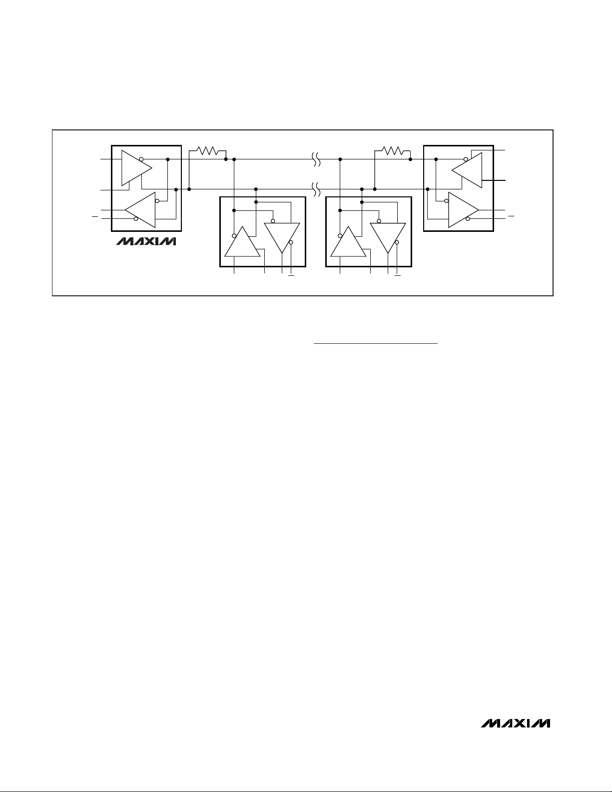
Typical Applications
The MAX3060E family of transceivers are designed for
bidirectional data communications on multipoint bus
transmission lines. Figure 20 shows a typical network
application circuit.
To minimize reflections, the line should be terminated at
both ends in its characteristic impedance, and stub
lengths off the main line should be kept as short as
possible. The slew-rate-limited MAX3060E and
MAX3061E are more tolerant of imperfect termination.
Chip Information
PROCESS: CMOS
MAX3060E/MAX3061E/MAX3062E
±15kV ESD-Protected, Fail-Safe, 20Mbps, Slew-RateLimited RS-485/RS-422 Transceivers in a SOT
16 ______________________________________________________________________________________
DI RO DE
RE
A
B
RE
RERE
RO
RO
RO
DI
DI
DI
DE
DE
DE
D
D
D
R
R
R
B
B
B
A
A
A
120Ω
120Ω
D
R
MAX3060E/MAX3061E/
MAX3062E
(HALF-DUPLEX)
Figure 20. Typical Half-Duplex RS-485 Network
Page 17

±15kV ESD-Protected, Fail-Safe, 20Mbps, Slew-Rate-
Limited RS-485/RS-422 Transceivers in a SOT
MAX3060E/MAX3061E/MAX3062E
Maxim cannot assume responsibility for use of any circuitry other than circuitry entirely embodied in a Maxim product. No circuit patent licenses are
implied. Maxim reserves the right to change the circuitry and specifications without notice at any time.
Maxim Integrated Products, 120 San Gabriel Drive, Sunnyvale, CA 94086 408-737-7600 ____________________ 17
© 2007 Maxim Integrated Products is a registered trademark of Maxim Integrated Products, Inc.
MAX3060E/MAX3061E/MAX3062EMAX3060E/MAX3061E/MAX3062E
Package Information
(The package drawing(s) in this data sheet may not reflect the most current specifications. For the latest package outline information
go to www.maxim-ic.com/packages
.)
Revision History
Pages changed at Rev 1: 1, 16, 17
MARKING
0
SOT23, 8L.EPS
0
PACKAGE OUTLINE, SOT-23, 8L BODY
21-0078 G
1
1
 Loading...