

General Description
The MAX3050/MAX3057 interface between the CAN
protocol controller and the physical wires of the bus
lines in a controller area network (CAN). They are primarily intended for automotive systems requiring data
rates up to 2Mbps and feature ±80V fault protection
against short circuits in high-voltage power buses. They
provide differential transmit capability to the bus and
differential receive capability to the CAN controller.
The MAX3050/MAX3057 have four modes of operation:
high speed, slope control, standby, and shutdown.
High-speed mode allows data rates up to 2Mbps. In
slope-control mode, data rates are 40kbps to 500kbps,
so the effects of EMI are reduced, and unshielded
twisted or parallel cable can be used. In standby mode,
the transmitters are shut off and the receivers are put
into low-current mode. In shutdown mode, the transmitter and receiver are switched off.
The MAX3050 has an AutoShutdown™ function that
puts the device into a 15µA shutdown mode when the
bus or CAN controller is inactive for 4ms or longer.
The MAX3050/MAX3057 are available in an 8-pin SO
package and are specified for operation from -40°C to
+125°C.
Applications
Automotive Systems
HVAC Controls
Telecom 72V systems
Features
♦ ±80V Fault Protection for 42V Systems
♦ Four Operating Modes
High-Speed Operation Up to 2Mbps
Slope-Control Mode to Reduce EMI
(40kbps to 500kbps)
Standby Mode
Low-Current Shutdown Mode
♦ AutoShutdown when Device Is Inactive
(MAX3050)
♦ Automatic Wake-Up from Shutdown (MAX3050)
♦ Thermal Shutdown
♦ Current Limiting
♦ Fully Compatible with the ISO 11898 Standard*
MAX3050/MAX3057
±80V Fault-Protected, 2Mbps, Low Supply
Current CAN Transceivers
________________________________________________________________ Maxim Integrated Products 1
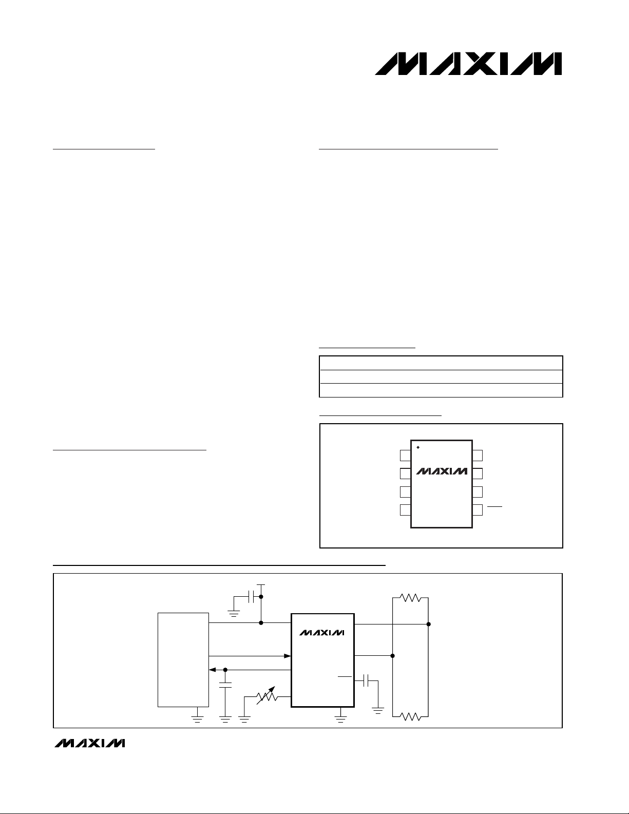
Ordering Information
MAX3050
MAX3057
CAN
CONTROLLER
TXD
V
CC
RXD
RS
GND
CANH
CANL
V
CC
(100nF)
120Ω
120Ω
TX0
RX0
GND
0.1µF
30pF
24kΩ TO 180kΩ
SHDN
( ) ARE FOR 3050 ONLY.
Typical Operating Circuit
19-2670; Rev 0; 10/02
For pricing, delivery, and ordering information, please contact Maxim/Dallas Direct! at
1-888-629-4642, or visit Maxim’s website at www.maxim-ic.com.
Pin Configuration
AutoShutdown is a trademark of Maxim Integrated Products, Inc.
* Pending completion of testing.
PART TEMP RANGE PIN-PACKAGE
MAX3050ASA -40°C to +125°C 8 SO
MAX3057ASA -40°C to +125°C 8 SO
TOP VIEW
TXD
V
RXD
1
2
MAX3050
MAX3057
3
CC
4
SO
87RS
6
5
CANHGND
CANL
SHDN
MAX3050/MAX3057
±80V Fault-Protected, 2Mbps, Low Supply
Current CAN Transceivers
2 _______________________________________________________________________________________
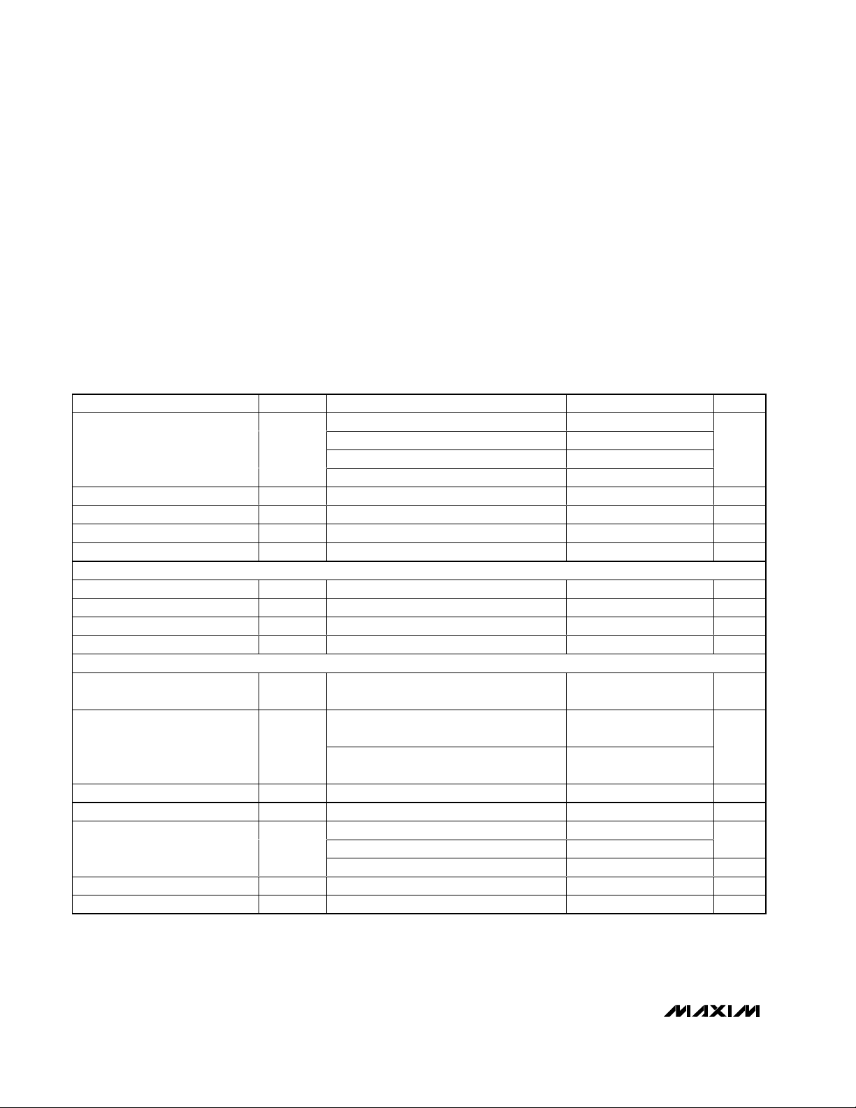
ABSOLUTE MAXIMUM RATINGS
DC ELECTRICAL CHARACTERISTICS
(VCC= +5V ±10%, RL= 60Ω, RS = GND, TA= T
MIN
to T
MAX
. Typical values are at VCC= +5V and TA= +25°C.)
Stresses beyond those listed under “Absolute Maximum Ratings” may cause permanent damage to the device. These are stress ratings only, and functional
operation of the device at these or any other conditions beyond those indicated in the operational sections of the specifications is not implied. Exposure to
absolute maximum rating conditions for extended periods may affect device reliability.
VCCto GND ............................................................ -0.3V to +6V
TXD, RS, RXD, SHDN to GND ....................-0.3V to (V
CC
+ 0.3V)
CANH, CANL to GND..............................................-80V to +80V
RXD Shorted to GND................................................. Continuous
Continuous Power Dissipation (T
A
= +70°C)
8-Pin SO (derate 5.9mW/°C above +70°C) .................470mW
Operating Temperature Range .........................-40°C to +125°C
Junction Temperature......................................................+150°C
Storage Temperature Range .............................-65°C to +150°C
Lead Temperature (soldering, 10s) ................................+300°C
Supply Current I
Quiescent Current Standby Mode I
Shutdown Supply Current I
PARAMETER SYMBOL CONDITIONS MIN TYP MAX UNITS
S
Q
QSHDN
Thermal-Shutdown Threshold 160 °C
Thermal-Shutdown Hysteresis 20 °C
TXD INPUT LEVELS
High-Level Input Voltage V
Low-Level Input Voltage V
High-Level Input Current I
Pullup Resistor R
IH
IL
IH
INTXD
CANH, CANL TRANSMITTER
V
Recessive Bus Voltage
Off-State Output Leakage I
CANH Output Voltage V
CANL Output Voltage V
Differential Output
(V
CANH
- V
CANL
)
CANH Short-Circuit Current I
CANL Short-Circuit Current I
CANH,
V
CANL
LO
CANHVTXD
CANL
∆V
CANH
V
CANL
SC
SC
Dominant (Note 1) 56 72
Dominant no load 6
Recessive (Note 1) 3.6 5.5
Recessive no load 5.5
V
= V
RS
CC
SHDN = GND 15 30 µA
V
= V
TXD
CC
V
= VCC, no load 2 3 V
TXD
-2V < V
CANH
SHDN = GND, V
-80V < V
CANH
SHDN = GND, V
= 0 3.0 V
V
= 0 0 2.0 V
TXD
V
= 0 1.5 5
TXD
,
V
= 0, RL = 45Ω 1.5
TXD
V
= VCC, no load -500 +50 mV
TXD
V
= -5V -200 mA
CANH
V
= 18V 200 mA
CANL
125 260 µA
2V
0.4 V
1µA
20 kΩ
, V
< +7V
CANL
, V
TXD
CANL
TXD
= V
< +80V
= V
CC
CC
-2 +1
-4 +4
CC
mA
mA
V
V
MAX3050/MAX3057
±80V Fault-Protected, 2Mbps, Low Supply
Current CAN Transceivers
_______________________________________________________________________________________ 3
DC ELECTRICAL CHARACTERISTICS (continued)
(VCC= +5V ±10%, RL= 60Ω, RS = GND, TA= T
MIN
to T
MAX
. Typical values are at VCC= +5V and TA= +25°C.)
)
DC BUS RECEIVER (V
Differential Input Voltage
(Recessive)
Differential Input Voltage
(Dominant)
Differential Input Hysteresis V
CANH Input Wake-Up Voltage
Threshold
RXD High-Level Output Voltage V
RXD Low-Level Output Voltage V
CANH and CANL Input
Resistance
Differential Input Resistance R
PARAMETER SYMBOL CONDITIONS MIN TYP MAX UNITS
= VCC; CANH and CANL externally driven; -2V < V
TXD
V
DIFF
V
DIFF
DIFF(HYST
V
CANH
(SHDN)
OH
OL
R
I
DIFF
-7V < V
-7V < V
SHDN = GND, V
, V
CANH
CANH
< +12V -1.0 +0.5 V
CANL
, V
< +12V 0.9 3.3 V
CANL
= V
TXD
I = -100µA
I = 10mA 0.8
I = 5mA 0.4
, V
CANH
< +7V, unless otherwise specified)
CANL
150 mV
(MAX3050) 6 9 V
CC
0.8
✕
V
CC
525kΩ
10 100 kΩ
V
V
MODE SELECTION (RS)
Input Voltage for High Speed V
Input Voltage for Standby V
Slope-Control Mode Voltage V
Slope-Control Mode Current I
Standby Mode I
High-Speed Mode Current I
SLP
STBY
SLOPERRS
SLOPE
STBY
HS
RRS = 24kΩ to 180kΩ -200 -10 µA
V
0.75 ✕
V
CC
0.4
= 24kΩ to 180kΩ
✕
V
CC
-10 +10 µA
= 0 -500 µA
RS
0.3 ✕
V
CC
0.6 ✕
V
CC
V
V
V
SHUTDOWN
SHDN Input Pullup Resistor R
INSHDN
MAX3057 500 900 kΩ
SHDN Input Voltage High 2V
SHDN Input Voltage Low 0.5 V
MAX3050/MAX3057
±80V Fault-Protected, 2Mbps, Low Supply
Current CAN Transceivers
4 _______________________________________________________________________________________
Note 1: As defined by ISO, bus value is one of two complementary logical values: dominant or recessive. The dominant value repre-
sents the logical 1 and the recessive represents the logical 0. During the simultaneous transmission of the dominant and
recessive bits, the resulting bus value is dominant. For MAX3050 and MAX3057 values, see the truth table in the
Transmitter and Receiver sections.
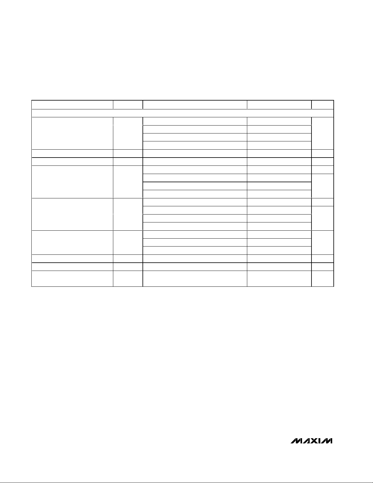
TIMING CHARACTERISTICS
(VCC= +5V ±10%, RL= 60Ω, CL= 100pF, TA= T
MIN
to T
MAX
. Typical values are at VCC= +5V and TA= +25°C.) (Figures 1, 2, and 3)
TIMING
Minimum Bit Time t
Delay TXD to Bus Active t
Delay TXD to Bus Inactive t
Delay TXD to Receiver Active t
Delay TXD to Receiver Inactive t
Bus Dominant to RXD Low Standby mode 10 µs
Time to Wake Up: CANH > 9V t
Time to Sleep Mode when Bus Is
Recessive
PARAMETER SYMBOL CONDITIONS MIN TYP MAX UNITS
BIT
ONTXDVRS
OFFTXDVRS
ONRXD
OFFRXD
WAKE
t
SHDN
V
RS
RRS = 24kΩ (500kbps) 2
RRS = 100kΩ (125kbps) 8
RRS = 180kΩ (62.5kbps) 25
V
RS
RRS = 24kΩ (500kbps) 0.4
RRS = 100kΩ (125kbps) 1.6
RRS = 180kΩ (62.5kbps) 5.0
V
RS
RRS = 24kΩ (500kbps) 0.45
RRS = 100kΩ (125kbps) 1.6
RRS = 180kΩ (62.5kbps) 5.0
RRS = 24kΩ (500kbps) 14
RRS = 100kΩ (125kbps) 7Differential Output Slew Rate SR
R
RS
SHDN = GND, V
C
SHDN
= 0 (2Mbps) 0.5
= 0 40 ns
= 0 75 ns
= 0 (2Mbps) 120 ns
= 0 (2Mbps) 130 ns
= 180kΩ (62.5kbps) 1.6
= V
TXD
= 100nF (MAX3050) 10 47 ms
(MAX3050) 10 µs
CC
µs
µs
µs
V/µs

MAX3050/MAX3057
±80V Fault-Protected, 2Mbps, Low Supply
Current CAN Transceivers
_______________________________________________________________________________________ 5
Figure 1. AC Test Circuit
Figure 2. Timing Diagram for Dynamic Characteristics
Figure 3. Time to Wake Up (t
WAKE
) (MAX3050)
CAN
CONTROLLER
TXD
CANH
CANL
CANH - CANL
GND
TX0
RX0
DOMINANT
0.1µF
30pF
24kΩ TO 180kΩ
V
CC
0.5V
V
CC
TXD
RXD
RS
RECESSIVE
MAX3050
MAX3057
0.9V
GND
CANH
CANL
SHDN
100pF
(100nF)
CANH
V
SHDN
120Ω
120Ω
( ) ARE FOR MAX3050 ONLY.
V
= 2V
SHDN
9V
V
/2
RXD
t
ONTXD
t
ONRXD
CC
V
/2
CC
t
OFFTXD
t
OFFRXD
t
WAKE

MAX3050/MAX3057
±80V Fault-Protected, 2Mbps, Low Supply
Current CAN Transceivers
6 _______________________________________________________________________________________
Typical Operating Characteristics
(VCC= 5V, RL= 60Ω, CL= 100pF, TA= +25°C, unless otherwise specified.)
MAX3057
SLEW RATE vs. R
RS
MAX3050 toc01
RRS (kΩ)
SLEW RATE (V/µs)
1621248648
5
10
15
20
25
0
10 200
TA = -40°C
TA = +25°C
TA = -+125°C
MAX3050 toc02
SLEEP TIME (ms)
300200100
20
40
60
80
100
0
0 400
MAX3050
AutoShutdown vs. C
SHDN
C
SHDN
(nF)
SUPPLY CURRENT vs. DATA RATE
MAX3050 toc03
DATA RATE (kbps)
SUPPLY CURRENT (mA)
16001200800400
27
29
31
33
35
25
0 2000
TA = +125°C
TA = +25°C
TA = -40°C
RECEIVER PROPAGATION DELAY
vs. TEMPERATURE, R
RS
= GND
MAX3050 toc04
TEMPERATURE (°C)
RECEIVER PROPAGATION DELAY (ns)
905520-15
25
35
45
55
65
15
-50 125
RECESSIVE
DOMINANT
DRIVER PROPAGATION DELAY
vs. TEMPERATURE, R
RS
= GND
MAX3050 toc05
TEMPERATURE (°C)
DRIVER PROPAGATION DELAY (ns)
925926-7
20
25
30
35
15
-40 125
RECESSIVE
DOMINANT
RECEIVER OUTPUT LOW
vs. OUTPUT CURRENT
MAX3050 toc06
OUTPUT CURRENT (mA)
VOLTAGE RXD (mV)
2015105
400
800
1200
1600
0
025
TA = +125°C
TA = +25°C
TA = -40°C
RECEIVER OUTPUT HIGH
vs. OUTPUT CURRENT
MAX3050 toc07
OUTPUT CURRENT (mA)
VOLTAGE (V
CC
- RXD) (mV)
2015105
600
1200
1800
3000
2400
0
025
TA = +125°C
TA = +25°C
TA = -40°C
DIFFERENTIAL VOLTAGE
vs. DIFFERENTIAL LOAD R
L
MAX3050 toc08
DIFFERENTIAL LOAD RL (Ω)
DIFFERENTIAL VOLTAGE (V)
25020015010050
1
2
3
4
0
0 300
TA = +125°C
TA = +25°C
TA = -40°C
SUPPLY CURRENT
vs. TEMPERATURE IN STANDBY MODE
MAX3050 toc09
TEMPERATURE (°C)
SUPPLY CURRENT (µA)
905520-15
75
100
125
150
175
200
50
-50 125

MAX3050/MAX3057
±80V Fault-Protected, 2Mbps, Low Supply
Current CAN Transceivers
_______________________________________________________________________________________ 7
Typical Operating Characteristics (continued)
(VCC= 5V, RL= 60Ω, CL= 100pF, TA= +25°C, unless otherwise specified.)
Pin Description
LOOPBACK PROPAGATION DELAY vs. R
1400
1200
1000
800
600
400
LOOPBACK PROPAGATION DELAY (ns)
200
0
0 200
RRS (kΩ)
DRIVER PROPAGATION DELAY
15010050
MAX3050 toc12
RS
MAX3050 toc10
TXD
2V/div
CANH - CANL
RECEIVER PROPAGATION DELAY
40ns/div
DRIVER PROPAGATION DELAY
MAX3050 toc11
MAX3050 toc13
CANH - CANL
RXD
2V/div
TXD
5V/div
= 24kΩ
R
RS
= 100kΩ
R
RS
= 180kΩ
R
RS
RRS = GND
40ns/div
PIN NAME FUNCTION
1µs/div
1 TXD Transmit Data Input. TXD is a CMOS/TTL-compatible input from a CAN controller.
2 GND Ground
3VCCSupply Voltage. Bypass V
to GND with a 0.1µF capacitor.
CC
4 RXD Receive Data Output. RXD is a CMOS/TTL-compatible output from the physical bus lines CANH and CANL.
Shutdown Input. Drive SHDN low to put into shutdown mode (MAX3057). Place a capacitor from SHDN to
5 SHDN
ground to utilize the AutoShutdown feature of MAX3050. See the Shutdown and AutoShutdown sections for a
full explanation of SHDN behavior.
6 CANL CAN Bus Line Low. CANL is fault protected to ±80V.
7 CANH CAN Bus Line High. CANH is fault protected to ±80V.
8RS
Mode Select Pin. Drive RS low or connect to GND for high-speed operation. Connect a resistor from RS to
GND to control output slope. Drive RS high to put into standby mode. See the Mode Selection section.

MAX3050/MAX3057
Detailed Description
The MAX3050/MAX3057 interface between the protocol
controller and the physical wires of the bus lines in a
CAN. They are primarily intended for automotive applications requiring data rates up to 2Mbps and feature
±80V fault protection against shorts in high-voltage systems. This fault protection allows the devices to withstand up to ±80V with respect to ground with no
damage to the device. The built-in fault tolerance
allows the device to survive in industrial and automotive
environments with no external protection devices. The
devices provide differential transmit capability to the
bus and differential receive capability to the CAN controller (Figure 4).
The device has four modes of operation: high speed,
slope control, standby, and shutdown. In high-speed
mode, slew rates are not limited, making 2Mbps transmission speeds possible. Slew rates are controlled in slopecontrol mode, minimizing EMI and allowing use of
unshielded twisted or parallel cable. In standby mode,
receivers are active and transmitters are in high impedance. In shutdown mode, transmitters and receivers are
turned off.
The transceivers are designed to operate from a single
+5V supply and draw 56mA of supply current in dominant state and 3.6mA in recessive state. In standby
mode, supply current is reduced to 125µA. In shutdown
mode, supply current is 15µA.
CANH and CANL are output short-circuit current limited
and are protected against excessive power dissipation
by thermal-shutdown circuitry that places the driver
outputs into a high-impedance state.
Fault Protection
The MAX3050/MAX3057 feature ±80V fault protection.
This extended voltage range of CANH and CANL bus
lines allows use in high-voltage systems and communication with high-voltage buses. If data is transmitting at
2Mbps, the fault protection is reduced to ±70V.
Transmitter
The transmitter converts a single-ended input (TXD)
from the CAN controller to differential outputs for the
bus lines (CANH, CANL). The truth table for the transmitter and receiver is given in Table 1.
±80V Fault-Protected, 2Mbps, Low Supply
Current CAN Transceivers
8 _______________________________________________________________________________________
Figure 4. Functional Diagram
THERMAL
SHUTDOWN
V
CC
MAX3050
CANH
TXD
RS
RXD
MODE
SELECTION
TRANSMITTER
CONTROL
RECEIVER
0.75V
7.5V
WAKE
AutoShutdown
CANL
GND
SHDN

High Speed
Connect RS to ground to set the MAX3050/MAX3057 to
high-speed mode. When operating in high-speed
mode, the MAX3050/MAX3057 can achieve transmission rates of up to 2Mbps. Line drivers are switched on
and off as quickly as possible. However, in this mode,
no measures are taken to limit the rise and fall slope of
the data signal, allowing for potential EMI emissions. If
using the MAX3050/MAX3057 in high-speed mode, use
shielded twisted-pair cable to avoid EMI problems.
Slope Control
Connect a resistor from RS to ground to select slopecontrol mode (Table 2). In slope-control mode, the
gates of the line drivers are charged with a controlled
current, proportional to the resistor connected to the RS
pin. Transmission speed ranges from 40kbps to
500kbps. Controlling the rise and fall slope reduces
EMI and allows the use of an unshielded twisted pair or
a parallel pair of wires as bus lines. The transfer function for selecting the resistor value is given by:
RRS(kΩ) = 12000/speed (in kbps)
See the Slew Rate vs. RRSgraph in the Typical
Operating Characteristics section.
Receiver
The receiver reads differential input from the bus lines
(CANH, CANL) and transfers this data as a singleended output (RXD) to the CAN controller. It consists of
a comparator that senses the difference ∆V = (CANH CANL) with respect to an internal threshold of 0.7V. If
this difference is positive (i.e., ∆V > 0.7V), a logic low is
present at the RXD pin. If negative (i.e., ∆V < 0.7V), a
logic high is present.
The receiver always echoes the transmitted data.
The CANH and CANL common-mode range is -7V to
+12V. RXD is logic high when CANH and CANL are
shorted or terminated and undriven. If the differential
receiver input voltage (CANH - CANL) is less than or
equal to 0.5V, RXD is logic high. If (CANH - CANL) is
greater than or equal to 0.9V, RXD is logic low.
Standby
If a logic high level is applied to RS, the MAX3050/
MAX3057 enter a low-current standby mode. In this
mode, the transmitter is switched off and the receiver is
switched to a low-current state. If dominant bits are
detected, RXD switches to a low level. The microcontroller should react to this condition by switching the
transceiver back to normal operation (through RS). Due
to the reduced power mode, the receiver is slower in
standby mode, and the first message may be lost at
higher bit rates.
Thermal Shutdown
If the junction temperature exceeds +160°C, the device
is switched off. The hysteresis is approximately 20°C,
disabling thermal shutdown once the temperature
reaches +140°C.
Shutdown (MAX3057)
Drive SHDN low to enter shutdown mode. In shutdown
mode, the device is switched off. The outputs are high
impedance to ±80V. The MAX3057 features a pullup at
SHDN. If shutdown is forced low and then left floating,
the device switches back to normal operating mode.
MAX3050/MAX3057
±80V Fault-Protected, 2Mbps, Low Supply
Current CAN Transceivers
_______________________________________________________________________________________ 9
Table 1. Transmitter and Receiver Truth Table
X = Don’t care.
*As defined by ISO, bus value is one of two complementary logical values: dominant or recessive. The dominant value represents the
logical 0 and the recessive represents the logical 1. During the simultaneous transmission of the dominant and recessive bits, the resulting bus value is dominant.
Table 2. Mode Selection Truth Table
TXD RS SHDN CANH CANL BUS STATE RXD
0V
1 or float VRS < 0.75 ✕ V
XV
XXV
< 0.75 ✕ V
RS
> 0.75 ✕ V
RS
CC
CC
CC
V
> 1.5V High Low Dominant* 0
S HDN
V
> 1.5V 5kΩ to 25kΩ to VCC/2 5kΩ to 25kΩ to VCC/2 Recessive* 1
S HDN
X Floating Floating Floating 1
< 0.5V Floating Floating Floating 1
S H D N
CONDITION FORCED AT PIN RS MODE RESULTING CURRENT AT RS
VRS < 0.3 ✕ V
0.4 ✕ VCC< VRS < 0.6 ✕ V
VRS > 0.75 ✕ V
CC
CC
CC
High speed |IRs| < 500µA
Slope control 10µA < |IRs| < 200µA
Standby |IRs| < 10µA

MAX3050/MAX3057
AutoShutdown (MAX3050)
To manage power consumption, AutoShutdown puts
the device into shutdown mode after the device has
been inactive for a period of time. The value of an
external capacitor (C
SHDN
) connected to SHDN deter-
mines the threshold of inactivity time, after which the
AutoShutdown triggers. Floating SHDN allows the
MAX3050 to automatically change from active mode to
shutdown.
Use a 100nF capacitor as C
SHDN
for a typical threshold of 20ms. Change the capacitor value according to
the following equation to change the threshold time
period.
V
SHDN
is the threshold of SHDN guaranteed to be less
than 2V in the Electrical Characteristics table. Drive
SHDN high to turn the MAX3050 on and disable
AutoShutdown.
When the MAX3050 is in shutdown mode, only the
wake-up comparator is active, and normal bus communication is ignored. The remote master of the CAN system wakes up the MAX3050 with a signal greater than
9V on CANH. Internal circuitry in the MAX3050 puts the
device in normal operation by driving SHDN high.
The MAX3057 does not have the AutoShutdown feature.
Driver Output Protection
The MAX3050/MAX3057 have several features that protect them from damage. Thermal shutdown switches off
the device and puts CANH and CANL into high impedance if the junction temperature exceeds +160°C.
Thermal protection is needed particularly when a bus
line is short circuited. The hysteresis for the thermal
shutdown is approximately 20°C.
Additionally, a current-limiting circuit protects the transmitter output stage against short-circuits to positive and
negative battery voltage. Although the power dissipation increases during this fault condition, this feature
prevents destruction of the transmitter output stage.
±80V Fault-Protected, 2Mbps, Low Supply
Current CAN Transceivers
10 ______________________________________________________________________________________
Figure 5. FFT Dominant Bus at 2Mbps
Figure 6. FFT Recessive Bus at 2Mbps
Figure 7. FFT Dominant Bus at 500kbps
CnF
SHDN
002
time s
.()
()
=
×µ
VV
−
()
CC
SHDN
CANH - CANL
1V/div
FFT
500mV/div
CANH - CANL
1V/div
FFT
200mV/div
CANH - CANL
1V/div
FFT
500mV/div

Applications Information
Reduced EMI and Reflections
In slope-control mode, the CANH and CANL outputs
are slew-rate limited, minimizing EMI and reducing
reflections caused by improperly terminated cables. In
general, a transmitter’s rise time relates directly to the
length of an unterminated stub, which can be driven
with only minor waveform reflections. The following
equation expresses this relationship conservatively:
Length = t
RISE
/ (15ns/ft)
where t
RISE
is the transmitter’s rise time.
The MAX3050 and MAX3057 require no special layout
considerations beyond common practices. Bypass V
CC
to GND with a 0.1µF ceramic capacitor mounted close
to the IC with short lead lengths and wide trace widths.
Chip Information
TRANSISTOR COUNT: 1214
PROCESS: BiCMOS
MAX3050/MAX3057
±80V Fault-Protected, 2Mbps, Low Supply
Current CAN Transceivers
______________________________________________________________________________________ 11
Figure 8. FFT Recessive Bus at 500kbps
Figure 9. FFT Dominant Bus at 62.5kbps
Figure 10. FFT Recessive Bus at 62.5kbps
CANH - CANL
1V/div
FFT
200mV/div
CANH - CANL
1V/div
FFT
500mV/div
CANH - CANL
1V/div
FFT
200mV/div

MAX3050/MAX3057
±80V Fault-Protected, 2Mbps, Low Supply
Current CAN Transceivers
Maxim cannot assume responsibility for use of any circuitry other than circuitry entirely embodied in a Maxim product. No circuit patent licenses are
implied. Maxim reserves the right to change the circuitry and specifications without notice at any time.
12 ____________________Maxim Integrated Products, 120 San Gabriel Drive, Sunnyvale, CA 94086 408-737-7600
© 2002 Maxim Integrated Products Printed USA is a registered trademark of Maxim Integrated Products.
Package Information
(The package drawing(s) in this data sheet may not reflect the most current specifications. For the latest package outline information,
go to www.maxim-ic.com/packages.)
N
HE
1
TOP VIEW
D
A
e
FRONT VIEW
B
A1
INCHES
DIM
MIN
0.053A
0.004
A1
0.014
B
0.007
C
e 0.050 BSC 1.27 BSC
0.150
E
H 0.2440.228 5.80 6.20
0.016L
VARIATIONS:
INCHES
MINDIM
D
0.189 0.197 AA5.004.80 8
0.337 0.344 AB8.758.55 14
D
C
L
0-8
MAX
0.069
0.010
0.019
0.010
0.157
0.050
MAX
0.3940.386D
MILLIMETERS
MAX
MIN
1.35
1.75
0.10
0.25
0.35
0.49
0.19
0.25
3.80 4.00
0.40 1.27
MILLIMETERS
MAX
MIN
9.80 10.00
SOICN .EPS
N MS012
16 AC
SIDE VIEW
PROPRIETARY INFORMATION
TITLE:
PACKAGE OUTLINE, .150" SOIC
REV.DOCUMENT CONTROL NO.APPROVAL
21-0041
1
B
1
 Loading...