

Page 1
General Description
The MAX3054/MAX3055/MAX3056 are interfaces
between the protocol controller and the physical wires
of the bus lines in a controller area network (CAN). The
devices provide differential transmit capability and
switch to single-wire mode if certain fault conditions
occur. The MAX3054/MAX3055/MAX3056 guarantee
full wake-up capability during failure modes.
The extended fault-protected voltage range of CANH
and CANL bus lines of ±80V allows for use in 42V
automotive applications. Current-limiting and thermalprotection circuits protect the transmitter output stage
against overcurrent faults to prevent destruction of the
transmitter output stage. The CANH and CANL lines are
also protected against electrical transients that may occur
in an automotive environment.
The transceiver provides three low-power modes that
can be entered and exited through pins STB and EN.
An output INH pin can be used for deactivation of an
external voltage regulator.
The MAX3054/MAX3055/MAX3056 are designed to provide optimal operation for a specified data rate. The
MAX3054 is ideal for high data rates of 250kbps. The
MAX3055 is used for data rates of 125kbps and the
MAX3056 is designed for 40kbps applications. For the
40kbps and 125kbps versions, a built-in slope-control
feature allows the use of unshielded cables, and receiver input filters guarantee high noise immunity.
Applications
Automotive
Features
♦ Pin and Functionally Compatible with TJA1054
♦ ±80V Fault Protection Suitable for 42V Battery
Systems
♦ Low RFI/Excellent EMC Immunity
♦ Full Wake-Up Capability During Failure Modes
♦ Bus-Failure Management
♦ Support Single-Wire Transmission Mode with
Ground Offset Voltages Up to 1.5V
♦ Thermally Protected
♦ Do Not Disturb the Bus Line when Unpowered
♦ Low-Current Sleep and Standby Mode with Wake-
Up Through Bus Lines
♦ Up to 250kbps Data Rate (MAX3054)
MAX3054/MAX3055/MAX3056
±80V Fault-Protected/Tolerant CAN
Transceivers for In-Car Applications
________________________________________________________________ Maxim Integrated Products 1
Pin Configuration
Ordering Information
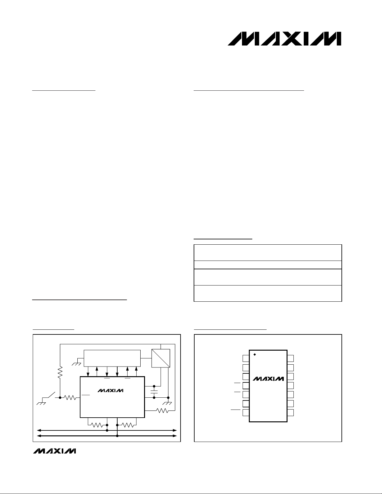
TXD RXD STB EN
ERR
INH
BATTERY
RTH
CANH CANL
RTL
BATT
GND
V
CC
WAKE
+5V
CAN CONTROLLER
235641
81112 9
7
10
13
14
100nF
V
BATT
+12V
MAX305_
CAN BUS
FAULT
TO ±80V
Typical Operating Circuit
19-2687; Rev 0; 11/02
For pricing, delivery, and ordering information, please contact Maxim/Dallas Direct! at
1-888-629-4642, or visit Maxim’s website at www.maxim-ic.com.
PART TEMP RANGE DATA RATE
MAX3054ASD -40°C to +125°C 250kbps 14 SO
MAX3055ASD -40°C to +125°C
MAX3056ASD -40°C to +125°C
Slew control
125kbps
Slew control
40kbps
PINPACKAGE
14 SO
14 SO
TOP VIEW
1
INH
2
TXD
3
RXD
4
STB
5
EN
6
7
14
BATT
13
GND
12
CANL
11
MAX3054
MAX3055
MAX3056
SO
CANHERR
V
10
CC
9
RTL
RTHWAKE
8
Page 2

MAX3054/MAX3055/MAX3056
±80V Fault-Protected/Tolerant CAN
Transceivers for In-Car Applications
2 _______________________________________________________________________________________
ABSOLUTE MAXIMUM RATINGS
DC ELECTRICAL CHARACTERISTICS
(VCC= 5V ±5%, V
BATT
= +5V to +42V, TA= T
MIN
to T
MAX
, unless otherwise noted. Typical values are at VCC= 5V, V
BATT
= 14V, R1 = 100Ω
(Figure 2), T
A
= +25°C.) (Notes 1, 2)
Stresses beyond those listed under “Absolute Maximum Ratings” may cause permanent damage to the device. These are stress ratings only, and functional
operation of the device at these or any other conditions beyond those indicated in the operational sections of the specifications is not implied. Exposure to
absolute maximum rating conditions for extended periods may affect device reliability.
(All voltages are referenced to GND)
Supply Voltage (V
CC
) ...............................................-0.3V to +6V
Battery Voltage (V
BATT
)..........................................-0.3V to +80V
TXD, RXD, ERR, STB, EN ...........................-0.3V to (V
CC
+ 0.3V)
CANH, CANL ..........................................................-80V to +80V
RTH, RTL ................................................................-0.3V to +80V
RTH, RTL Current ...........................................................±180mA
WAKE .....................................................................-0.3V to +80V
INH ..........................................................-0.3V to (V
BATT
+ 0.3V)
INH Current.......................................................................-0.5mA
Transient Voltage (ISO 7637)................................-200V, +200V*
Continuous Power Dissipation (T
A
= +70°C)
14-Pin SO (derate 8.3mW/°C above +70°C)................667mW
Operating Temperature Range .........................-40°C to +125°C
Junction Temperature......................................................+150°C
Storage Temperature Range .............................-65°C to +150°C
Lead Temperature (soldering, 10s) .................................+300°C
*Pending completion of testing.
)
)
PARAMETER SYMBOL CONDITIONS MIN TYP MAX UNITS
VOLTAGE SUPPLIES
Supply Current I
Battery Current I
Battery Power on Flag Threshold V
STB, EN, AND TXD
High-Level Input Voltage V
Low-Level Input Voltage V
High-Level Input Current I
Low-Level Input Current I
Supply Voltage—Forced
Standby Mode (Fail-Safe)
RXD AND ERR
High-Level Output Voltage V
Low-Level Output Voltage V
WAKE
Wake-Up Threshold Voltage V
Low-Level Input Current I
CC
BATT
PWRON
IH
IL
IH
IL
V
FS
OH
OL
TH(WAKE
IL(WAKE
Dominant normal operating mode, no load,
TXD = 0
Recessive normal operating mode,
TXD = V
CC
Low - p ow er m od es: V
Low-power modes at V
= V
V
BATT
WAKE
Low-power modes 1.0 3.5 V
VIN = 4V
VIN = 1V
V
= 14V 2.75 4.50 V
BATT
I
= -1mA VCC - 0.5 V
OUT
I
= 7.5mA 0 0.9 V
OUT
V
= 0V 2.0 2.7 3.4 V
STB
V
= 0V -10 -4 -1 µA
WAKE
16 30
410
= V
, V
= 14V 3 10 µA
B AT T
,
BATT
5 54 125 µA
= V
INH
T X D
C C
= V
TRL
= 5V to 27V
2.4 V
0.8 V
STB and EN 9 20
TXD -200 -80 -25
STB and EN 4 8
TXD -800 -320 -100
CC
mA
µA
µA
V
Page 3
MAX3054/MAX3055/MAX3056
±80V Fault-Protected/Tolerant CAN
Transceivers for In-Car Applications
_______________________________________________________________________________________ 3
DC ELECTRICAL CHARACTERISTICS (continued)
(VCC= 5V ±5%, V
BATT
= +5V to +42V, TA= T
MIN
to T
MAX
, unless otherwise noted. Typical values are at VCC= 5V, V
BATT
= 14V, R1 = 100Ω
(Figure 2), T
A
= +25°C.) (Notes 1, 2)
)
)
)
)
)
)
)
)
)
PARAMETER SYMBOL CONDITIONS MIN TYP MAX UNITS
INH
High-Level Voltage Drop ∆V
Leakage Current I
CANH, CANL
Differential Receiver Threshold V
Differential Receiver Hysteresis HYST No failures and bus failures 1, 2, 5, 9 18 mV
CANH Recessive Output Voltage V
CANL Recessive Output Voltage V
CANH Dominant Output Voltage V
CANL Dominant Output Voltage V
CANH Output Current I
CANL Output Current I
Voltage Detection Threshold for
Short Circuit to Battery on CANH
Voltage Detection Threshold for
Short Circuit to GND on CANL
Voltage Detection Threshold for
Short Circuit to Battery on CANL
CANL Wake-Up Threshold V
CANH Wake-Up Threshold V
CANH Single-Ended Receiver
Threshold (Failures 4, 6, 7)
CANH Single-Ended Receiver
Hysteresis
LEAK(INH
DIFF
OCH
OCL
OCHDOM
OCLDOM
O(CANH
O(CANL
V
DET(CANH
V
DTG(CANL
V
DET(CANL
THL(WAKE
THH(WAKE
V
SE(CANH
H
INH = -0.18mA, standby mode 0.8 V
Sleep mode, V
VCC = 5V, no failures and bus failures 1, 2,
5, 9
VCC = 4.75V to 5.25V, no failures and bus
failures 1, 2, 5, 9
= 0V 5 µA
INH
-3.5 -3.2 -2.9
✕ V
- 0.70
C C
TXD = VCC, RTH < 4kΩ 200 mV
TXD = VCC, RTH < 4kΩ VCC - 0.2 V
TXD = 0V, R1 = 100Ω VCC - 1.4 V
TXD = 0V, R1 = 100Ω 1.4 V
V
= 0V, TXD = 0V -150 -86 mA
CANH
Low-power modes, V
V
= 14V, TXD = 0V 75 130 mA
CANL
Low-power modes, V
V
= 42V, RTL = open
BATT
= 0V, VCC = 5V -10 µA
CANH
= 42V,
CANL
VCC = 4.75V to 5.25V 0.30 ✕ VCC 0.37 ✕ V
Low-power modes 1.1 2.5
Low-power modes 2.5 3.9 V
Normal mode, VCC = 5V 6.4 7.3 8.2 V
Low-power modes 2.5 3.2 3.9 V
Low-power modes 1.1 1.8 2.5 V
V
= 5V 1.50 1.70 1.85
CC
VCC = 4.75V to 5.25V 0.30 ✕ VCC 0.37 ✕ V
- 0.58 ✕ V
C C
20 µA
CC
CC
HYST 10 mV
V
V
V
Page 4
MAX3054/MAX3055/MAX3056
±80V Fault-Protected/Tolerant CAN
Transceivers for In-Car Applications
4 _______________________________________________________________________________________
DC ELECTRICAL CHARACTERISTICS (continued)
(VCC= 5V ±5%, V
BATT
= +5V to +42V, TA= T
MIN
to T
MAX
, unless otherwise noted. Typical values are at VCC= 5V, V
BATT
= 14V, R1 = 100Ω
(Figure 2), T
A
= +25°C.) (Notes 1, 2)
)
)
)
)
)
)
AC ELECTRICAL CHARACTERISTICS
(VCC= 5V ±5%, V
BATT
= +5V to +42V, TA= T
MIN
to T
MAX
, unless otherwise noted. Typical values are at VCC= 5V, V
BATT
= 14V, R1 = 100Ω
(Figure 2), T
A
= +25°C.) (Notes 1, 2)
CANL Single-Ended Receiver
Threshold
CANL Single-Ended Receiver
Hysteresis
RTL AND RTH
RTL to VCC Switch
On-Resistance
RTH to VCC Switch
On-Resistance
Output Current on Pin RTL I
RTL Pullup Current |I
RTH Pulldown |I
THERMAL SHUTDOWN
Shutdown Junction Temperature
Thermal Protection Hysteresis T
PARAMETER SYMBOL CONDITIONS MIN TYP MAX UNITS
V
SE(CANL
HYST Failures 3, 8 10 mV
R
SW(RTL
R
SW(RTH
O(RTL
| Normal and failures 4, 6, 7, RTL = 0V 20 107 200 µA
PU(RTL
| Normal and failures 3, 8, RTL = V
PU(RTH
T
J
T
JF6
HYS
VCC = 5V 3.15 3.30 3.45
VCC = 4.75V to 5.25V 0.63 ✕ VCC 0.69 ✕ V
IO = -10mA 36 100 Ω
IO = 10mA 23 100 Ω
Low-power modes, V
For shutdown 165
During failure 6—switch off CANL only 140
= 0 -1.25 -0.65 -0.30 mA
RTL
CC
CC
20 106 200 µA
°C
15 °C
V
TRANSITION TIME
CANL and CANH Bus Output
Transition Time Recessive to
Dominant (10% to 90%)
CANL and CANH Bus Output
Transition Time Dominant to
Recessive (10% to 90%)
PROPAGATION DELAY TXD TO RXD LOW—DOMINANT TRANSMISSION (Figures 1, 2)
Differential Reception t
PARAMETER SYMBOL CONDITIONS MIN TYP MAX UNITS
t
(r-d)
t
(d-r)
PDLD
CL = 330pF, MAX3054 (250kbps) 38
CL = 220pF to 3.3nF, MAX3055 (125kbps) 100 700
CL = 560pF to 10nF, MAX3056 (40kbps) 0.7 3.3 µs
CL = 330pF, MAX3054 (250kbps) 130
CL = 220pF to 1nF, MAX3055 (125kbps) 200 1200
CL = 560pF to 3.3nF, MAX3056 (40kbps) 0.5 2.8 µs
No failures, CL = 330pF, MAX3054
(250kbps)
Bus failures 1, 2, 5, 9,
= 330pF, MAX3054 (250kbps)
C
L
No failures and bus failures 1, 2, 5, 9,
= 1nF, MAX3055 (125kbps)
C
L
No failures and bus failures 1, 2, 5, 9,
= 3.3nF, MAX3056 (40kbps)
C
L
600
750
1.5
4.7
ns
ns
ns
µs
Page 5
MAX3054/MAX3055/MAX3056
±80V Fault-Protected/Tolerant CAN
Transceivers for In-Car Applications
_______________________________________________________________________________________ 5
AC ELECTRICAL CHARACTERISTICS (continued)
(VCC= 5V ±5%, V
BATT
= +5V to +42V, TA= T
MIN
to T
MAX
, unless otherwise noted. Typical values are at VCC= 5V, V
BATT
= 14V, R1 = 100Ω
(Figure 2), T
A
= +25°C.) (Notes 1, 2)
Single-Ended Reception t
PROPAGATION DELAY TXD TO RXD HIGH—RECESSIVE TRANSMISSION (Figures 1, 2)
Differential Reception t
Single-Ended Reception t
WAKE-UP TIMING
PARAMETER SYM B O L CONDITIONS MIN TYP MAX UNITS
PDLSE
PDHD
PDHSE
Bus failures 3, 4, 6, 7, 8,
C
= 330pF, MAX3054 (250kbps)
L
Bus failures 3, 4, 6, 7, 8,
C
= 1nF, MAX3055 (125kbps)
L
Bus failures 3, 4, 6, 7, 8,
C
= 3.3nF, MAX3056 (40kbps)
L
No failures and bus failures 1, 2, 5, 9,
= 330pF, MAX3054 (250kbps)
C
L
No failures and bus failures 1, 2, 5, 9,
= 1nF, MAX3055 (125kbps)
C
L
No failures and bus failures 1, 2, 5, 9,
C
= 3.3nF, MAX3056 (40kbps)
L
Bus failures 3, 4, 6, 7, 8,
C
= 330pF, MAX3054 (250kbps)
L
Bus failures 3, 4, 6, 7, 8,
C
= 1nF, MAX3055 (125kbps)
L
Bus failures 3, 4, 6, 7, 8,
C
= 3.3nF, MAX3056 (40kbps)
L
750 ns
1. 5
4.7
950 ns
1.9
5.95
950 ns
1.9
5.95
µs
µs
µs
Minimum Time for Wake-Up on
CANL and CANH or WAKE
FAILURES TIMING
Failures 3 and 8 Detection Time
Failures 4 and 7 Detection Time
Failure 6 Detection Time
t
WAKE
t
DET
Normal and
low-power mode
Normal and
low-power mode
Normal mode
838µs
MAX3054 (250kbps),
MAX3055 (125kbps)
MAX3056 (40kbps) 5.5 16.5 27.0
MAX3054 (250kbps),
MAX3055 (125kbps)
MAX3056 (40kbps) 1.0 3.2 5.5
MAX3054 (250kbps),
MAX3055 (125kbps)
MAX3056 (40kbps) 0.93 2.97 5.00
1.9 5.7 9.5
0.3 1 1.9
0.35 1.1 1.85
ms
Page 6
MAX3054/MAX3055/MAX3056
±80V Fault-Protected/Tolerant CAN
Transceivers for In-Car Applications
6 _______________________________________________________________________________________
AC ELECTRICAL CHARACTERISTICS (continued)
(VCC= 5V ±5%, V
BATT
= +5V to +42V, TA= T
MIN
to T
MAX
, unless otherwise noted. Typical values are at VCC= 5V, V
BATT
= 14V, R1 = 100Ω
(Figure 2), T
A
= +25°C.) (Notes 1, 2)
)
Note 1: All currents into the device are positive; all currents out of the device are negative. All voltages are referenced to device
ground, unless otherwise noted.
Note 2: Failure modes 1 through 9 are explained in Table 1 and in the Detailed Description section.
Failures 3 and 8 Recovery Time
Failures 4 and 7 Recovery Time
Failure 6 Recovery Time
Minimum Hold Time of
Go-to-Sleep Command
Disable Time of TXD Permanent
Dominant Timer
Pulse Count Difference for
Failures 1, 2, 5, 9 Detection (ERR
Becomes Low)
Pulse Count Difference for
Failures 1, 2, 5, 9 Recovery (ERR
Becomes High)
PARAMETER SYM B O L CONDITIONS MIN TYP MAX UNITS
t
REC
t
HMIN
t
DIS(TXD
Count
Normal and
low-power mode
Normal mode
Low-power mode
Normal mode
V
TXD
MAX3054 (250kbps),
MAX3055 (125kbps)
MAX3056 (40kbps) 1.0 3.2 5.5
MAX3054 (250kbps) 1.7 5.6 9.5
MAX3055 (125kbps) 7 23 38
MAX3056 (40kbps) 22 70 119
MAX3054 (250kbps),
MAX3055 (125kbps)
MAX3056 (40kbps) 1.0 3.2 5.5
MAX3054 (250kbps),
MAX3055 (125kbps)
MAX3056 (40kbps) 390 1445 2500
MAX3054 (250kbps),
= 0
MAX3055 (125kbps)
MAX3056 (40kbps) 2.34 12.50
0.36 1.14 1.90
0.35 1.1 1.85
150 525 900
550µs
0.9 4.5
4
34 5
ms
µs
ms
µs
ms
Page 7

MAX3054/MAX3055/MAX3056
±80V Fault-Protected/Tolerant CAN
Transceivers for In-Car Applications
_______________________________________________________________________________________ 7
Figure 2. Test Circuit for Dynamic Characteristics
Figure 1. Timing Diagram for Dynamic Characteristics
Figure 3. Test Circuit for Typical Operating Characteristics
Figure 4. Test Circuit for Automotive Transients
Timing Diagram/Test Circuits
V
TXD
V
CANL
V
CANH
V
DIFF
V
RXD
V
= CANH - CANL
DIFF
t
PDL
t
PDH
+5V
V
CC
GND
5V
3.6V
1.4V
0
2.2V
-3.2V
-5V
VCC/2
+5V
10 6 5
V
EN STB
CC
7
WAKE
2
TXD
MAX305_
1
INH
14
BATT
ERR GND RXD
4133
PROBE CAP INCLUDED
C
BYPASS
V
BATT
+5V
RTH
CANL
CANH
RTL
C
= 15pF
X
8
12
11
9
CL
R1
CL
R1
10 6 5
EN STB
V
C
BYPASS
+12V
CC
7
WAKE
2
TXD
MAX305_
1
INH
14
BATT
ERR GND RXD
4133
125Ω
8
RTH
511Ω
12
CANL
11
CANH
511Ω
9
RTL
125Ω
= 15pF
C
X
PROBE CAP INCLUDED
CL
CL
10 6 5
EN STB
V
+12V
C
BYPASS
CC
7
WAKE
2
TXD
MAX305_
1
INH
14
BATT
ERR GND RXD
4133
PROBE CAP INCLUDED
RTH
CANL
CANH
RTL
C
X
= 15pF
8
511Ω
12
11
9
125Ω
511Ω
125Ω
1nF
1nF
GENERATOR
1nF
1nF
Page 8

MAX3054/MAX3055/MAX3056
±80V Fault-Protected/Tolerant CAN
Transceivers for In-Car Applications
8 _______________________________________________________________________________________
Typical Operating Characteristics
(VCC= 5V, V
BATT
= +12V, RTL = RTH = 511Ω, R1 = 125Ω, and TA= +25°C; see Figure 3.)
SLEW RATE vs. TEMPERATURE
RECESSIVE TO DOMINANT
MAX3054/MAX3055/MAX3056 toc01
TEMPERATURE (°C)
SLEW RATE (V/µs)
9259-7 26
5
10
15
20
0
-40 125
MAX3055
MAX3056
MAX3054
SUPPLY CURRENT vs. DATA RATE
MAX3054/MAX3055/MAX3056 toc02
DATA RATE (kbps)
SUPPLY CURRENT (mA)
45040035030025020015010050
33
34
35
36
37
32
0 500
TA = +125°C
TA = +25°C
TA = -40°C
MAX3055
SUPPLY CURRENT vs. DATA RATE
MAX3054/MAX3055/MAX3056 toc03
DATA RATE (kbps)
SUPPLY CURRENT (mA)
1007550250 125
TA = +125°C
TA = -40°C
33
34
35
36
37
32
TA = +25°C
MAX3056
SUPPLY CURRENT vs. DATA RATE
MAX3054/MAX3055/MAX3056 toc04
DATA RATE (kbps)
SUPPLY CURRENT (mA)
302010
34
35
36
37
38
33
040
TA = +125°C
TA = +25°C
TA = -40°C
MAX3054 RECEIVER PROPAGATION
DELAY vs. TEMPERATURE
MAX3054/MAX3055/MAX3056 toc05
TEMPERATURE (°C)
RECEIVER PROPAGATION DELAY (ns)
905520-15
250
300
350
400
450
200
-50 125
RECESSIVE
CL = 330pF
DOMINANT
MAX3055 RECEIVER PROPAGATION
DELAY vs. TEMPERATURE
MAX3054/MAX3055/MAX3056 toc06
TEMPERATURE (°C)
RECEIVER PROPAGATION DELAY (ns)
905520-15
300
400
500
600
200
-50 125
RECESSIVE
DOMINANT
CL = 1nF
MAX3056 RECEIVER PROPAGATION
DELAY vs. TEMPERATURE
MAX3054/MAX3055/MAX3056 toc07
TEMPERATURE (°C)
RECEIVER PROPAGATION DELAY (µs)
905520-15
0.5
1.0
1.5
2.0
0
-50 125
RECESSIVE
DOMINANT
CL = 3.3nF
MAX3054 DRIVER PROPAGATION
DELAY vs. TEMPERATURE
MAX3054/MAX3055/MAX3056 toc08
TEMPERATURE (°C)
RECEIVER PROPAGATION DELAY (ns)
905520-15
125
150
175
200
100
-50 125
RECESSIVE
DOMINANT
CL = 330pF
MAX3055 DRIVER PROPAGATION
DELAY vs. TEMPERATURE
MAX3054/MAX3055/MAX3056 toc09
TEMPERATURE (°C)
DRIVER PROPAGATION DELAY (µs)
905520-15-50 125
CL = 1nF
RECESSIVE
DOMINANT
400
500
600
700
300
Page 9

MAX3054/MAX3055/MAX3056
±80V Fault-Protected/Tolerant CAN
Transceivers for In-Car Applications
_______________________________________________________________________________________ 9
Typical Operating Characteristics (continued)
(VCC= 5V, V
BATT
= +12V, RTL = RTH = 511Ω, R1 = 125Ω, and TA= +25°C; see Figure 3.)
MAX3056
RECEIVER PROPAGATION DELAY
MAX3054/MAX3055/MAX3056 toc16
1µs/div
DIFFERENTIAL
INPUT
5V/div
RXD
5V/div
MAX3056 DRIVER PROPAGATION
3.5
CL = 3.3nF
3.0
2.5
2.0
DRIVER PROPAGATION DELAY (µs)
1.5
DELAY vs. TEMPERATURE
RECESSIVE
DOMINANT
905520-15-50 125
TEMPERATURE (°C)
DIFFERENTIAL VOLTAGE
vs. LOAD RESISTANCE
5
4
3
2
DIFFERENTIAL VOLTAGE (V)
1
TA = +25°C
MAX3054/MAX3055/MAX3056 toc10
VOLTAGE RXD (V)
TA = +125°C
TA = -40°C
3.0
2.5
2.0
1.5
1.0
0.5
0
RECEIVER OUTPUT LOW
vs. OUTPUT CURRENT
TA = +125°C
TA = +25°C
TA = -40°C
030
OUTPUT CURRENT (mA)
RECEIVER PROPAGATION DELAY
MAX3054/MAX3055/MAX3056 toc13
252015105
3.0
2.4
1.8
MAX3054/MAX3055/MAX3056 toc11
1.2
VOLTAGE RXD (V)
0.6
0
MAX3054
MAX3054/MAX3055/MAX3056 toc14
RECEIVER OUTPUT HIGH
vs. OUTPUT CURRENT
TA = +125°C
MAX3054/MAX3055/MAX3056 toc12
TA = +25°C
TA = -40°C
018
OUTPUT CURRENT (mA)
DIFFERENTIAL
INPUT
5V/div
RXD
5V/div
1512963
0
0 500
LOAD RESISTANCE (Ω)
400300200100
200ns/div
MAX3055
RECEIVER PROPAGATION DELAY
MAX3054/MAX3055/MAX3056 toc15
400ns/div
DIFFERENTIAL
INPUT
5V/div
RXD
5V/div
Page 10

MAX3054/MAX3055/MAX3056
±80V Fault-Protected/Tolerant CAN
Transceivers for In-Car Applications
10 ______________________________________________________________________________________
Typical Operating Characteristics (continued)
(VCC= 5V, V
BATT
= +12V, RTL = RTH = 511Ω, R1 = 125Ω, and TA= +25°C; see Figure 3.)
DRIVER PROPAGATION DELAY
RECESSIVE TO DOMINANT
MAX3054/MAX3055/MAX3056 toc17
1µs/div
TXD
5V/div
MAX3054
MAX3055
MAX3056
DRIVER PROPAGATION DELAY
DOMINANT TO RECESSIVE
MAX3054/MAX3055/MAX3056 toc18
1µs/div
TXD
5V/div
MAX3056
MAX3055
MAX3054
TXD-TO-RXD PROPAGATION DELAY
DOMINANT TO RECESSIVE
MAX3054/MAX3055/MAX3056 toc19
1µs/div
TXD
MAX3056
MAX3055
MAX3054
TXD-TO-RXD PROPAGATION DELAY
RECESSIVE TO DOMINANT
MAX3054/MAX3055/MAX3056 toc20
1µs/div
TXD
MAX3054
MAX3055
MAX3056
MAX3056 CAN BUS AT 40kbps
MAX3054/MAX3055/MAX3056 toc21
4µs/div
CANH - CANL
5V/div
FFT
1V/div
MAX3054 CAN BUS AT 250kbps
MAX3054/MAX3055/MAX3056 toc23
400ns/div
CANH - CANL
10V/div
FFT
1V/div
MAX3055 CAN BUS AT 125kbps
MAX3054/MAX3055/MAX3056 toc22
2µs/div
CANH - CANL
5V/div
FFT
1V/div
Page 11

Detailed Description
The MAX3054/MAX3055/MAX3056 interface between
the protocol controller and the physical wires of the bus
lines in a CAN. The devices provide differential transmit
capability and switch to single-wire mode if certain fault
conditions occur (see the Failure Management section).
The MAX3054/MAX3055/MAX3056 guarantee full wakeup capability during failure modes.
The extended fault-protection range of CANH and
CANL bus lines (±80V) allows for use in 42V automotive
applications. A current-limiting circuit protects the
transmitter output stage against overcurrent faults. This
feature prevents destruction of the transmitter output
stage. If the junction temperature exceeds a value of
approximately +165°C, the transmitter output stages
are disabled. The CANH and CANL lines are also protected against electrical transients, which can occur in
an automotive environment.
The transceiver provides three low-power modes that
can be entered and exited through pins STB and EN.
An output INH pin can be used for deactivation of an
external voltage regulator.
The MAX3054/MAX3055/MAX3056 are designed to
provide optimal operation for a specified data rate. The
MAX3054 is ideal for high data rates of 250kbps. The
MAX3055 is used for data rates of 125kbps, and the
MAX3056 is designed for 40kbps applications. For the
40kbps and 125kbps versions, the built-in slope-control
feature allows the use of unshielded cables and receiver
input filters guarantee high noise immunity.
Normal Operation Mode
Transmitter
The transmitter converts a single-ended input (TXD)
from the CAN controller to differential outputs for the
bus lines (CANH, CANL).
Receiver
The receiver takes differential input from the bus lines
(CANH, CANL) and converts this data as a singleended output (RXD) to the CAN controller. It consists of
a comparator that senses the difference ∆V = (CANH CANL) with respect to an internal threshold.
BATT
The main function of BATT is to supply power to the
device when vehicle battery voltage is supplied.
BATT can handle up to +80V making it ideal for 42V
automotive systems allowing power-up of the device
when the ignition is turned on.
MAX3054/MAX3055/MAX3056
±80V Fault-Protected/Tolerant CAN
Transceivers for In-Car Applications
______________________________________________________________________________________ 11
Pin Description
PIN NAME FUNCTION
1 INH Inhibit Output. Inhibit output is for switching an external voltage regulator if a wake-up signal occurs.
2 TXD Transmit Data Input
3 RXD Receive Data Output
4 ERR
5 STB
6EN
7 WAKE Wake-Up. Local wake-up signal input; falling and rising edges are both detected.
8 RTH Termination Resistor. Termination resistor connection for CANH bus.
9 RTL Termination Resistor. Termination resistor connection for CANL bus.
10 V
11 CANH High-Level Voltage Bus Line
12 CANL Low-Level Voltage Bus Line
13 GND Ground
14 BATT Battery Supply. Bypass to ground with a 0.1µF capacitor.
CC
Error. Wake-up and power-on indication output; active low in normal operating mode when the bus
has a failure and in low-power modes (wake-up signal or power-on standby).
Standby. The digital control signal input (active low) defines, together with input signal on pin EN, the
state of the transceiver (in normal and low-power modes).
Enable. The digital control signal input defines, together with input signal on pin STB, the state of the
transceiver (in normal and low-power modes).
Supply Voltage. Bypass to ground with a 0.1µF capacitor.
Page 12

MAX3054/MAX3055/MAX3056
INH
Inhibit is an output that allows for the control of an external voltage regulator. On a wake-up request or power-up
on BATT, the transceiver sets the output INH high. This
feature enables the external voltage regulator to be shut
down during sleep mode to reduce power consumption.
INH is floating while entering the sleep mode and stays
floating during the sleep mode. If INH is left floating, it is
not set to a high level again until the following events
occur:
• Power-on (V
BATT
switching on at cold start)
• Rising or falling edge on WAKE
• Dominant signal longer than 38µs during EN or STB
at low level
The signals on STB and EN are internally set to a low
level when VCCis below a certain threshold voltage
providing fail-safe functionality.
After power-on (V
BATT
switched on) the signal on INH
becomes HIGH and an internal power-on flag is set.
This flag can be read in the power-on standby mode
through ERR (STB = 1, EN = 0) and is reset by entering
the normal operating mode.
EERRRR
ERR is a wake-up and power-on indicator, as well as an
error detector. Upon power-up, wake-up, or when a
bus failure is detected, the output signal on ERR
becomes LOW. Upon error recovery, the output signal
on ERR is set HIGH.
SSTTBB
STB is the standby digital control signal into the logic
controller. This is an active-low input that is used with
EN to define the status of the transceiver in normal and
low-power modes.
EN
EN is the enable digital control signal into the logic controller used in conjunction with STB to define the status
of the transceiver in normal and low-power modes.
WWAAKKEE
WAKE is an input to the logic controller within the
device to signal a wake-up condition. If WAKE receives
a positive or negative pulse for a period longer than
t
WAKE
, wake-up occurs.
±80V Fault-Protected/Tolerant CAN
Transceivers for In-Car Applications
12 ______________________________________________________________________________________
Figure 5. Block Diagram
BATT
INH
WAKE
TXD
STB
1
7
5
EN
6
2
4ms
WAKE-UP
STANDBY
CONTROLLER
THERMAL
SHUTDOWN
DRIVER
10
V
CC
9
RTL
11
CANH
12
CANL
8
RTH
ERR
4
FAULT DETECTION
RXD
3
RECEIVER
IPD
GND
MAX305_
FILTER
FILTER
Page 13

Driver Output Protection
Thermal Shutdown
If the junction temperature exceeds +165°C, the driver is
switched off. Thermal hysteresis is 15°C, disabling thermal shutdown once the temperature reaches +150°C.
Overcurrent Protection
A current-limiting circuit protects the transmitter output
stage against a short circuit to a positive and negative
battery voltage. Although the power dissipation increases
during this fault condition, this feature prevents destruction of the transmitter output stage.
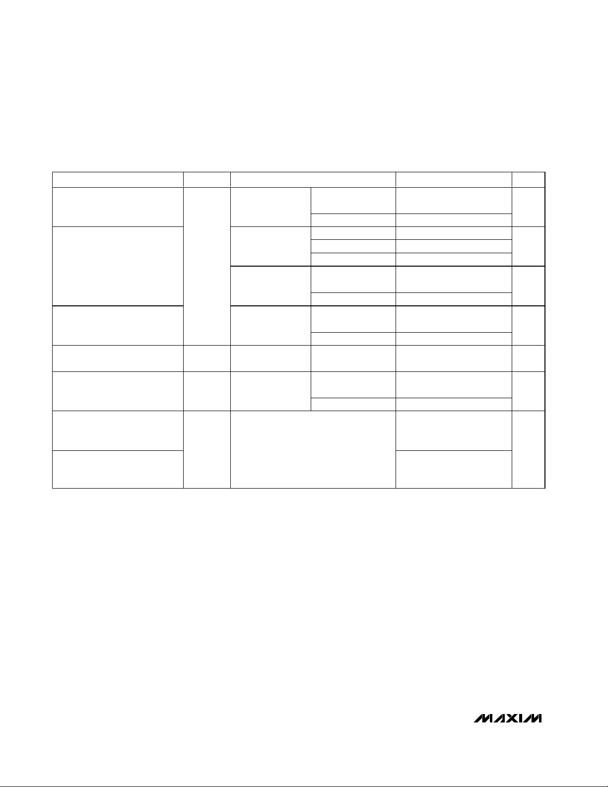
Failure Management
The failure detector is fully active in normal operating
mode. After the detection of a single failure, the detector switches to the appropriate state (see Table 1).
The differential receiver threshold voltage is set to -3.2V
typically (VCC= 5V). This ensures correct reception
with a noise margin as high as possible in the normal
operating mode and in the event of failures 1, 2, 5, and 9.
If any of the wiring failures occur, the output signal on
pin ERR becomes LOW after detection. On error recov-
ery, the output signal on pin ERR becomes HIGH.
MAX3054/MAX3055/MAX3056
±80V Fault-Protected/Tolerant CAN
Transceivers for In-Car Applications
______________________________________________________________________________________ 13
Table 1. Failure States
Failure 1—CANH Wire Interrupted (Normal Mode Only)
Failure 2—CANL Wire Interrupted (Normal Mode Only)
FAILURE DESCRIPTION MODE
1 CANH wire interrupted Normal
2 CANL wire interrupted Normal
3 CANH short circuited to battery All
4 CANL short circuited to ground All
5 CANH short circuited to ground Normal
6 CANL short circuited to battery Normal
7 CANL mutually short circuited to CANH All
8 CANH short circuited to V
9 CANL short circuited to V
CC
CC
All
Normal
MODE DESCRIPTION
The external termination resistance connected to the RTH pin provides an instantaneous pulldown of the open
Detection
Receiver The receiver remains in differential mode. No received data lost.
Driver Driver remains in differential mode. No transmission data lost.
Recovery
MODE DESCRIPTION
Detection
Receiver The receiver remains in differential mode. No received data lost.
Driver Driver remains in differential mode. No transmission data lost.
Recovery
CANH line to GND. Detection is provided, sensing the pulse-count difference between CANH and CANL (pulse
count = 4).
Recovery is provided sensing the pulse-count difference between CANH and CANL after the detection of four
consecutive pulses.
The external termination resistance connected to the RTL pin provides an instantaneous pullup of the CANL line to
. Detection is provided, sensing the pulse-count difference between CANL and CANH (pulse count = 4).
V
CC
Recovery is provided, sensing the pulse-count difference between CANL and CANH after the detection of four
consecutive pulses.
Page 14

MAX3054/MAX3055/MAX3056
±80V Fault-Protected/Tolerant CAN
Transceivers for In-Car Applications
14 ______________________________________________________________________________________
Table 1. Failure States (continued)
Failure 3—CANH Short Circuited to Battery
Failure 4—CANL Short Circuited to GND
Failure 5—CANH Short Circuited to Ground or Below Ground (Normal Mode Only)
Failure 6—CANL Short Circuited to Battery (Normal Mode Only)
Failure 7—CANL Mutually Short Circuited to CANH
MODE DESCRIPTION
Detection Sensing a permanent dominant condition on CANH for a timeout period.
Receiver Receiver switches to single ended on CANL.
Driver CANH and RTH are both switched off (high impedance) and transmission continues on CANL after timeout.
Recovery
MODE DESCRIPTION
Detection Sensing a permanent dominant condition for a timeout period.
Receiver Receiver switches to single ended on CANH.
Driver CANL and RTL are both switched off (high impedance) and transmission continues on CANH after timeout.
Recovery
MODE DESCRIPTION
Detection Detection is provided, sensing the pulse-count difference between CANH and CANL (pulse count = 4).
Receiver Receiver remains in differential mode. No received data lost.
Driver RTH remains on and CANH remains enabled.
Recovery
When the short is removed, the recessive bus voltage is restored. If the differential voltage remains below the
recessive threshold level for the timeout period, reception and transmission switch back to the differential mode.
When the short is removed, the recessive bus voltage is restored. If the differential voltage remains below the
recessive threshold level for the timeout period, reception and transmission switch back to the differential mode.
Recovery is provided, sensing the edge-count difference between CANH and CANL after the detection of four
consecutive pulses.
MODE DESCRIPTION
Detection Detected by a comparator for CANL > 7.3V after a timeout period.
Receiver Receiver switches to single ended on CANH after timeout.
Driver RTL is switched off after timeout. CANH remains active.
Recovery Sensing CANL < 7.3V after the timeout period.
MODE DESCRIPTION
Detection
Receiver Receiver switches to CANH single-ended mode after timeout.
Driver CANL and RTL are both switched off after timeout. Transmission remains ongoing on CANH.
Recovery
Sensing a permanent dominant condition on the differential comparator (CANH - CANL > -3.2V) for the timeout
period.
When the short is removed, the recessive bus voltage is restored (RTL on if CANH - CANL < -3.2V) but CANL still
remains disabled and ERR = 0. If the differential voltage remains below the recessive threshold level (CANH CANL < -3.2V) for the timeout period, reception and transmission switch back to the differential mode.
Page 15
±80V Fault-Protected/Tolerant CAN
Transceivers for In-Car Applications
Table 1. Failure States (continued)
Failure 8—CANH Short Circuited to V
cc
MAX3054/MAX3055/MAX3056
______________________________________________________________________________________ 15
Failure 9—CANL Short Circuited to Vcc(Normal Mode Only)
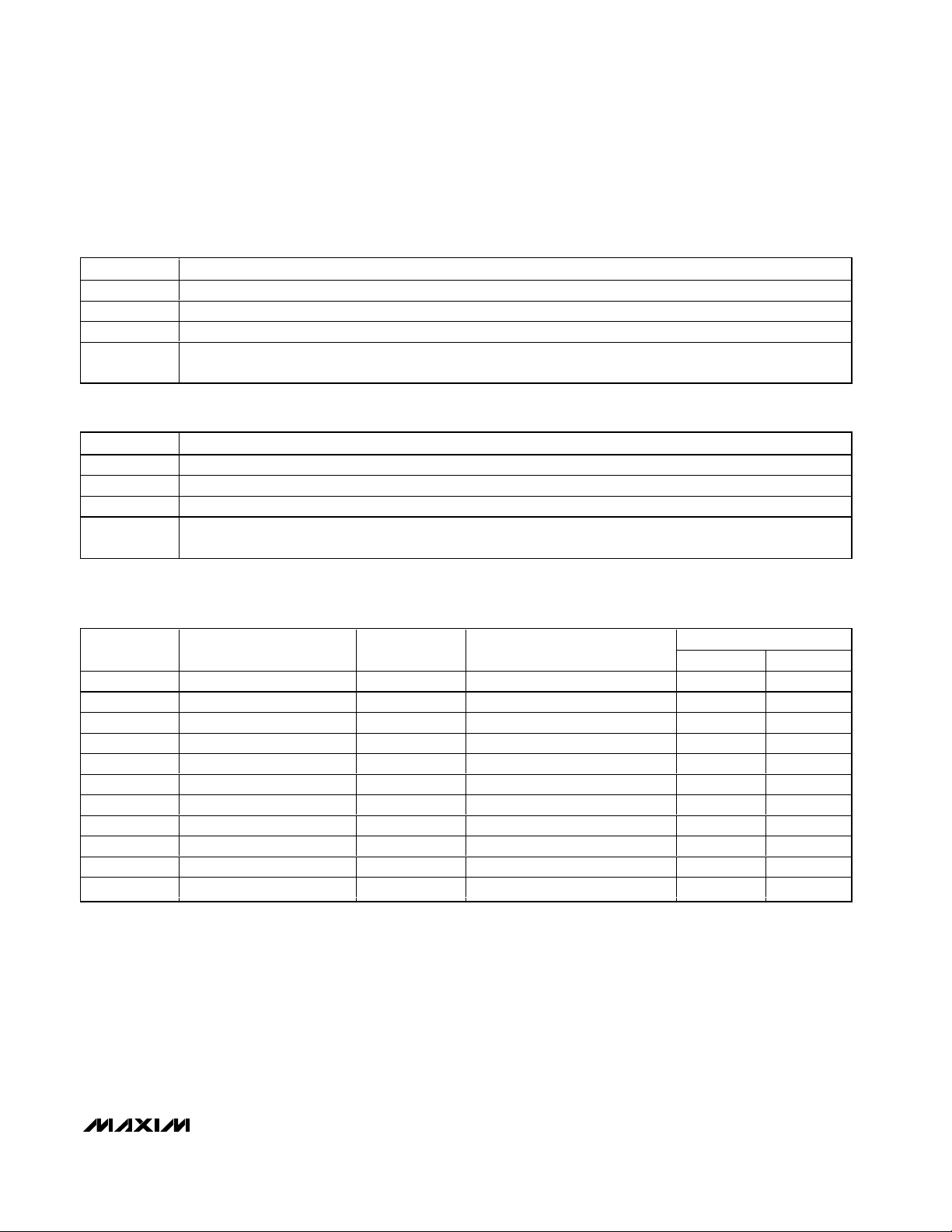
Table 2. Summary of the Driver Outputs and Internal Switches State During Fault
Conditions
Note: The RTH-pulldown current switch and the RTL-pullup current switch are closed in normal mode with or without fault conditions,
open in sleep mode.
MODE DESCRIPTION
Detection Sensing a permanent dominant condition on CANH for a timeout period.
Receiver Receiver switches to single ended on CANL.
Driver CANH and RTH are both switched off (high impedance) and transmission continues on CANL after timeout.
Recovery
MODE DESCRIPTION
Detection Detection is provided, sensing the pulse-count difference between CANL and CANH (pulse count = 4).
Receiver Receiver remains in differential mode. No received data lost.
Driver Driver remains in differential mode. No transmission data lost.
Recovery
When the short is removed, the recessive bus voltage is restored. If the differential voltage remains below the
recessive threshold level for the timeout period, reception and transmission switch back to the differential mode.
Recovery is provided, sensing the pulse-count difference between CANL and CANH after the detection of four
consecutive pulses.
FAILURE NO. DESCRIPTION MODE INTERNAL SWITCHES STATE
No failure — Normal RTH, RTL on Enabled Enabled
No failure — Low power RTH, I_RTL on Disabled Disabled
1 CANH wire interrupted Normal RTH, RTL on Enabled Enabled
2 CANL wire interrupted Normal RTH, RTL on Enabled Enabled
3 CANH short to BATT All RTH off Disabled Enabled
4 CANL short to GND All RTL or I_RTL off Enabled Disabled
5 CANH short to GND Normal RTH, RTL on Enabled Enabled
6 CANL short to BATT Normal RTL off, RTH on Enabled Enabled
7 CANL short to CANH All RTL or I_RTL off Enabled Disabled
8 CANH short to V
9 CANL short to V
CC
CC
All RTH off Disabled Enabled
Normal RTH, RTL on Enabled Enabled
DRIVER OUTPUTS STATE
CANH CANL
Page 16

Low-Power Modes
The transceiver provides three low-power modes that can
be entered or exited through pins STB and EN (Table 3).
Sleep Mode
The sleep mode is the mode with the lowest power consumption. INH is switched to high impedance for deactivation of the external voltage regulator. CANL is biased
to the battery voltage through RTL. If the supply voltage
is provided, RXD and ERR signal the wake-up interrupt.
Standby Mode
The standby mode reacts the same as the sleep mode,
but with a HIGH level on INH. Standby mode can be
used when the external voltage regulator needs to be
kept active during low-power operation.
Power-On Standby Mode
The power-on standby mode behaves similarly to the
standby mode with the battery power-on flag of the
wake-up interrupt signal on ERR. This mode is only for
reading the power-on flag. INH can be high or low in
the power-on standby mode. When the device goes
from standby mode to power-on standby mode, INH is
HIGH. When the device goes from sleep mode to
power-on standby mode, INH is low.
Wake-Up
Wake-up requests are recognized by the transceiver
when a dominant signal is detected on either bus line
or if WAKE detects a pulse for more than 38µs. On a
wake-up request, INH is set high to activate an external
voltage regulator.
If VCCis provided, the wake-up request can be read on
the ERR or RXD outputs.
To prevent false wake-up due to transients or RF fields,
the wake-up voltage levels have to be maintained for more
than 38µs. In the low-power modes, the failure detection
circuit remains partly active to prevent increased power
consumption in the event of failures 3, 4, 7, and 8.
Applications Information
The MAX3054/MAX3055/MAX3056 are capable of sustaining a network of up to 32 transceivers on a single
bus. The fault-tolerant transceivers are designed to
operate at a total termination resistance of 100Ω. Both
CANH and CANL lines are terminated with 100Ω. Since
the total termination resistance of the system is distributed over the entire bus, each of the transceivers contributes only part of the total 100Ω termination. The
values of the termination resistors RTL and RTH vary
according to the size of the system and need to be calculated. It is not required that each transceiver be terminated with the same value, the total termination need
only be a total 100Ω.
The minimum termination resistor value allowed for
each transceiver is 500Ω, due to the driving capability
of RTH and RTL. This makes it impossible to achieve a
total termination resistance of 100Ω for systems smaller
than five transceivers. Typically this does not create a
problem because smaller systems usually have shorter
bus cables and have no problem with higher total termination resistance.
To reduce EMI in the case of an interrupted bus wire it
is recommended not to exceed 6kΩ termination resistance at a single transceiver even though a higher
value is specified.
MAX3054/MAX3055/MAX3056
±80V Fault-Protected/Tolerant CAN
Transceivers for In-Car Applications
16 ______________________________________________________________________________________
Note 1: In case the go-to-sleep command was used before.
Note 2: If the supply voltage V
CC
is present.
Note 3: Wake-up interrupts are released when entering the normal operating mode.
Table 3. Low-Power Modes
MODE STB EN
Go-to-Sleep
Command
Sleep 0 0 (Note 1)
Standby 0 0
Power-On
Standby
Normal
Operating
01
10
1 1 Error flag No error flag
LOW HIGH LOW HIGH
Wake-up
interrupt signal
(Notes 2 and 3)
V
power-on
BATT
flag
ERR RXD
Wake-up
—
—
interrupt signal
(Notes 2 and 3)
Wake-up
interrupt signal
(Notes 2 and 3)
Dominant
received data
— V
— V
Recessive
received data
RTL
SWITCHED TO
BATT
BATT
V
CC
Page 17

Reduced EMI and Reflections
Due to internal slope control for the MAX3055/
MAX3056, the CANH and CANL outputs are slew-rate
limited. This minimizes EMI and reduces reflections
caused by improperly terminated cables. In general, a
transmitter’s rise time relates directly to the length of an
unterminated stub, which can be driven with only minor
waveform reflections. The following equation expresses
this relationship conservatively:
Length = t
RISE
/ (15ns/ft)
where t
RISE
is the transmitter’s rise time.
The MAX3054/MAX3055/MAX3056 require no special
layout considerations beyond common practices.
Bypass V
CC
to GND with a 0.1µF ceramic capacitor
mounted close to the IC with short lead lengths and
wide trace widths.
Chip Information
TRANSISTOR COUNT: 1300
PROCESS: BiCMOS
MAX3054/MAX3055/MAX3056
±80V Fault-Protected/Tolerant CAN
Transceivers for In-Car Applications
______________________________________________________________________________________ 17______________________________________________________________________________________ 17
Page 18

MAX3054/MAX3055/MAX3056
±80V Fault-Protected/Tolerant CAN
Transceivers for In-Car Applications
Maxim cannot assume responsibility for use of any circuitry other than circuitry entirely embodied in a Maxim product. No circuit patent licenses are
implied. Maxim reserves the right to change the circuitry and specifications without notice at any time.
18 ____________________Maxim Integrated Products, 120 San Gabriel Drive, Sunnyvale, CA 94086 408-737-7600
© 2002 Maxim Integrated Products Printed USA is a registered trademark of Maxim Integrated Products.
Package Information
(The package drawing(s) in this data sheet may not reflect the most current specifications. For the latest package outline information,
go to www.maxim-ic.com/packages.)
14L SOIC.EPS
 Loading...