

Page 1
MAX3053
±80V Fault-Protected, 2Mbps,
Low Supply Current CAN Transceiver
________________________________________________________________ Maxim Integrated Products 1
For pricing delivery, and ordering information please contact Maxim/Dallas Direct! at
1-888-629-4642, or visit Maxim’s website at www.maxim-ic.com.
General Description
The MAX3053 interfaces between the control area network (CAN) protocol controller and the physical wires of
the bus lines in a CAN. It is primarily intended for industrial systems requiring data rates up to 2Mbps and features ±80V fault protection against shorts to
high-voltage power buses. The device provides differential transmit capability to the bus and differential
receive capability to the CAN controller.
The MAX3053 has three different modes of operation:
high-speed, slope control, and shutdown. High-speed
mode allows data rates up to 2Mbps. In slope control
mode, data rates are between 40kbps and 500kbps so
the effects of EMI are reduced and unshielded twisted
or parallel cable may be used. In shutdown mode, the
transmitter is switched off, and the receiver is switched
to a low-current mode.
An autoshutdown function puts the device in 15µA shutdown mode when the bus or CAN controller is inactive
for 47ms or greater.
The MAX3053 is available in an 8-pin SO package and
is specified for -40°C to +125°C operation.
Applications
Industrial Control and Networks
Printers
Automotive Systems
HVAC Controls
Telecom 72V Systems
Features
♦ ±80V Fault Protection
♦ Three Operating Modes
High-Speed Operation up to 2Mbps
Slope Control Mode to Reduce EMI
(40kbps to 500kbps)
♦ 15µA Low-Current Shutdown Mode
♦ Autoshutdown when Device Is Inactive
♦ Automatic Wakeup from Shutdown
♦ Thermal Shutdown
♦ Current Limiting
♦ Fully Compatible with the ISO 11898 Standard
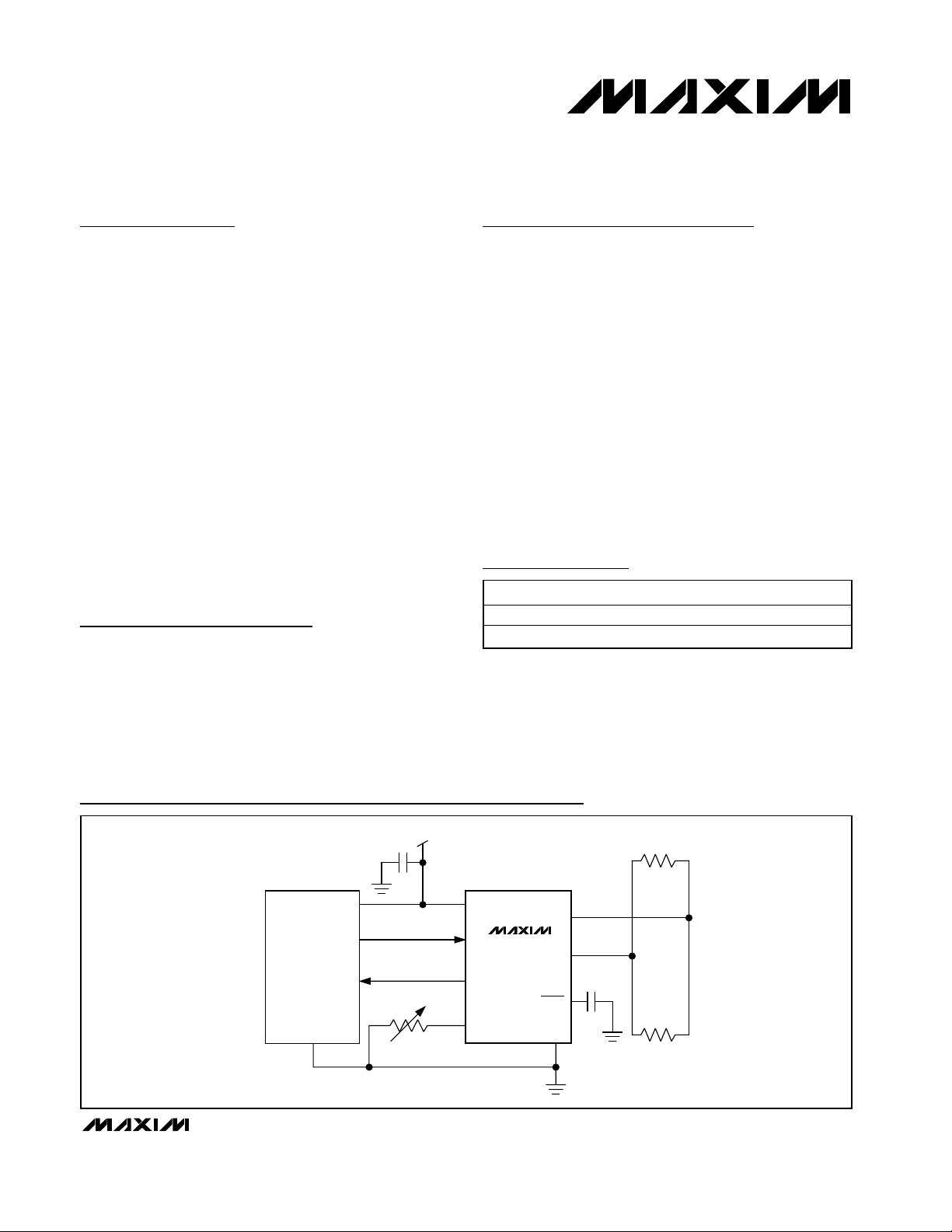
Ordering Information
TXD
RXD
RS
25kΩ TO 180kΩ
V
CC
CANL
GND
CANH
120Ω
100nF
MAX3053
SHDN
GND
TXD
100nF
CAN
CONTROLLER
V
CC
120Ω
RXD
Typical Operating Circuit
19-2425; Rev 0; 4/02
Pin Configuration appears at end of data sheet.
PART TEMP RANGE PIN-PACKAGE
MAX3053ESA -40°C to +85°C 8 SO
MAX3053ASA -40°C to +125°C 8 SO
Page 2
MAX3053
±80V Fault-Protected, 2Mbps,
Low Supply Current CAN Transceiver
2 _______________________________________________________________________________________
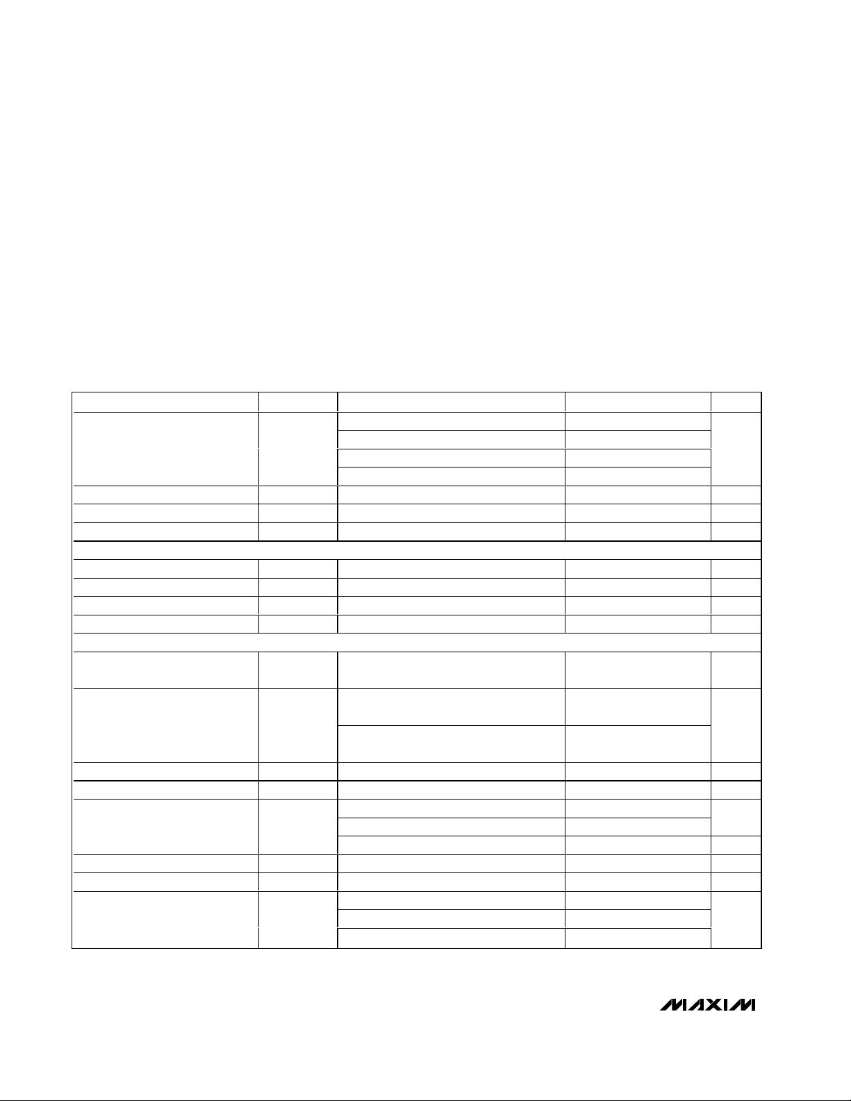
ABSOLUTE MAXIMUM RATINGS
DC ELECTRICAL CHARACTERISTICS
(VCC= +5V ±10%, RL= 60Ω, RS = GND, TA= T
MIN
to T
MAX
, unless otherwise noted. Typical values are at VCC= +5V and TA= +25°C.)
Stresses beyond those listed under “Absolute Maximum Ratings” may cause permanent damage to the device. These are stress ratings only, and functional
operation of the device at these or any other conditions beyond those indicated in the operational sections of the specifications is not implied. Exposure to
absolute maximum rating conditions for extended periods may affect device reliability.
V
CC
to GND
............................................................ -0.3V to +6V
TXD, RS, RXD, SHDN to GND ....................-0.3V to (VCC+ 0.3V)
RXD Shorted to GND................................................. Continuous
CANH, CANL to GND...........................-80V to +80V Continuous
Continuous Power Dissipation
8-Pin SO (derate 5.9mW/°C above +70°C) .................470mW
Operating Temperature Ranges
MAX3053ASA ...............................................-40°C to +125°C
MAX3053ESA .................................................-40°C to +85°C
Junction Temperature......................................................+150°C
Storage Temperature Range .............................-65°C to +150°C
Lead Temperature (soldering, 10s) ................................+300°C
Supply Current I
Shutdown Supply Current I
Thermal Shutdown Threshold 160 °C
Thermal Shutdown Hysteresis 20 °C
TXD INPUT LEVELS
High-Level Input Voltage V
Low-Level Input Voltage V
High-Level Input Current I
Pullup Resistor R
CANH, CANL TRANSMITTER
Recessive Bus Voltage
Off-State Output Leakage I
CANH Output Voltage V
CANL Output Voltage V
Differential Output
(V
CANH
CANH Short-Circuit Current I
CANL Short-Circuit Current I
ESD CANH, CANL (Note 2)
PARAMETER SYMBOL CONDITIONS MIN TYP MAX UNITS
Dominant (Note 1) 56 72
S
Dominant (no load) 6
Recessive (Note 1) 3.6 5.5
Recessive (no load) 5.5
SHDN = GND 15 30 µA
2.0 V
0.4 V
V
TXD
= V
CC
1µA
20 kΩ
V
= VCC, no load 2 3 V
TXD
-2V < V
SHDN = GND, V
-80V < V
SHDN = GND, V
V
TXD
V
TXD
V
TXD
,
V
TXD
V
TXD
V
CANH
V
CANL
, V
CANH
CANH
= 0 3.0 V
CANL
, V
TXD
CANL
TXD
< +7V,
= V
< +80V,
= V
CC
CC
-2 +1
-4 +4
CC
= 0 0 2.0 V
= 0 1.5 5
= 0, RL = 45Ω 1.5
= VCC; no load -500 +50 mV
= -5V -200 mA
= 18V 200 mA
- V
CANL
QSHDN
IH
IL
IH
INTXD
V
CANH,
V
CANL
LO
CANH
CANL
∆V
CANH
)
V
CANL
SC
SC
Human Body Model ± 2
IEC1000-4-2 Air-Gap Discharge ± 3
IEC1000-4-2 Contact Discharge ± 2.5
mA
mA
V
V
kV
Page 3

MAX3053
±80V Fault-Protected, 2Mbps,
Low Supply Current CAN Transceiver
_______________________________________________________________________________________ 3
DC ELECTRICAL CHARACTERISTICS (continued)
(VCC= +5V ±10%, RL= 60Ω, RS = GND, TA= T
MIN
to T
MAX
, unless otherwise noted. Typical values are at VCC= +5V and TA= +25°C.)
)
)
DC BUS RECEIVER (V
Differential Input Voltage
(Recessive)
Differential Input Voltage
(Dominant)
Differential Input Hysteresis V
CANH Input Wakeup Voltage
Threshold
RXD High-Level Output Voltage V
RXD Low-Level Output Voltage V
CANH and CANL Input
Resistance
Differential Input Resistance R
SLOPE CONTROL
Input Voltage for High Speed V
Slope Control Mode Voltage V
Slope Control Mode Current I
High-Speed Mode Current I
AUTOSHUTDOWN
SHDN Input Voltage High 2V
SHDN Input Voltage Low 0.5 V
PARAMETER SYMBOL CONDITIONS MIN TYP MAX UNITS
= VCC; CANH and CANL externally driven (-2V < V
TXD
V
DIFF
V
DIFF
DIFF(HYST
V
CANH(SHDN
OH
OL
R
DIFF
SLP
SLOPE
SLOPE
HS
I
, V
CANH
-7V < V
-7V < V
SHDN = GND, V
I = -100µA
I = 10mA 0.8
I = 5mA 0.4
RRS = 24kΩ to 180kΩ
RRS = 24kΩ to 180kΩ, VCC = +5.0V -10 -200 µA
V
= 0 -500 µA
RS
CANH
CANH
, V
, V
< +12V -1.0 +0.5 V
CANL
< +12V 0.9 3.3 V
CANL
= V
TXD
CC
< +7V, unless otherwise specified)
CANL
150 mV
69V
0.8 x
V
CC
525kΩ
10 100 kΩ
0.4 x
V
CC
0.3 x
V
CC
0.6 x
V
CC
V
V
V
V
Page 4
MAX3053
±80V Fault-Protected, 2Mbps,
Low Supply Current CAN Transceiver
4 _______________________________________________________________________________________
TIMING CHARACTERISTICS
(VCC= +5V ±10%, RL= 60Ω, CL= 100pF, TA= T
MIN
to T
MAX
, unless otherwise noted. Typical values are at VCC= +5V and
T
A
= +25°C.) (Figures 1, 2, and 3)
Note 1: As defined by ISOSHDN, bus value is one of two complementary logical values: dominant or recessive. The dominant value
represents the logical 1 and the recessive represents the logical 0. During the simultaneous transmission of the dominant
and recessive bits, the resulting bus value is dominant. For MAX3053 values, see the truth table in the Transmitter and
Receiver sections.
Note 2: The ESD structures do not short out CANH and CANL under an ESD event while -7V < CANH, CANL < +12V.
Minimum Bit Time t
Delay TXD to Bus Active t
Delay TXD to Bus Inactive t
Delay TXD to Receiver Active t
Delay TXD to Receiver Inactive t
Time to Wakeup: CANH > 9V t
Time to Sleep Mode when Bus Is
Recessive
PARAMETER SYMBOL CONDITIONS MIN TYP MAX UNITS
BIT
ONTXD
OFFTXD
ONRXD
OFFRXD
WAKE
t
SHDN
V
= 0 (2Mbps) 0.5
RS
RRS = 24kΩ (500kbps) 2
RRS = 100kΩ (125kbps) 8
RRS = 180kΩ (62.5kbps) 25
V
= 0 40 ns
RS
V
= 0 75 ns
RS
V
= 0 (2Mbps) 120 ns
RS
RRS = 24kΩ (500kbps) 0.4
RRS = 100kΩ (125kbps) 1.6
RRS = 180kΩ (62.5kbps) 5.0
V
= 0 (2Mbps) 130 ns
RS
RRS = 24kΩ (500kbps) 0.45
RRS = 100kΩ (125kbps) 1.6
RRS = 180kΩ (62.5kbps) 5.0
RRS = 24kΩ (500kbps) 14
RRS = 100kΩ (125kbps) 7Differential Output Slew Rate |SR|
R
= 180kΩ (62.5kbps) 1.6
RS
SHDN = GND, V
C
SHDN
= V
TXD
CC
= 100nF 10 47 ms
µs
µs
µs
V/µs
10 µs
Page 5

MAX3053
±80V Fault-Protected, 2Mbps,
Low Supply Current CAN Transceiver
_______________________________________________________________________________________ 5
Typical Operating Characteristics
(VCC= +5V, RL= 60Ω, CL= 100pF, TA= +25°C, unless otherwise specified.)
25
20
15
10
5
0
20 11065 155 200
SLEW RATE vs. R
RS
MAX3053 toc01
R
RS
(kΩ)
SLEW RATE (V/µs)
TA = -40°C
TA = +125°C
TA = +25°C
0
20
10
40
30
50
60
70
80
0 100 15050 200 250 300 350 400
AUTOSHUTDOWN vs. C
SHDN
MAX3053 toc02
C
SHDN
(nF)
SLEEP TIME (ms)
30
28
26
24
22
20
0 1000500 1500 2000
SUPPLY CURRENT vs. DATA RATE
50% DUTY CYCLE
MAX3053 toc03
DATA RATE (kbps)
SUPPLY CURRENT (mA)
TA = +125°C
TA = -40°C
TA = +25°C
40
35
30
25
20
15
-50 20-15 55 90 125
RECEIVER PROPAGATION DELAY vs.
TEMPERATURE (RECESSIVE TO DOMINANT)
MAX3053 toc04
TEMPERATURE (°C)
RECEIVER PROPAGATION DELAY (ns)
35
30
25
20
15
-40 26-7 59 92 125
DRIVER PROPAGATION DELAY
vs. TEMPERATURE, R
RS
= GND
MAX3053 toc05
TEMPERATURE (°C)
DRIVER PROPAGATION DELAY (ns)
DOMINANT
RECESSIVE
1600
1200
800
400
0
0105152025
RECEIVER OUTPUT LOW
vs. OUTPUT CURRENT
MAX3053 toc06
OUTPUT CURRENT (mA)
VOLTAGE RXD (mV)
TA = -40°C
TA = +25°C
TA = +125°C
3.0
2.4
1.8
1.2
0.6
0
0105152025
RECEIVER OUTPUT HIGH
vs. OUTPUT CURRENT
MAX3053 toc07
OUTPUT CURRENT (mA)
VOLTAGE RXD (V)
TA = -40°C
TA = +25°C
TA = +125°C
5
4
3
2
1
0
010050 150 250200 300
DIFFERENTIAL VOLTAGE (CANH - CANL)
vs. DIFFERENTIAL LOAD R
L
MAX3053 toc08
DIFFERENTIAL LOAD RL (Ω)
DIFFERENTIAL VOLTAGE (V)
TA = +25°C
TA = -40°C
TA = +125°C
RECEIVER PROPAGATION DELAY
(DOMINANT TO RECESSIVE)
MAX3053 toc09
40ns/div
DIFFERENTIAL
INPUT
2V/div
Page 6

MAX3053
±80V Fault-Protected, 2Mbps,
Low Supply Current CAN Transceiver
6 _______________________________________________________________________________________
Typical Operating Characteristics (continued)
(VCC= +5V, RL= 60Ω, CL= 100pF, TA= +25°C, unless otherwise specified.)
DRIVER PROPAGATION DELAY
MAX3053 toc11
400ns/div
TXD
CANH - CANL
R
RS
= 24kΩ
5V/div
1V/div
R
RS
= 100kΩ
R
RS
= 180kΩ
Pin Description
DRIVER PROPAGATION DELAY
TXD
MAX3053 toc10
CANH - CANL
PIN NAME FUNCTION
1 TXD Transmit Data Input. TXD is a CMOS/TTL-compatible input from a CAN controller.
2 GND Ground
3VCCSupply Voltage. Bypass V
4 RXD Receive Data Output. RXD is a CMOS/TTL-compatible output from the physical bus lines CANH and CANL.
5 SHDN
6 CANL CAN Bus Line LOW. CANL is fault protected to ±80V.
7 CANH CAN Bus Line HIGH. CANH is fault protected to ±80V.
8RS
2V/div
= GND
R
RS
40ns/div
to GND with a 0.1µF capacitor.
CC
Shutdown Input. Drive SHDN low to put the MAX3053 in shutdown mode. See the Detailed Description
section for a full explanation of SHDN behavior.
Mode Select Pin. Drive RS low or connect to GND for high-speed operation. Connect a resistor from RS to
GND to control output slope. See the Mode Selection section.
Page 7

MAX3053
±80V Fault-Protected, 2Mbps,
Low Supply Current CAN Transceiver
_______________________________________________________________________________________ 7
Figure 1. AC Test Circuit
Figure 2. Timing Diagram for Dynamic Characteristics
Figure 3. Time to Wakeup (t
wake
)
Test Circuits/Timing Diagrams
CONTROLLER
TXD
CAN
TXD
RXD
30pF
V
CC
0.1µF
24kΩ TO 180kΩ
V
TXD
RXD
RS
CC
120Ω
CANH
MAX3053
CANL
100nF
SHDN
GND
120Ω
CANH
CANL
DOMINANT
CANH–CANL
RXD
t
ONTXD
t
ONRXD
V
/2 VCC/2
CC
0.5V
0.9V
RECESSIVE
t
OFFTXD
t
OFFRXD
CANH
V
SHDN
t
WAKE
9V
V
= 2V
SHDN
Page 8

MAX3053
±80V Fault-Protected, 2Mbps,
Low Supply Current CAN Transceiver
8 _______________________________________________________________________________________
Detailed Description
The MAX3053 interfaces between the protocol controller and the physical wires of a CAN bus. It is primarily intended for industrial applications requiring data
rates up to 2Mbps and features ±80V fault protection
against shorts in high-voltage systems. This fault protection allows the device to withstand up to ±80V with
respect to ground with no damage to the device. The
built-in fault tolerance allows the device to survive in
industrial and automotive environments with no external
protection devices. The device provides differential
transmit capability to the bus and differential receive
capability to the CAN controller (Figure 4).
The device has three modes of operations: high-speed,
slope control, and shutdown. In high-speed mode, slew
rates are not limited, making 2Mbps transmission
speeds possible. Slew rates are controlled in slope
control mode, minimizing EMI and allowing use of
unshielded twisted or parallel cable. The device goes
into low-power operation in shutdown mode.
The transceiver is designed to operate from a single
+5V supply, and draws 56mA of supply current in dominant state and 3.6mA in recessive state. In shutdown
mode, supply current is reduced to 15µA.
CANH and CANL are output short circuit current limited
and are protected against excessive power dissipation
by thermal-shutdown circuitry that places the driver
outputs into a high-impedance state.
Fault Protection
The MAX3053 features ±80V fault protection. This
extended voltage range of CANH and CANL bus lines
allows its use in high-voltage systems and communicating to high-voltage buses. If data is transmitting at
2Mbps, the fault protection is reduced to ±70V.
Transmitter
The transmitter converts a single-ended input (TXD)
from the CAN controller to differential outputs for the
bus lines (CANH, CANL). Table 1 is the truth table for
the transmitter and receiver.
High Speed
Connect RS to ground to set the MAX3053 to highspeed mode. When operating in high-speed mode, the
MAX3053 can achieve transmission rates up to 2Mbps.
Line drivers are switched on and off as quickly as possible. However, in this mode, no measures are taken to
limit the rise and fall slope of the data signal, allowing
for potential EMI emissions. If using the MAX3053 in
high-speed mode, use shielded twisted-pair cable to
avoid EMI problems.
THERMAL
SHUTDOWN
CANH
V
CC
TXD
RS
RXD
CANL
GND
AUTOSHUTDOWN
TRANSMITTER
CONTROL
MODE
SELECTION
RECEIVER
WAKE
0.75V
7.5V
SHDN
MAX3053
Figure 4. Block Diagram
Page 9

MAX3053
±80V Fault-Protected, 2Mbps,
Low Supply Current CAN Transceiver
_______________________________________________________________________________________ 9
Slope Control
Connect a resistor from RS to ground to select slope control mode (see Table 2). In slope control mode, the gates
of the line drivers are charged with a controlled current,
proportional to the resistor connected to the RS pin.
Transmission speed ranges from 40kbps to 500kbps.
Controlling the rise and fall slope reduces EMI and allows
the use of an unshielded twisted pair or a parallel pair of
wires as bus lines. The transfer function for selecting the
resistor value is given by:
R
RS
(kΩ) = 12000 / speed (in kbps).
See the Typical Operating Characteristics for the Slew
Rate vs. RRSgraph.
Shutdown
To place the MAX3053 in shutdown, the SHDN pin
should be driven to GND. In shutdown mode, the
device is switched off. The outputs are high impedance
to ±80V.
Receiver
The receiver takes differential input from the bus lines
(CANH, CANL) and converts this data to a singleended output (RXD) to the CAN controller. It consists of
a comparator that senses the difference ∆V = (CANH CANL) with respect to an internal threshold of 0.7V. If
this difference is positive (i.e., ∆V > 0.9V), a logic low is
present at the RXD pin. If negative (i.e., ∆V < 0.5V), a
logic high is present.
The receiver always echoes the transmitted data.
The CANH and CANL common-mode range is from -7V
to +12V. RXD is logic high when CANH and CANL are
shorted or terminated and undriven.
Thermal Shutdown
If the junction temperature exceeds +160°C, the device
is switched off. The hysteresis is about 20°C, disabling
thermal shutdown once the temperature declines to
+140°C and the device is turned back on.
Autoshutdown
To manage power consumption, autoshutdown puts the
device into shutdown mode after the device has been
inactive for a period of time. The value of an external
capacitor (C
SHDN
) connected to SHDN determines the
threshold of inactivity time, after which the autoshutdown
triggers (see Typical Operating Characteristics).
Use a 100nF capacitor as C
SHDN
for a typical threshold
of 20ms. Change the capacitor value according to the
following equation to change the threshold time period:
Drive SHDN high to force the MAX3053 on and disable
autoshutdown.
When the MAX3053 is in shutdown mode, only the
wakeup comparator is active, and normal bus communication is ignored. The remote master of the CAN system wakes up the MAX3053 with a signal greater than
9V on CANH. The local CAN controller wakes up the
MAX3053 by driving SHDN high or TXD.
Driver Output Protection
The MAX3053 has several features to protect itself from
damage. Thermal shutdown switches off the device
and puts CANH and CANL into high impedance if the
junction temperature exceeds +160°C. Thermal protection is needed particularly when a bus line is short circuited. The hysteresis for the thermal shutdown is
about 20°C.
Table 1. Transmitter and Receiver Truth Table
Table 2. Mode Selection Truth Table
*X = Don’t care.
**As defined by ISO, bus value is one of two complementary logical values: dominant or recessive. The dominant value represents
the logical 0 and the recessive represents the logical 1. During the simultaneous transmission of the dominant and recessive bits, the
resulting bus value is dominant.
TXD SHDN CANH CANL BUS STATE RXD
0V
1 or float V
X* V
> 1.5V HIGH LOW Dominant** 0
SHDN
> 1.5V 5Ω to 25kΩ to Vcc/2 5Ω to 25kΩ to Vcc/2 Recessive** 1
SHDN
< 0.5V Floating Floating Floating 1
SHDN
CONDITION
FORCED AT PIN RS
VRS < 0.3V
0.4VCC < VRS <
0.6V
CC
CC
MODE
High speed |IRs| < 500µA
Slope control 10µA < |IRs| < 200µA
RESULTING
CURRENT AT RS
I A time ms
C
nfSHDN )
(
=
SHDN
CC
(()
µ×
)
V
SHDN
(
−(V V )
˚˚ )
Page 10

MAX3053
±80V Fault-Protected, 2Mbps,
Low Supply Current CAN Transceiver
10 ______________________________________________________________________________________
Additionally, a current-limiting circuit protects the transmitter output stage against a short circuit to positive
and negative battery voltage. Although the power dissipation increases during this fault condition, this feature
prevents destruction of the transmitter output stage.
Applications Information
Reduced EMI and Reflections
In slope control mode, the CANH, CANL outputs are
slew-rate limited, minimizing EMI and reducing reflections caused by improperly terminated cables. In general, a transmitter’s rise time relates directly to the
length of an unterminated stub, which can be driven
with only minor waveform reflections. The following
equation expresses this relationship conservatively:
Length = t
RISE
/ (10 x 1.5ns/ft)
where t
RISE
is the transmitter’s rise time. See Figures 5,
6, and 7 for typical waveforms at various data rates.
The MAX3053 requires no special layout considerations
beyond common practices. Bypass VCCto GND with a
1µF ceramic capacitor mounted close to the IC with
short lead lengths and wide trace widths.
Figure 6. Output Bus in Slope Control Mode at 500kbps
Figure 5. Output Bus in Slope Control Mode at 62.5kbps
Figure 7. Output Bus High-Speed Mode at 2Mbps
1
2
3
4
8
7
6
5
RS
CANH
CANL
SHDNRXD
V
CC
GND
TXD
MAX3053
SO
TOP VIEW
Pin Configuration
Chip Information
TRANSISTOR COUNT: 1214
PROCESS: BiCMOS
CANH–CANL
5V/div
FFT
200mV/div
31.5kHz
= 180kΩ
R
RS
4.00µs
CANH–CANL
5V/div
FFT
200mV/div
250kHz
= 24kΩ
R
RS
400ns
CANH–CANL
5V/div
FFT
200mV/div
1MHz
= 0Ω
R
RS
100ns
Page 11

MAX3053
±80V Fault-Protected, 2Mbps,
Low Supply Current CAN Transceiver
Maxim cannot assume responsibility for use of any circuitry other than circuitry entirely embodied in a Maxim product. No circuit patent licenses are
implied. Maxim reserves the right to change the circuitry and specifications without notice at any time.
Maxim Integrated Products, 120 San Gabriel Drive, Sunnyvale, CA 94086 408-737-7600 ____________________ 11
© 2002 Maxim Integrated Products Printed USA is a registered trademark of Maxim Integrated Products.
Package Information
(The package drawing(s) in this data sheet may not reflect the most current specifications. For the latest package outline information,
go to www.maxim-ic.com/packages.)
9LUCSP, 3x3.EPS
 Loading...