

General Description
The MAX3051 interfaces between the CAN protocol
controller and the physical wires of the bus lines in a
controller area network (CAN). The MAX3051 provides
differential transmit capability to the bus and differential
receive capability to the CAN controller. The MAX3051
is primarily intended for +3.3V single-supply applications that do not require the stringent fault protection
specified by the automotive industry (ISO 11898).
The MAX3051 features four different modes of operation: high-speed, slope-control, standby, and shutdown
mode. High-speed mode allows data rates up to
1Mbps. The slope-control mode can be used to
program the slew rate of the transmitter for data rates of
up to 500kbps. This reduces the effects of EMI, thus
allowing the use of unshielded twisted or parallel cable.
In standby mode, the transmitter is shut off and the
receiver is pulled high, placing the MAX3051 in lowcurrent mode. In shutdown mode, the transmitter and
receiver are switched off.
The MAX3051 input common-mode range is from -7V to
+12V, exceeding the ISO 11898 specification of -2V to
+7V. These features, and the programmable slew-rate
limiting, make the part ideal for nonautomotive, harsh
environments. The MAX3051 is available in 8-pin SO
and SOT23 packages and operates over the -40°C to
+85°C extended temperature range.
Applications
Printers JetLink
Industrial Control and Networks
Telecom Backplane
Consumer Applications
Features
♦ Low +3.3V Single-Supply Operation
♦ Wide -7V to +12V Common-Mode Range
♦ Small SOT23 Package
♦ Four Operating Modes
High-Speed Operation Up to 1Mbps
Slope-Control Mode to Reduce EMI (Up to 500kbps)
Standby Mode
Low-Current Shutdown Mode
♦ Thermal Shutdown
♦ Current Limiting
MAX3051
+3.3V, 1Mbps, Low-Supply-Current
CAN Transceiver
________________________________________________________________ Maxim Integrated Products 1
CANL
SHDNRXD
1
2
87RS
CANHGND
V
CC
TXD
SO/SOT23
TOP VIEW
3
4
6
5
MAX3051
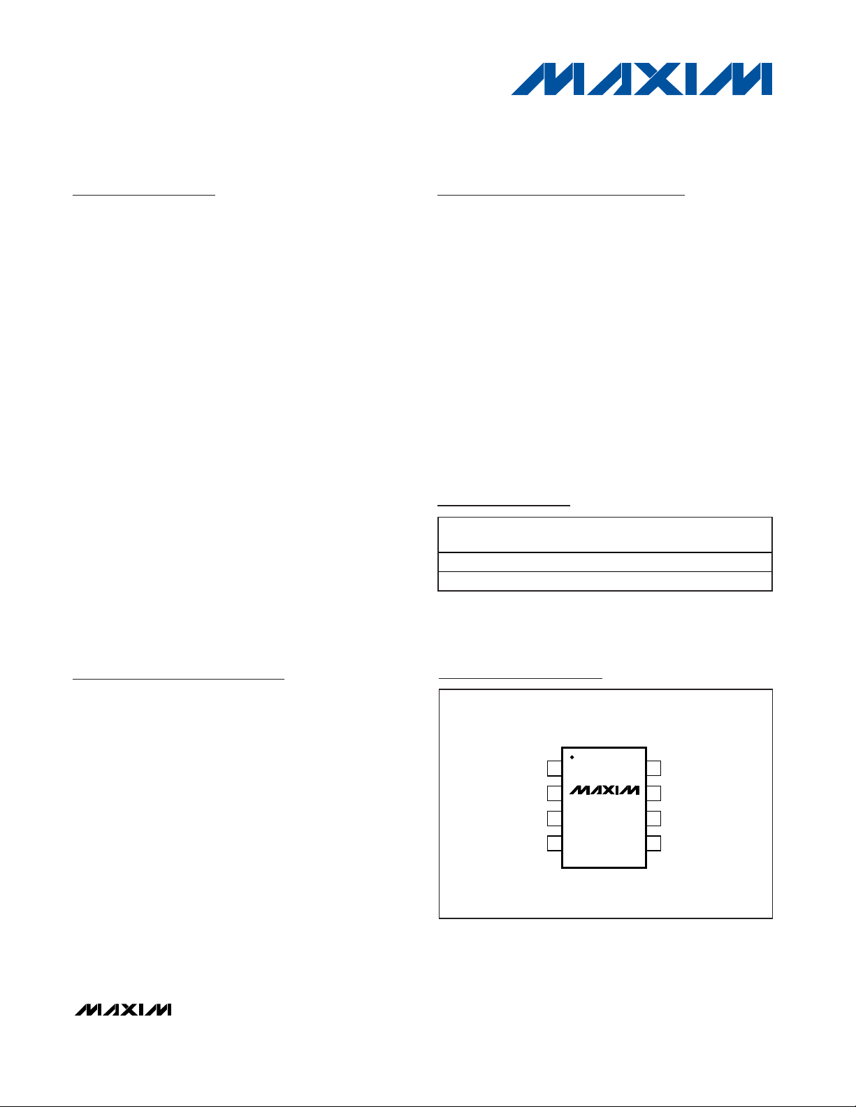
Pin Configuration
Ordering Information
19-3274; Rev 0; 5/04
For pricing, delivery, and ordering information, please contact Maxim/Dallas Direct! at
1-888-629-4642, or visit Maxim’s website at www.maxim-ic.com.
Typical Operating Circuit at end of data sheet.
PART
TEMP RANGE
PIN-
TOP
MARK
MAX3051ESA
8 SO —
MAX3051EKA-T
AEKF
PACKAGE
-40°C to +85°C
-40°C to +85°C 8 SOT23-8
MAX3051
+3.3V, 1Mbps, Low-Supply-Current
CAN Transceiver
2 _______________________________________________________________________________________
ABSOLUTE MAXIMUM RATINGS
ELECTRICAL CHARACTERISTICS
(VCC= +3.3V ±5%, RL= 60Ω, CL= 100pF, TA= T
MIN
to T
MAX
, unless otherwise noted. Typical values are at VCC= +3.3V and TA=
+25°C.) (Note 1)
Stresses beyond those listed under “Absolute Maximum Ratings” may cause permanent damage to the device. These are stress ratings only, and functional
operation of the device at these or any other conditions beyond those indicated in the operational sections of the specifications is not implied. Exposure to
absolute maximum rating conditions for extended periods may affect device reliability.
VCCto GND..............................................................-0.3V to +6V
TXD, RS, SHDN to GND...........................................-0.3V to +6V
RXD to GND .............................................................-0.3V to +6V
CANH, CANL to GND..........................................-7.5V to +12.5V
Continuous Power Dissipation (T
A
= +70°C)
8-Pin SO (derate 5.9mW/°C above +70°C)...................470mW
8-Pin SOT23 (derate 9.7mW/°C above +70°C).............774mW
Operating Temperature Range ...........................-40°C to +85°C
Maximum Junction Temperature .....................................+150°C
Storage Temperature Range.............................-65°C to +150°C
Lead Temperature Range (soldering, 10s)......................+300°C
PARAMETER
CONDITIONS
UNITS
Dominant 35 70
Recessive 2 5
mA
Supply Current I
S
Standby 8 15 µA
Shutdown Current I
SHDN
V
SHDN
= VCC, TXD = VCC or floating 1 µA
Thermal-Shutdown Threshold V
TSH
°C
Thermal-Shutdown Hysteresis 25 °C
TXD INPUT LEVELS
High-Level Input Voltage V
IH
2
V
CC
+
V
Low-Level Input Voltage V
IL
0.8 V
Input Capacitance C
IN
5pF
Pullup Resistor R
INTXD
50
kΩ
CANH, CANL TRANSMITTER
V
TXD
= VCC, no load 2 2.3 3 V
Recessive Bus Voltage
V
CANH
,
V
CANL
V
TXD
= VCC, no load, VRS = V
CC
(standby mode)
mV
Off-State Output Leakage
µA
Input Leakage Current V
CC
= 0V, V
CANH
= V
CANL
= 5V
µA
CANH Output Voltage V
CANH
V
TXD
= 0V
V
CANL Output Voltage V
CANL
V
TXD
= 0V
V
V
TXD
= 0V 1.5 3.0
V
TXD
= 0V, RL = 45Ω 1.2 3.0
V
V
TXD
= VCC, no load
Differential Output
(V
CANH
-
V
TXD
= V
CC, RL
= 60Ω
mV
SYMBOL
MIN TYP MAX
+160
V
CANL
-2V < V
)
CANH, VCANL
-100 +100
< +7V, SHDN = HIGH -250 +250
-250 +250
2.45
-500 +50
-120 +12
0.3V
100
1.25
MAX3051
+3.3V, 1Mbps, Low-Supply-Current
CAN Transceiver
_______________________________________________________________________________________ 3
ELECTRICAL CHARACTERISTICS (continued)
(VCC= +3.3V ±5%, RL= 60Ω, CL= 100pF, TA= T
MIN
to T
MAX
, unless otherwise noted. Typical values are at VCC= +3.3V and TA=
+25°C.) (Note 1)
PARAMETER
CONDITIONS
UNITS
-7V ≤ V
CANH
≤ 0V
CANH Short-Circuit Current
Minimum foldback current -35
mA
CANL Short-Circuit Current
VCC ≤ V
CANL
≤ 12V
mA
RXD OUTPUT LEVELS
RXD High Output-Voltage Level V
OH
I = -1mA
0.8 x
V
RXD Low Output-Voltage Level V
OL
I = 4mA 0.4 V
D C BU S R EC EI VER ( V
T XD
= V
C C
; C A N H a n d C A N L e x t e r n a l l y dr iv e n ; - 7 V ≤ V
C A N H
, V
C A N L
≤ + 1 2 V, un le s s ot h e r w i s e sp e c if i e d )
-7V ≤ VCM ≤ +12V 0.5
Differential Input Voltage
(Recessive)
V
DIFF
VRS = VCC (standby mode) 0.5
V
Dominant 0.9
Differential Input Voltage
(Dominant)
V
DIFF
VRS = VCC (standby mode) 1.1
V
Differential Input Hysteresis
20 mV
CANH and CANL Input
Resistance
R
I
20 50 kΩ
Differential Input Resistance R
DIFF
40
kΩ
MODE SELECTION (RS)
Input Voltage for High Speed V
SLP
0.3 x
V
Input Voltage for Standby V
STBY
0.75 x
V
Slope-Control Mode Voltage
RRS = 25kΩ to 200kΩ
0.4 x
0.6 x
V
High-Speed Mode Current I
HS
VRS = 0
µA
SHUTDOWN (SHDN)
SHDN Input Voltage High
2V
SHDN Input Voltage Low
0.8 V
SHDN Pulldown Resistor
50
kΩ
SYMBOL
I
CANHSC
I
CANLSC
V
D IF F( H Y S T )
V
SLOPE
V
SHDNH
V
SHDNL
R
INSHDN
MIN TYP MAX
-200
V
CC
V
V
CC
CC
200
V
CC
100
V
CC
V
CC
-500
100
MAX3051
+3.3V, 1Mbps, Low-Supply-Current
CAN Transceiver
4 _______________________________________________________________________________________
Note 1: All currents into device are positive; all currents out of the device are negative. All voltages are referenced to device
ground, unless otherwise noted.
Note 2: No other devices on the BUS.
Note 3: BUS externally driven.
TIMING CHARACTERISTICS
(VCC= +3.3V ±5%, RL= 60Ω, CL= 100pF, TA= T
MIN
to T
MAX
, unless otherwise noted. Typical values are at VCC= +3.3V and TA=
+25°C.)
PARAMETER
SYMBOL
CONDITIONS MIN TYP MAX
UNITS
VRS = 0V (≤1Mbps) 50
RRS = 25kΩ (≤500kbps) 183
Delay TXD to Bus Active
(Figure 1)
t
ONTXD
RRS = 100kΩ (≤125kbps) 770
ns
VRS = 0V (≤1Mbps) 70
RRS = 25kΩ (≤500kbps) 226
Delay TXD to Bus Inactive
(Figure 1)
RRS = 100kΩ (≤125kbps) 834
ns
VRS = 0V (≤1Mbps) 80
RRS = 25kΩ (≤500kbps) 200
Delay Bus to Receiver Active
(Figure 1)
RRS = 100kΩ (≤125kbps) 730
ns
VRS = 0V (≤1Mbps) 100
RRS = 25kΩ (≤500kbps) 245
Delay Bus to Receiver Inactive
(Figure 1)
RRS = 100kΩ (≤125kbps) 800
ns
VRS = 0V (≤1Mbps) 96
RRS = 25kΩ (≤500kbps) 12.5
RRS = 100kΩ (≤125kbps) 2.9
Differential-Output Slew Rate SR
R
RS
= 200kΩ (≤62.5kbps) 1.6
V/µs
Bus Dominant to RXD Active t
DRXDL
VRS > 0.8 x VCC, standby, Figure 2 1 µs
Standby to Receiver Active
BUS dominant, Figure 2 4 µs
SHDN to Bus Inactive
TXD = GND, Figure 3 (Note 2) 1 µs
S H DN to Recei ver Acti ve
BUS dominant, Fi gur e 3 (Note 3) 4 µs
S H D N to S tand b y
Fi g ur e 4 20 µs
t
OFFTXD
t
ONRXD
t
OFFRXD
t
SBRXDL
t
OFFSHDN
t
ONSHDN
t
SHDNSB
MAX3051
+3.3V, 1Mbps, Low-Supply-Current
CAN Transceiver
_______________________________________________________________________________________ 5
TXD
V
DIFF
0.9V
RXD
0.5V
VCC/2 VCC/2
t
ONTXD
t
ONRXD
t
OFFTXD
t
OFFRXD
VCC/2 VCC/2
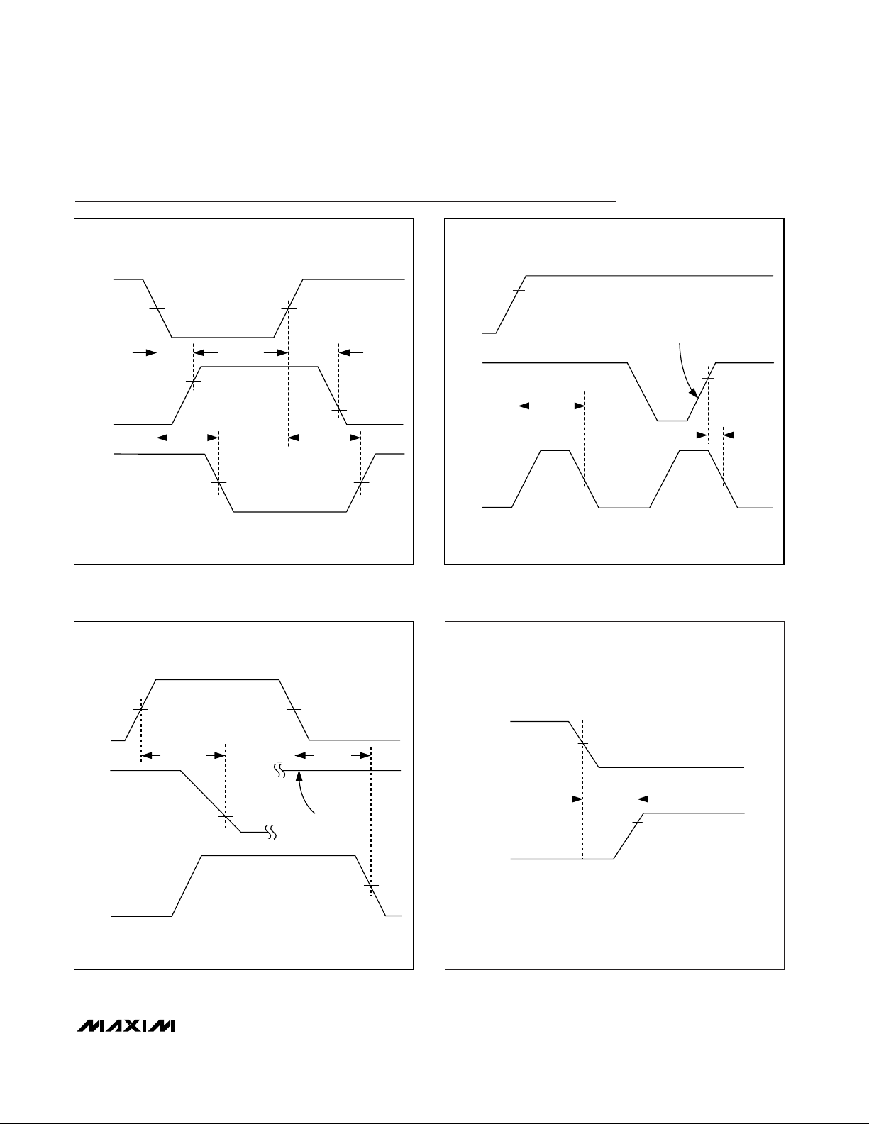
Figure 1. Timing Diagram Figure 2. Timing Diagram for Standby Signal
Figure 3. Timing Diagram for Shutdown Signal
0.75V × V
CC
RS
SHDN
VCC/2
t
SHDNSB
Figure 4. Timing Diagram for Shutdown-to-Standby Signal
Timing Diagrams
V
RS
DIFF
RXD
x 0.75
V
CC
t
SBRXDL
VCC/2 VCC/2
BUS EXTERNALLY
SHDN
VCC/2
V
/2
CC
DRIVEN
1.1V
t
DRXDL
t
OFFSHDN
V
DIFF
0.5V
RXD
t
ONSHDN
BUS EXTERNALLY
DRIVEN
/2
V
CC

SLEW RATE vs. RRS AT 100kbps
MAX3051toc01
RRS (kΩ)
SLEW RATE (V/µs)
18016014012010080604020
5
10
15
20
25
30
35
0
0200
MAX3051
+3.3V, 1Mbps, Low-Supply-Current
CAN Transceiver
6 _______________________________________________________________________________________
SUPPLY CURRENT vs. DATA RATE
MAX3051toc02
DATA RATE (kbps)
SUPPLY CURRENT (mA)
800600400200
13
16
19
22
25
10
0 1000
TA = +25°C
TA = -40°C
TA = +85°C
SHUTDOWN SUPPLY CURRENT vs.
TEMPERATURE (SHDN = V
CC
)
MAX3051toc03
TEMPERATURE (°C)
SHUTDOWN SUPPLY CURRENT (nA)
603510-15
20
40
60
80
100
120
0
-40 85
STANDBY SUPPLY CURRENT vs.
TEMPERATURE (RS = V
CC
)
MAX3051toc04
TEMPERATURE (°C)
STANDBY SUPPLY CURRENT (µA)
603510-15
8.5
9.0
9.5
10.0
10.5
11.0
8.0
-40 85
RECEIVER PROPAGATION DELAY vs.
TEMPERATURE
MAX3051toc05
TEMPERATURE (°C)
RECEIVER PROPAGATION DELAY (ns)
603510-15
5
10
15
20
25
30
35
40
45
50
0
-40 85
RRS = GND
RECESSIVE
DOMINANT
DRIVER PROPAGATION DELAY vs.
TEMPERATURE
MAX3051toc06
TEMPERATURE (°C)
DRIVER PROPAGATION DELAY (ns)
603510-15
10
20
30
40
50
0
-40 85
RRS = GND, DATA RATE = 100kbps
RECESSIVE
DOMINANT
RECEIVER OUTPUT LOW vs.
OUTPUT CURRENT
MAX3051toc07
OUTPUT CURRENT (mA)
VOLTAGE RXD (V)
40355 10 15 2520 30
0.2
0.4
0.6
0.8
1.0
1.2
1.4
1.6
0
045
TA = -85°C
TA = +25°C
TA = -40°C
Typical Operating Characteristics
(VCC= +3.3V, RL= 60Ω, CL= 100pF, TA= +25°C, unless otherwise specified.)

MAX3051
+3.3V, 1Mbps, Low-Supply-Current
CAN Transceiver
_______________________________________________________________________________________ 7
RECEIVER PROPAGATION DELAY
MAX3051toc10
RXD
1v/div
CAHN - CANL
200ns/div
RS = GND
DRIVER PROPAGATION DELAY
MAX3051toc11
TXD
2V/div
R
RS
= 24kΩ
R
RS
= 75kΩ
R
RS
= 100kΩ
200ns/div
DRIVER PROPAGATION DELAY
MAX3051toc12
TXD
1V/div
CAHN - CANL
200ns/div
RS = GND
LOOPBACK PROPAGATION DELAY
vs. R
RS
MAX3051toc13
RRS (kΩ)
LOOPBACK PROPAGATION DELAY (ns)
18016014012010080604020
200
400
600
800
1000
1200
0
0200
Typical Operating Characteristics (continued)
(VCC= +3.3V, RL= 60Ω, CL= 100pF, TA= +25°C, unless otherwise specified.)
RECEIVER OUTPUT HIGH vs.
OUTPUT CURRENT
MAX3051toc08
OUTPUT CURRENT (mA)
RECEIVER OUTPUT HIGH (V
CC
- RXD) (V)
71 2 3 54 6
0.2
0.4
0.6
0.8
1.0
1.2
1.4
1.6
1.8
0
08
DIFFERENTIAL VOLTAGE vs.
DIFFERENTIAL LOAD
MAX3051toc09
DIFFERENTIAL LOAD RL (Ω)
DIFFERENTIAL VOLTAGE (V)
200100
0.5
1.0
1.5
2.0
2.5
3.0
3.5
0
0300
TA = -85°C
TA = +25°C
TA = -40°C

MAX3051
+3.3V, 1Mbps, Low-Supply-Current
CAN Transceiver
8 _______________________________________________________________________________________
Detailed Description
PIN NAME FUNCTION
1 TXD
Transmit Data Input. TXD is a CMOS/TTL-compatible input from a CAN controller. TXD has an
internal 75kΩ pullup resistor.
2 GND Ground
3VCCSupply Voltage. Bypass VCC to GND with a 0.1µF capacitor.
4 RXD Receive Data Output. RXD is a CMOS/TTL-compatible output.
5 SHDN
Shutdown Input, CMOS/TTL-Compatible. Drive SHDN high to put the MAX3051 in shutdown.
SHDN has an internal 75kΩ pulldown resistor to GND.
6 CANL CAN Bus Line Low
7 CANH CAN Bus Line High
8RS
Mode-Select Input. Drive RS low or connect to GND for high-speed operation. Connect a resistor
between RS and GND to control output slope. Drive RS high to put into standby mode (see the
Mode Selection section).
Figure 5. MAX3051 Functional Diagram
V
CC
THERMAL
SHUTDOWN
V
CC
TXD
RS
RXD
MODE
SELECTION
TRANSMITTER
CONTROL
RECEIVER
MAX3051
SHUTDOWN
0.75V
CANH
CANL
GND
SHDN

MAX3051
+3.3V, 1Mbps, Low-Supply-Current
CAN Transceiver
_______________________________________________________________________________________ 9
Detailed Description
The MAX3051 interfaces between the CAN protocol
controller and the physical wires of the bus lines in a
CAN. It provides differential transmit capability to the
bus and differential receive capability to the CAN controller. It is primarily intended for +3.3V single-supply
applications that do not require the stringent fault protection specified by the automotive industry (ISO 11898)
The MAX3051 features four different modes of operation: high-speed, slope-control, standby, and shutdown
mode. High-speed mode allows data rates up to
1Mbps. The slope-control mode can be used to program the slew rate of the transmitter for data rates of up
to 500kbps. This reduces the effects of EMI, thus allowing the use of unshielded twisted or parallel cable. In
standby mode, the transmitter is shut off and the
receiver is pulled high, placing the MAX3051 in lowcurrent mode. In shutdown mode, the transmitter and
receiver are switched off.
The MAX3051 input common-mode range is from -7V to
+12V, exceeding the ISO 11898 specification of -2V to
+7V. These features, and the programmable slew-rate
limiting, make the part ideal for nonautomotive, harsh
environments.
The transceivers operate from a single +3.3V supply
and draw 35µA of supply current in dominant state and
2µA in recessive state. In standby mode, supply current is reduced to 8µA. In shutdown mode, supply current is less than 1µA.
CANH and CANL are output short-circuit current limited
and are protected against excessive power dissipation
by thermal-shutdown circuitry that places the driver
outputs into a high-impedance state.
Transmitter
The transmitter converts a single-ended input (TXD)
from the CAN controller to differential outputs for the
bus lines (CANH, CANL). The truth table for the transmitter and receiver is given in Table 1.
Receiver
The receiver reads differential inputs from the bus lines
(CANH, CANL) and transfers this data as a singleended output (RXD) to the CAN controller. It consists of
a comparator that senses the difference V
DIFF
= (CANH
- CANL) with respect to an internal threshold of +0.75V.
If this V
DIFF
is greater than 0.75, a logic-low is present at
RXD. If V
DIFF
is less than 0.75V, a logic-high is present.
The receiver always echoes the CAN BUS data.
The CANH and CANL common-mode range is -7V to
+12V. RXD is logic-high when CANH and CANL are
shorted or terminated and undriven.
Mode Selection
High-Speed Mode
Connect RS to ground to set the MAX3051 to highspeed mode. When operating in high-speed mode, the
MAX3051 can achieve transmission rates of up to
1Mbps. In high-speed mode, use shielded twisted pair
cable to avoid EMI problems.
Slope-Control Mode
Connect a resistor from RS to ground to select slopecontrol mode (Table 2). In slope-control mode, CANH
and CANL slew rates are controlled by the resistor connected to the RS pin. Maximum transmission speeds
are controlled by R
RS
and range from 40kbps to
500kbps. Controlling the rise and fall slopes reduces
EMI and allows the use of an unshielded twisted pair or
a parallel pair of wires as bus lines. The equation for
selecting the resistor value is given by:
R
RS
(kΩ) ≈ 12000 / (maximum speed in kbps)
See the Slew Rate vs. RRS graph in the Typical
Operating Characteristics.
Standby Mode
If a logic-high is applied to RS, the MAX3051 enters a
low-current standby mode. In this mode, the transmitter
TXD RS SHDN CANH CANL BUS STATE RXD
Low
V
RS
< 0.75 x
V
CC
Low High Low Dominant Low
High or float
V
RS
< 0.75 x
V
CC
Low
5kΩ to 25kΩ to
V
CC
/ 2
5kΩ to 25kΩ to
VCC / 2
Recessive High
X
V
RS
> 0.75 x
V
CC
Low
5kΩ to 25kΩ to
GND
5kΩ to 25kΩ to
GND
Recessive High
X X High Floating Floating Floating High
Table 1. Transmitter and Receiver Truth Table When Not Connected to The Bus

MAX3051
+3.3V, 1Mbps, Low-Supply-Current
CAN Transceiver
10 ______________________________________________________________________________________
is switched off and the receiver is switched to a lowcurrent/low-speed state. If dominant bits are detected,
RXD switches to low level. The microcontroller should
react to this condition by switching the transceiver back
to normal operation.
When the MAX3051 enters standby mode, RXD goes
high for 4µs (max) regardless of the BUS state.
However, after 4µs, RXD goes low only when the BUS
is dominant, otherwise RXD remains high (when the
BUS is recessive). For proper measurement of standbyto-receiver active time (t
SBRXDL
), the BUS should be in
dominant state (see Figure 2).
Shutdown
Drive SHDN high to enter shutdown mode. Connect
SHDN to ground or leave floating for normal operation.
Thermal Shutdown
If the junction temperature exceeds +160°C, the device
is switched off. The hysteresis is approximately 25°C,
disabling thermal shutdown once the temperature
drops below 135°C. In thermal shutdown, CANH and
CANL go recessive and all IC functions are disabled.
Applications Information
Reduced EMI and Reflections
In slope-control mode, the CANH and CANL outputs
are slew-rate limited, minimizing EMI and reducing
reflections caused by improperly terminated cables.
In multidrop CAN applications, it is important to maintain a direct point-to-point wiring scheme. A single pair
of wires should connect each element of the CAN bus,
and the two ends of the bus should be terminated with
120Ω resistors (Figure 6). A star configuration should
never be used.
Any deviation from the point-to-point wiring scheme
creates a stub. The high-speed edge of the CAN data
on a stub can create reflections back down the bus.
These reflections can cause data errors by eroding the
noise margin of the system.
Although stubs are unavoidable in a multidrop system,
care should be taken to keep these stubs as small as
possible, especially in high-speed mode. In slope-control mode, the requirements are not as rigorous, but
stub length should still be minimized.
Power Supply and Bypassing
The MAX3051 requires no special layout considerations
beyond common practices. Bypass VCCto GND with a
0.1µF ceramic capacitor mounted close to the IC with
short lead lengths and wide trace widths.
CONDITION FORCED AT PIN RS MODE RESULTING CURRENT AT RS
VRS < 0.3 x V
CC
High Speed |IRS| < 500µA
0.4 x VCC <VRS < 0.6 x V
CC
Slope Control 10µA < |IRS| < 200µA
VRS > 0.75 x V
CC
Standby |IRS| < 10µA
Table 2. Mode Selection Truth Table

MAX3051
+3.3V, 1Mbps, Low-Supply-Current
CAN Transceiver
______________________________________________________________________________________ 11
Chip Information
TRANSISTOR COUNT: 1024
PROCESS: BiCMOS
MAX3051
CAN
CONTROLLER
TXD
V
CC
RXD
RS
GND
CANH
CANL
V
CC
TX0
RX0
GND
0.1µF
120Ω
25kΩ TO 200kΩ
120Ω
Typical Operating Circuit
MAX3051
RL = 120Ω
R
L
= 120Ω
TRANSCEIVER 3
TRANSCEIVER 1
TXD
RXD
CANH
CANL
TWISTED PAIR
STUB
LENGTH
KEEP AS SHORT
AS POSSIBLE
TRANSCEIVER 2
Figure 6. Multiple Receivers Connected to CAN Bus

MAX3051
+3.3V, 1Mbps, Low-Supply-Current
CAN Transceiver
12 ______________________________________________________________________________________
Package Information
(The package drawing(s) in this data sheet may not reflect the most current specifications. For the latest package outline information
go to www.maxim-ic.com/packages
.)
SOICN .EPS
PACKAGE OUTLINE, .150" SOIC
1
1
21-0041
B
REV.DOCUMENT CONTROL NO.APPROVAL
PROPRIETARY INFORMATION
TITLE:
TOP VIEW
FRONT VIEW
MAX
0.010
0.069
0.019
0.157
0.010
INCHES
0.150
0.007
E
C
DIM
0.014
0.004
B
A1
MIN
0.053A
0.19
3.80 4.00
0.25
MILLIMETERS
0.10
0.35
1.35
MIN
0.49
0.25
MAX
1.75
0.050
0.016L
0.40 1.27
0.3940.386D
D
MINDIM
D
INCHES
MAX
9.80 10.00
MILLIMETERS
MIN
MAX
16
AC
0.337 0.344 AB8.758.55 14
0.189 0.197 AA5.004.80 8
N MS012
N
SIDE VIEW
H 0.2440.228 5.80 6.20
e 0.050 BSC 1.27 BSC
C
HE
e
B
A1
A
D
0∞-8∞
L
1
VARIATIONS:

MAX3051
+3.3V, 1Mbps, Low-Supply-Current
CAN Transceiver
Maxim cannot assume responsibility for use of any circuitry other than circuitry entirely embodied in a Maxim product. No circuit patent licenses are
implied. Maxim reserves the right to change the circuitry and specifications without notice at any time.
Maxim Integrated Products, 120 San Gabriel Drive, Sunnyvale, CA 94086 408-737-7600 ____________________ 13
© 2004 Maxim Integrated Products Printed USA is a registered trademark of Maxim Integrated Products.
Package Information (continued)
(The package drawing(s) in this data sheet may not reflect the most current specifications. For the latest package outline information
go to www.maxim-ic.com/packages
.)
SOT23, 8L .EPS
REV.DOCUMENT CONTROL NO.APPROVAL
PROPRIETARY INFORMATION
TITLE:
3.002.60E
C
E1
E
BETWEEN 0.08mm AND 0.15mm FROM LEAD TIP.
8. MEETS JEDEC MO178.
8∞
0.60
1.75
0.30
L2
0∞
e1
e
L
1.50E1
0.65 BSC.
1.95 REF.
0.25 BSC.
GAUGE PLANE
SEATING PLANE C
C
L
PIN 1
I.D. DOT
(SEE NOTE 6)
L
C
L
C
A2
e1
D
DETAIL "A"
5. COPLANARITY 4 MILS. MAX.
NOTE:
7. SOLDER THICKNESS MEASURED AT FLAT SECTION OF LEAD
6. PIN 1 I.D. DOT IS 0.3 MM ÿ MIN. LOCATED ABOVE PIN 1.
4. PACKAGE OUTLINE INCLUSIVE OF SOLDER PLATING.
3. PACKAGE OUTLINE EXCLUSIVE OF MOLD FLASH & METAL BURR.
HEEL OF THE LEAD PARALLEL TO SEATING PLANE C.
2. FOOT LENGTH MEASURED FROM LEAD TIP TO UPPER RADIUS OF
1. ALL DIMENSIONS ARE IN MILLIMETERS.
L2
L
A1
A
0.45
1.30
0.15
1.45
MAX
0.28b
0.90A2
0.00A1
0.90
A
MIN
SYMBOL
3.00
0.20
2.80D
0.09
C
SEE DETAIL "A"
L
C
b
e
D
1
21-0078
1
PACKAGE OUTLINE, SOT-23, 8L BODY
0
0

 Loading...