

19-0159; Rev 0; 9/93
Precision, Dual, High-Speed Analog Switches
__________________General Description
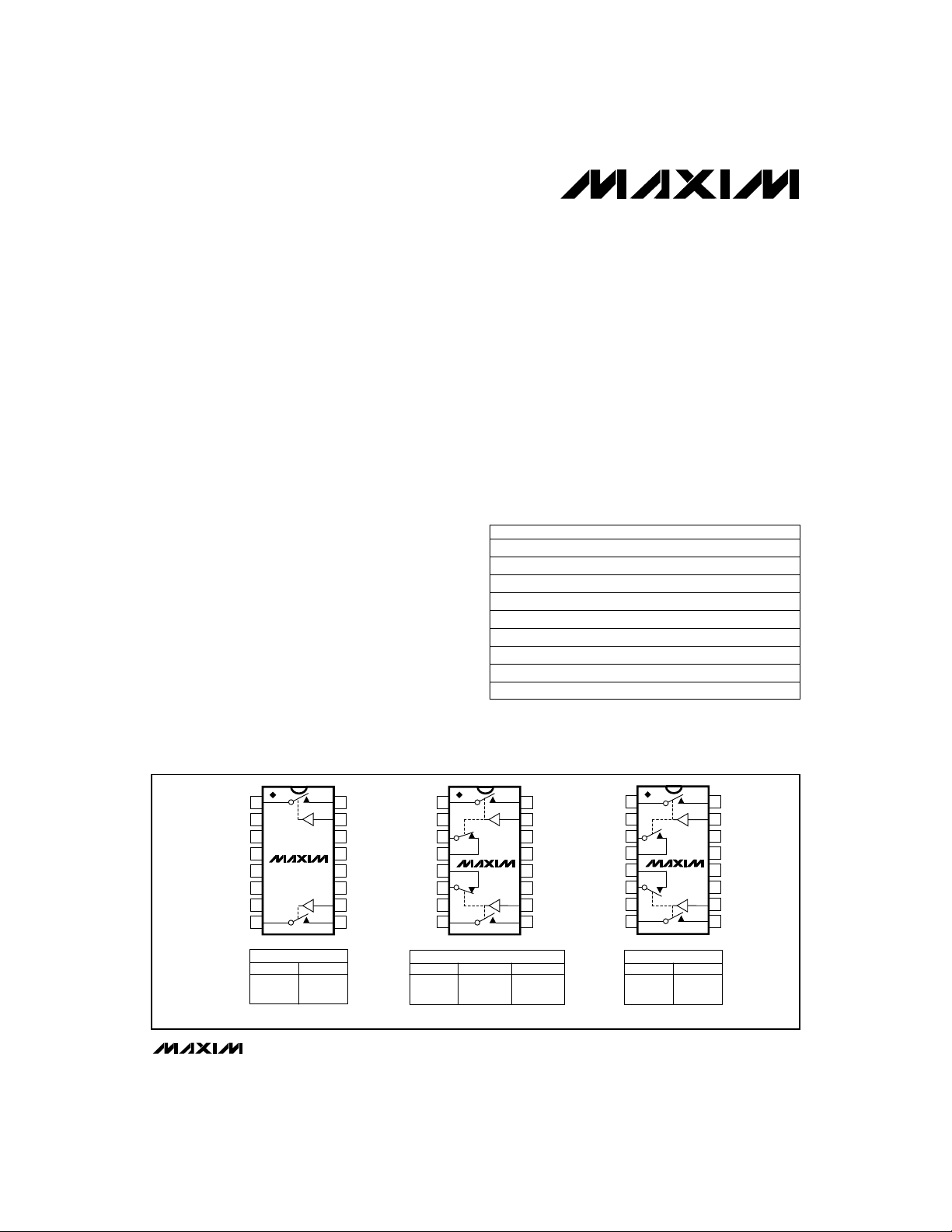
The MAX301/MAX303/MAX305 are precision, dual, highspeed analog switches. The single-pole single-throw (SPST)
MAX301 and double-pole single-throw (DPST) MAX305 dual
switches are normally open (NO). The single-pole doublethrow (SPDT) MAX303 has two NO and two normally closed
(NC) poles. All three parts offer low on resistance (less than
35Ω), guaranteed to match to within 2Ω between channels
and to remain flat over the full analog signal range (∆3Ω max).
They also offer low leakage (less than 250pA at +25°C and
less than 6nA at +85°C) and fast switching (turn-on time less
than 150ns and turn-off time less than 100ns).
The MAX301/MAX303/MAX305 are fabricated with Maxim’s
new improved silicon-gate process for high system accuracy.
Design improvements guarantee extremely low charge injection (15pC) and low power consumption (35µW). A 44V maximum breakdown voltage allows rail-to-rail analog signal
capability.
These monolithic switches operate with a single positive supply (+10V to +30V) or with split supplies (±4.5V to ±20V) while
retaining CMOS-logic input compatibility and fast switching.
CMOS inputs provide reduced input loading.
___________________________Applications
Sample-and-Hold Circuits Military Radios
Test Equipment Communication Systems
Heads-Up Displays Battery-Operated Systems
Guidance and Control Systems PBX, PABX
________________________________Features
♦ Low On Resistance <22Ω Typical (35Ω Max)
♦ Guaranteed Matched On Resistance Between
Channels <2Ω
♦ Guaranteed Flat On Resistance over Full Analog
Signal Range ∆3Ω Max
♦ Guaranteed Charge Injection <15pC
♦ Guaranteed Off-Channel Leakage <6nA at +85°C
♦ Single-Supply Operation (+10V to +30V)
Bipolar-Supply Operation (±4.5V to ±20V)
♦ TTL-/CMOS-Logic Compatible
♦ Rail-to-Rail Analog Signal Handling Capability
_________________Ordering Information
PART TEMP. RANGE PIN-PACKAGE
MAX301CPE 0°C to +70°C 16 Plastic DIP
MAX301CSE 0°C to +70°C 16 Narrow SO
MAX301CJE 0°C to +70°C 16 CERDIP
MAX301C/D 0°C to +70°C Dice*
MAX301EPE -40°C to +85°C 16 Plastic DIP
MAX301ESE -40°C to +85°C 16 Narrow SO
MAX301EJE -40°C to +85°C 16 CERDIP
MAX301MJE -55°C to +125°C 16 CERDIP
MAX301MLP -55°C to +125°C 20 LCC**
Ordering Information continued on last page.
* Contact factory for dice specifications.
** Contact factory for package availability.
___________________________Pin Configurations/Block Diagrams/Truth Tables
TOP VIEW
COM1
1
N.C.
2
N.C.
3
N.C.
4
N.C.
5
N.C.
N.C.
COM2
MAX301
6
7
8
DIP/SO
MAX301
LOGIC SWITCH
0
1
LCC packages on last page.
NO1
16
IN1
15
V-
14
GND
13
V
12
L
V+
11
IN2
10
NO2
9
OFF
ON
COM1
1
N.C.
2
COM3
3
NC3
4
NC4
5
COM4
N.C.
COM2
LOGIC SWITCHES 1, 2
0
1
SWITCHES SHOWN FOR LOGIC "0" INPUT
MAX303
6
7
8
DIP/SO
MAX303
OFF
ON
NO1
16
IN1
15
V-
14
GND
13
V
12
L
V+
11
IN2
10
NO2
9
SWITCHES 3, 4
ON
OFF
COM1
N.C.
COM3
NO3
NO4
COM4
N.C.
COM2
1
2
3
4
5
MAX305
6
7
8
DIP/SO
MAX305
LOGIC SWITCH
0
1
NO1
16
IN1
15
V-
14
GND
13
V
12
L
V+
11
IN2
10
NO2
9
OFF
ON
MAX301/MAX303/MAX305
_______________________________________________________________________
Maxim Integrated Products
Call toll free 1-800-998-8800 for free samples or literature.
1
Precision, Dual, High-Speed Analog Switches
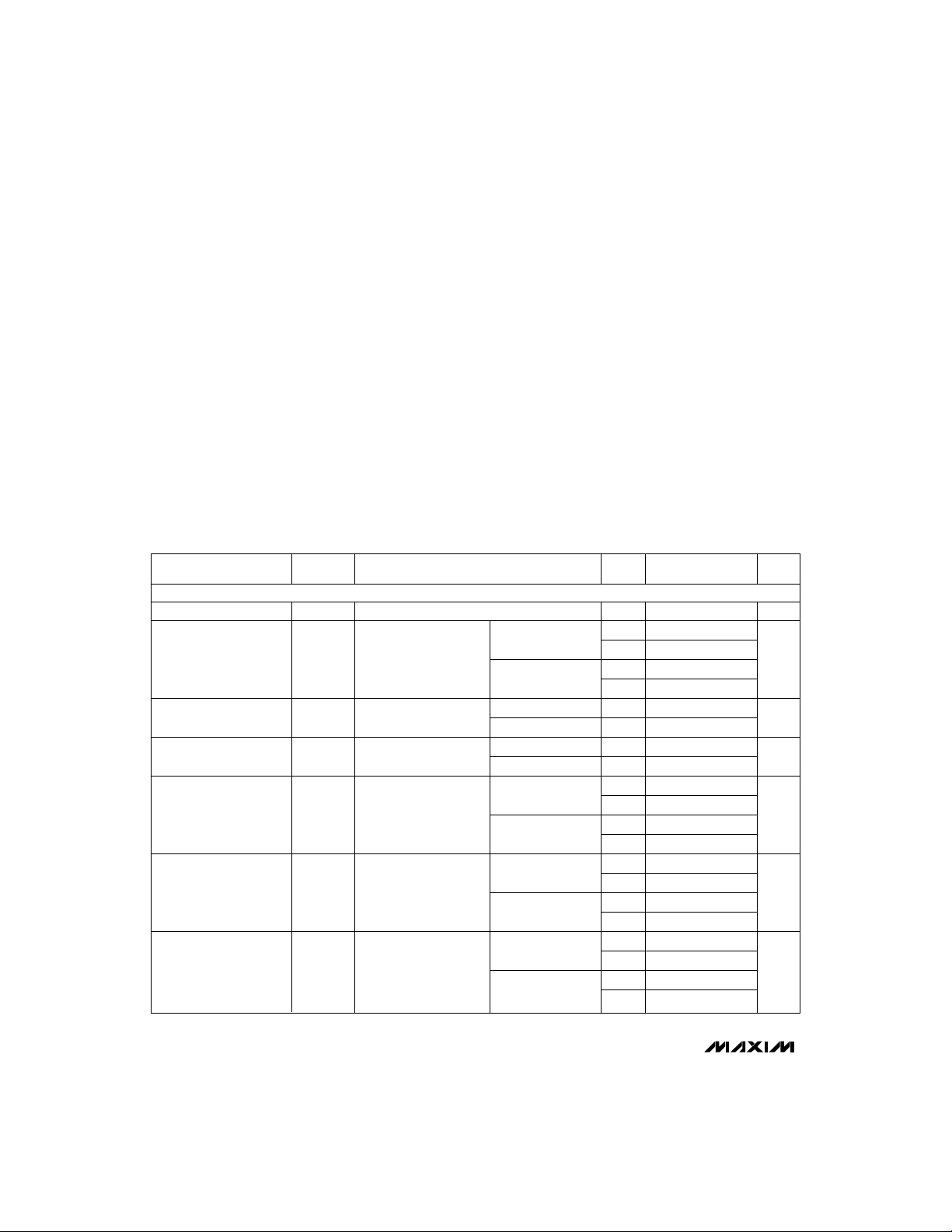
ABSOLUTE MAXIMUM RATINGS
Voltage Referenced to V-
V+.......................................................................................44V
GND ...................................................................................25V
.................................................................(GND-0.3V) to (V+) +0.3V
V
L
NO_, NC_, IN_, COM_ ................(V- - 2V) to (V+ + 2V) or 30mA,
..................................................................whichever occurs first
Continuous Current, COM_, NO_, NC_...............................30mA
Peak Current, COM_, NO_, NC_
(pulsed at 1ms, 10% duty cycle max) ..........................100mA
Continuous Power Dissipation (T
16-Pin Plastic DIP (derate 10.53mW/°C above +70°C) .....842mW
16-Pin Narrow SO (derate 8.70mW/°C above +70°C).......696mW
16-Pin CERDIP (derate 10.00mW/°C above +70°C)..........800mW
20-Pin LCC (derate 9.09mW/°C above +70°C)..................727mW
Operating Temperature Ranges:
MAX30_C_ _ .......................................................0°C to +70°C
MAX30_E_ _.....................................................-40°C to +85°C
MAX30_M_ _..................................................-55°C to +125°C
Storage Temperature Range.............................-65°C to +150°C
Lead Temperature (soldering, 10sec).............................+300°C
Note 1: Signals on NO_, NC_, or COM_ beyond V+ or V- are clamped by internal diodes. Limit forward current to maximum current rating.
Stresses beyond those listed under “Absolute Maximum Ratings” may cause permanent damage to the device. These are stress ratings only, and functional
operation of the device at these or any other conditions beyond those indicated in the operational sections of the specifications is not implied. Exposure to
absolute maximum rating conditions for extended periods may affect device reliability.
ELECTRICAL CHARACTERISTICS
(V+ = 15V, V- = -15V, VL= +5V, GND = 0V, V
PARAMETER SYMBOL CONDITIONS
SWITCH
Analog-Signal Range V
ANA
MAX301/MAX303/MAX305
On Resistance R
On Resistance Match
Between Channels (Note 4)
On Resistance Flatness
(Note 4)
NC or NO
Off Leakage Current
COM Off Leakage Current COM
COM On
Leakage Current
ON
R
ON
R
ON
NC_
(OFF)
or C, E -6 6
NO_
(OFF)
OFF
COM
ON
= +2.4V, V
INH
= +0.8V, TA= T
INL
MIN
to T
, unless otherwise noted.)
MAX
TEMP. MIN TYP MAX
RANGE (Note 2)
(Note 3) V- V+ V
C, E 20 35
M2030
C, E 55
MAX
M45
C, E, M 3
MAX
C, E, M 5
MAX
C, E -0.50 -0.01 0.50
M -0.25 -0.01 0.25
MAX
M -20 20
C, E -0.50 -0.01 0.50
M -0.25 -0.01 0.25
C, E -6 6
MAX
M -20 20
C, E -1.0 -0.04 1.0
M -0.4 -0.04 0.4
C, E -20 20
MAX
M -40.0 40.0
I
(NC or NO)
V
V
I
(NC or NO)
V
V+ = 15V, V- = -15V
IS= -10mA
V
V+ = 15V, V- = -15V
V
V
V+= 16.5V,V- =-16.5V
V
V
= ±10V
COM_
=2.4V,V
INH
= ±10V
COM_
= ±5V
COM_
= +15.5V,
COM_
NC_ or VNO_
= ±15.5V,
COM_
NC_ or VNO_
= -10mA,
=0.8V
INL
= -10mA,
= ±15.5V,
= +15.5V,
V+= 16.5V,V- =-16.5V
V
= ±15.5V,
COM_
V
NC_ or VNO_
V+= 16.5V,V- =-16.5V
= ±15.5V,
TA= +25°C
TA= T
T
TA= T
T
TA= T
to T
MIN
= +25°C C, E, M 0.5 2
A
to T
MIN
= +25°C C, E, M 3
A
to T
MIN
TA= +25°C
TA= T
MIN
to T
TA= +25°C
TA= T
MIN
to T
TA= +25°C
= T
T
to T
A
MIN
= +70°C) (Note 2)
A
UNITS
Ω
Ω
Ω
nA
nA
nA
2 ________________________________________________________________________________________________
Precision, Dual, High-Speed Analog Switches
ELECTRICAL CHARACTERISTICS (continued)
(V+ = 15V, V- = -15V, VL= +5V, GND = 0V, V
PARAMETER SYMBOL CONDITIONS
INPUT
Input Current with
Input Voltage High
Input Current with
Input Voltage Low
I
INH
I
INH
SUPPLY
Power-Supply Range ±4.5 ±20 V
Positive Supply Current
I+
Negative Supply Current I-
Logic Supply Current I
Ground Current I
L
GND
DYNAMIC
Turn-On Time t
Turn-Off Time t
Break-Before-Make
Time Delay (Note 3) Figure 2
ON
OFF
t
D
Charge Injection Q R
(Note 3) Figure 3
Off Isolation (Note 5) OIRR
Crosstalk (Note 6)
C
Off Capacitance
COM Off Capacitance
OFF
C
COM(OFF)
= +2.4V, V
INH
V
= 2.4V, all others = 0.8V
_
IN
V
= 0.8V, all others = 2.4V
_
IN
All channels on or off,
V
= 0V or 5V,
IN
V+ = 16.5V, V- = -16.5V
All channels on or off,
= 0V or 5V,
V
IN
V+ = 16.5V, V- = -16.5V
All channels on or off,
V
= 0V or 5V,
IN
V+ = 16.5V, V- = -16.5V
All channels on or off,
= 0V or 5V,
V
IN
V+ = 16.5V, V- = -16.5V
= +0.8V, TA= T
INL
to T
MIN
, unless otherwise noted.)
MAX
MIN TYP MAX
(Note 2)
-1.000 0.005 1.000 µA
-1.000 0.005 1.000 µA
= +25°C -1.00 0.01 1.00
T
A
= T
T
T
TA= T
to T
A
MIN
MAX
= +25°C -1.00 -0.01 1.00
A
to T
MIN
MAX
-5.00 5.00
-5.00 5.00
TA= +25°C -1.00 0.01 1.00
TA= T
MIN
to T
MAX
-5.00 5.00
TA= +25°C -1.00 -0.01 1.00
TA= T
MIN
to T
MAX
-5.00 5.00
UNITS
Figure1 TA= +25°C 100 150 ns
Figure 1 TA= +25°C 60 100 ns
MAX303 only,
= 10nF, V
C
L
= 0Ω,T
GEN
= 100Ω, CL= 5pF,
R
L
f = 1MHz, Figure 4
= 50Ω, CL= 5pF,
R
L
f = 1MHz, Figure 5
GEN
= 0V,
= +25°C 10 20 ns
T
A
= +25°C 10 15 pC
A
T
= +25°C 72 dB
A
T
= +25°C 90 dB
A
f = 1MHz, Figure 6 TA= +25°C 12 pF
f = 1MHz, Figure 6 TA= +25°C 12 pF
MAX301/MAX303/MAX305
µA
µA
µA
µA
Channel-On Capacitance C
COM(ON)
f = 1MHz, Figure 7 TA= +25°C 39 pF
Note 2: The algebraic convention, where the most negative value is a minimum and the most positive value a maximum, is used on
this data sheet.
Note 3: Guaranteed by design.
Note 4: ∆R
= ∆RONMAX - ∆RONMIN. On resistance match between channels and flatness are guaranteed only with
ON
specified voltages.
Note 5: See Figure 4. Off isolation = 20log10V
COM/VNC orVNO
, V
COM
= output, V
NC or VNO
= input to off switch.
Note 6: Between any two switches. See Figure 5.
_________________________________________________________________________________________________
3

Precision, Dual, High-Speed Analog Switches
________________________________________________T ypical Operating Characteristics
(TA = +25°C, unless otherwise noted).
ON RESISTANCE vs. V
POWER-SUPPLY VOLTAGE
A: V+ = 5V, V- = -5V
50
B: V+ = 10V, V- = -10V
C: V+ = 15V, V- = -15V
45
D: V+ = 20V, V- = -20V
40
35
(Ω)
30
ON
R
25
20
15
10
5
-20
-10 0 20
V
COM
ON RESISTANCE vs. V
70
MAX301/MAX303/MAX305
60
50
(Ω)
40
ON
R
30
20
V+ = 12V, V- = 0V
10
0
AND V- = OV
515
V
ANA
AND
COM
35
MAX301-1
D
MAX301-4
20
30
25
(Ω)
20
ON
R
15
10
100
10
.1
.01
OFF LEAKAGE (nA)
.001
.0001
A
B
C
10
(V)
COM
TA = +125°C
TA = +85°C
TA = +25°C
10
(V)
CHARGE INJECTION vs.
60
40
ANALOG VOLTAGE
ON RESISTANCE vs. V
AND TEMPERATURE
TA = +125°C
TA = +85°C
TA = +25°C
TA = -55°C
V+ = 15V, V- = -15V
5
1
-10 10
-20
OFF LEAKAGE CURRENTS vs.
TEMPERATURE
V+ = 16.5V
V- = -16.5V
V
= ±15V
COM
V
= ±15V
NC OR VNO
-55 125
TEMPERATURE (°C)
MAX301-7
COM
140
MAX301-2
120
100
(Ω)
80
ON
R
60
40
20
0
V
(V)
COM
25
20
MAX301-5
100
10
.01
ON LEAKAGE (nA)
.001
.0001
SUPPLY CURRENT vs.
100
10
ON RESISTANCE vs. V
WITH V- = 0V
V+ = 5V
V+ = 10V
V+ = 15V
0
515
10
V
(V)
COM
ON LEAKAGE CURRENTS vs.
TEMPERATURE
V+ = 16.5V
V- = -16.5V
= ±15V
V
COM
VNO = ±15V
V
NC OR
1
.1
-55 125
25
TEMPERATURE (°C)
TEMPERATURE
MAX301-8
COM
MAX301-3
V+ = 20V
20
MAX301-6
20
0
Q (pC)
-20
-40
V+ = 15V, V- = -15V
-60
-10 0
-20 20
V
(V)
COM
10
1
(µA)
L
.1
I+, I-, I
.01
.001
.0001
-55 125
I+ AT V+ = 16.5V
I- AT V- = -16.5V
IL AT VL = 5V
25
TEMPERATURE (°C)
4 _______________________________________________________________________________________

Precision, Dual, High-Speed Analog Switches
____________________Pin Descriptions
MAX301 PIN
DIP/SO
1, 8
2-7 N.C. Not internally connected
9, 16
10, 15 IN2, IN1 Digital Logic Inputs
11 V+
12 V
13 GND
14 V-
MAX303 PIN
DIP/SO
1, 8, 3, 6 2, 4, 8, 10 COM_ Drain (Analog Signal)
2-7
11 14 V+
12 15 V
13 17 GND Ground
14 18 V-
15, 10 19, 13 IN1, IN2 Digital Logic Inputs
16, 9, 5, 4
MAX305 PIN
DIP/SO
1, 8, 3, 6 2, 4, 8, 10 COM_ Drain (Analog Signal)
2-7
11 14 V+
12 15 V
13 17 GND Ground
14 18 V- Negative Supply Voltage
15, 10 19, 13 IN1, IN2 Digital Logic Inputs
16, 9, 5, 4
LCC
2, 10
1, 3-9, 11,
16
5, 7, 12,
20
13, 19
14
15
17
18
LCC
1, 3, 6, 9,
11, 16
5, 7, 12,20NC_,
LCC
1, 3, 6, 9,
11, 16
5, 7, 12,
20
NAME FUNCTION
COM1,
COM2
NC1,
NAME FUNCTION
NAME FUNCTION
Drain (Analog Signal)
Source (Analog Signal)
NC2
Positive Supply-Voltage
Input—connected to
substrate
Logic Supply-Voltage Input
L
Ground
Negative Supply Voltage
Input
N.C. Not internally connected
Positive Supply-Voltage
Input—connected to
substrate
Logic Supply-Voltage Input
L
Negative Supply Voltage
Input
Source (Analog Signal)
NO_
N.C. Not internally connected
Positive Supply-Voltage
Input—connected to
substrate
Logic Supply-Voltage Input
L
NO_ Source (Analog Signal)
__________Applications Information
Operation with Supply Voltages
The MAX301/MAX303/MAX305 switches operate with
±4.5V to ±20V bipolar supplies and a +10V to +30V single supply. In either case, analog signals ranging from V+
to V- can be switched. The
Characteristics
graphs show the typical on-resistance
variation with analog signal and supply voltage. The usual
on-resistance temperature coefficent is 0.5%/°C (typ).
The MAX301/MAX303/MAX305 operate with a single positive supply or with bipolar supplies. The devices maintain
TTL compatibility with supplies anywhere in the ±4.5V to
±20V range as long as VL= +5V. If VLis connected to V+
or another supply at voltages other than +5V, the devices
will operate at CMOS-logic level inputs.
Proper power-supply sequencing is recommended for all
CMOS devices. It is important not to exceed the absolute
maximum ratings because stresses beyond the listed ratings may cause permanent damage to the devices.
Always sequence V+ on first, followed by VL, V-, and
logic inputs. If power-supply sequencing is not possible,
add two small signal diodes in series with the supply pins
for overvoltage protection (Figure 1). Adding diodes
reduces the analog signal range to 1V below V+ and 1V
below V-, but low switch resistance and low leakage characteristics are unaffected. Device operation is
unchanged, and the difference between V+ to V- should
not exceed +44V.
NO_
V
g
Figure 1. Overvoltage Protection Using Blocking Diodes
Other than ±15V
Typical Operating
Logic Inputs
Overvoltage Protection
V+
COM_
V-
MAX301/MAX303/MAX305
________________________________________________________________________________________ 5

Precision, Dual, High-Speed Analog Switches
LOGIC
INPUT
SWITCH
INPUT
SWITCH
OUTPUT
SWITCH
INPUT
+3V
0V
V
COM
0V
-V
ANA
LOGIC INPUT WAVEFORM IS INVERTED FOR
SWITCHES THAT HAVE THE OPPOSITE LOGIC
SENSE CONTROL
50%
V
O
t
ON
V
O
0.9V
tr < 20ns
tf < 20ns
t
OFF
O
0.9V
= +10V
V
COM
for tON
= -10V
V
COM
for t
OFF
O
Figure 2. Switching-Time Test Circuit
V
+3V
LOGIC
INPUT
0V
V
COM
MAX301/MAX303/MAX305
SWITCH
OUTPUT
SWITCH
OUTPUT
0V
V
COM
0V
50%
V
O1
0.9V
O
V
O2
t
D
0.9V
O
t
D
V
COM_
COM_
LOGIC
INPUT
Figure 3. Break-Before-Make Test Circuit
+5V +15V
V+
SWITCH
INPUT
IN1
LOGIC
INPUT
FOR LOAD CONDITIONS, SEE
CL INCLUDES FIXTURE AND STRAY CAPACITANCE
= +10V
= +10V
IN_
CL INCLUDES FIXTURE AND STRAY CAPACITANCE.
LOGIC 0 INPUT.
L
COM
GND
0V
REPEAT TEST FOR EACH SWITCH
+5V
COM_
COM_
GND
V
L
0V
+15V
V+
NC_
V-
-15V
Electrical Characteristics.
NO
V+V
OR NO
V-
-15V
RL = 1000Ω
CL = 35pF
VO = V
V
O2
RL = 1000Ω
CL = 35pF
V
O
RL
COM
RL = R
C
L2
ON
V
O1
R
L1
C
L1
NC
V-
R
L2
+5V +15V
∆V
V
R
GEN
V
GEN
L
COM
GND
0V -15V
V+
NC OR NO
V-
C
10nF
V
O
L
V
O
INX
O
ON OFF ON
Q = (∆VO)(CL)
Figure 4. Charge-Injection Test Circuit
6 _______________________________________________________________________________________

Precision, Dual, High-Speed Analog Switches
+15V +5V
C
C
MAX301/MAX303/MAX305
SIGNAL
GENERATOR
ANALYZER
CH A
CH B
R
L
100Ω
Figure 5. Off Isolation
SIGNAL
GENERATOR
0V, 2.4V
ANALYZER
CH A
CH B
R
L
100Ω
Figure 6. Crosstalk Test Circuit
V+
V
COM
NC OR NO
GND
+15V +5V
C
V+
V+
COM
IN_
NC OR NO
GND
V
L
V-
-15V
V
L
V
NC OR NO
COM
V-
-15V
0V, 2.4V
IN_
C
C = 5pF
C
50Ω
IN2
0V, 2.4V
C
C = 5pF
FREQUENCY
TESTED
1 MHz
FREQUENCY
TESTED
1 MHz
SIGNAL
GENERATOR
AUTOMATIC
SYNTHESIZER
OFF ISOLATION = 20LOG
SIGNAL
GENERATOR
AUTOMATIC
SYNTHESIZER
V
COM
V
NC OR VNO
ANALYZER
TRACKING
SPECTRUM
ANALYZER
ANALYZER
TRACKING
SPECTRUM
ANALYZER
+15V
V+
COM
CAPACITANCE
METER
NC OR NO
GND
Figure 7. Channel-Off Capacitance
_______________________________________________________________________________________ 7
V+ V
-15V
+5V
CC
L
IN_
0V, 2.4V
C
V-
CAPACITANCE
METER
+15V +5V
V+
COM_
GND
-15V
CC
V
L
IN_
0V, 2.4V
C
V-
Figure 8. Channel-On Capacitance

Precision, Dual, High-Speed Analog Switches
__Ordering Information (continued)
PART TEMP.RANGE PIN-PACKAGE
MAX303CPE 0°C to +70°C 16 Plastic DIP
MAX303CSE 0°C to +70°C 16 Narrow SO
MAX303CJE 0°C to +70°C 16 CERDIP
MAX303C/D 0°C to +70°C Dice*
MAX303EPE -40°C to +85°C 16 Plastic DIP
MAX303ESE -40°C to +85°C 16 Narrow SO
MAX303EJE -40°C to +85°C 16 CERDIP
MAX303MJE -55°C to +125°C 16 CERDIP
MAX303MLP -55°C to +125°C 20 LCC**
MAX305CPE 0°C to +70°C 16 Plastic DIP
MAX305CSE 0°C to +70°C 16 Narrow SO
MAX305CJE 0°C to +70°C 16 CERDIP
MAX305C/D 0°C to +70°C Dice*
MAX305EPE -40°C to +85°C 16 Plastic DIP
MAX305ESE -40°C to +85°C 16 Narrow SO
MAX305EJE -40°C to +85°C 16 CERDIP
MAX305MJE -55°C to +125°C 16 CERDIP
MAX301/MAX303/MAX305
MAX305MLP -55°C to +125°C 20 LCC**
* Dice are tested at TA= +25°C only.
** Contact factory for availability.
_____Pin Configuration (continued)
TOP VIEW
COM3
COM4
N.C.
N.C.
N.C.
N.C.
N.C.
NC3
N.C.
NC4
5
6
7
8
5
6
7
8
N.C.
3
9
N.C.
N.C.
3
9
N.C.
MAX303
COM1
N.C.
2
1
MAX301
101112
N.C.
COM2
COM1
N.C.
2
1
101112
N.C.
COM2
NC1
20
NC2
NO1
20
NO2
IN1
19
184
V-
17
GND
16
N.C.
15
V
L
V+
14
13
IN2
IN1
19
V-
184
17
GND
N.C.
16
15
V
L
V+
14
13
IN2
COM1
N.C.
IN1
2
1
MAX305
101112
N.C.
COM2
NO1
20
NO2
19
184
V-
17
GND
16
N.C.
15
V
L
V+
14
13
IN2
N.C.
3
COM3
5
NO3
N.C.
6
7
NO4
8
COM4
9
N.C.
Maxim cannot assume responsibility for use of any circuitry other than circuitry entirely embodied in a Maxim product. No circuit patent licenses are
implied. Maxim reserves the right to change the circuitry and specifications without notice at any time.
8
______________________Maxim Integrated Products, 120 San Gabriel Drive, Sunnyvale, CA 94086 (408) 737-7600
© 1994 Maxim Integrated Products Printed USA is a registered trademark of Maxim Integrated Products.
 Loading...