

General Description
The MAX3000E/MAX3001E/MAX3002–MAX3012
8-channel level translators provide the level shifting necessary to allow data transfer in a multivoltage system.
Externally applied voltages, VCCand VL, set the logic levels on either side of the device. Logic signals present on
the VLside of the device appear as a higher voltage logic
signal on the VCCside of the device, and vice-versa.
The MAX3000E/MAX3001E/MAX3002/MAX3003 use an
architecture specifically designed to be bidirectional
without the use of a directional pin.
The MAX3000E/MAX3001E/MAX3002/MAX3004–MAX3012
feature an EN input that, when low, reduces the VCCand
VLsupply currents to < 2µA. The MAX3000E/MAX3001E
also have ±15kV ESD protection on the I/O V
CC
side for
greater protection in applications that route signals
externally. The MAX3000E operates at a guaranteed data
rate of 230kbps. The MAX3001E operates at a guaranteed
data rate of 4Mbps. The MAX3002–MAX3012 operate at a
guaranteed data rate of 20Mbps over the entire specified
operating voltage range.
The MAX3000E/MAX3001E/MAX3002–MAX3012 accept
VLvoltages from +1.2V to +5.5V and VCCvoltages from
+1.65V to +5.5V, making them ideal for data transfer
between low-voltage ASICs/PLDs and higher voltage
systems. The MAX3000E/MAX3001E/MAX3002–
MAX3012 are available in 20-bump UCSP™, 20-pin
TQFN (5mm x 5mm), and 20-pin TSSOP packages.
Applications
CMOS Logic-Level Translation
Cellphones
SPI™ and MICROWIRE™ Level Translation
Low-Voltage ASIC Level Translation
Smart Card Readers
Cellphone Cradles
Portable POS Systems
Portable Communication Devices
Low-Cost Serial Interfaces
GPS
Telecommunications Equipment
Features
♦ Guaranteed Data Rate Options
230kbps (MAX3000E)
4Mbps (MAX3001E)
20Mbps (MAX3002–MAX3012)
♦ Bidirectional Level Translation Without Using a
Directional Pin (MAX3000E/MAX3001E/MAX3002/
MAX3003)
♦ Unidirectional Level Translation
(MAX3004–MAX3012)
♦ Operation Down to +1.2V on V
L
♦ ±15kV ESD Protection on I/O VCCLines
(MAX3000E/MAX3001E)
♦ Ultra-Low 0.1µA Supply Current in Shutdown
♦ Low Quiescent Current (< 10µA)
♦ UCSP, TQFN, and TSSOP Packages
MAX3000E/MAX3001E/MAX3002–MAX3012
+1.2V to +5.5V, ±15kV ESD-Protected, 0.1µA,
35Mbps, 8-Channel Level Translators
________________________________________________________________ Maxim Integrated Products 1
Ordering Information
MAX3000E
MAX3001E
MAX3002–
MAX3012
+1.8V
+3.3V
+1.8V
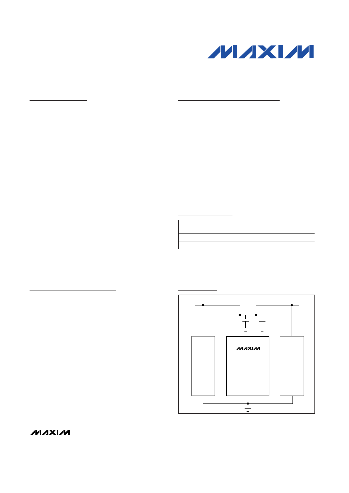
SYSTEM
CONTROLLER
+3.3V
SYSTEM
DATA DATA
GND
V
L
V
CC
I/O V
CC_
I/O V
L_
EN
Typical Operating Circuit
19-2672; Rev 4; 12/06
For pricing, delivery, and ordering information, please contact Maxim/Dallas Direct! at
1-888-629-4642, or visit Maxim’s website at www.maxim-ic.com.
PART
TEMP RANGE
PIN-
PACKAGE
PKG
CODE
MAX3000EEUP
-40°C to +85°C 20 TSSOP
U20-3
MAX3000EEBP-T
-40°C to +85°C 4 x 5 UCSP
B20-1
UCSP is a trademark of Maxim Integrated Products, Inc.
SPI is a trademark of Motorola, Inc.
MICROWIRE is a trademark of National Semiconductor.
Ordering Information continued at end of data sheet.
Pin Configurations and Functional Diagrams appear at end
of data sheet.
Note: All devices operate over the -40°C to +85°C operating
temperature range.
MAX3000E/MAX3001E/MAX3002–MAX3012
+1.2V to +5.5V, ±15kV ESD-Protected, 0.1µA,
35Mbps, 8-Channel Level Translators
2 _______________________________________________________________________________________
ABSOLUTE MAXIMUM RATINGS
Stresses beyond those listed under “Absolute Maximum Ratings” may cause permanent damage to the device. These are stress ratings only, and functional
operation of the device at these or any other conditions beyond those indicated in the operational sections of the specifications is not implied. Exposure to
absolute maximum rating conditions for extended periods may affect device reliability.
(All voltages referenced to GND.)
V
CC
...........................................................................-0.3V to +6V
V
L...........................................................................................
-0.3V to +6V
I/O V
CC_
......................................................-0.3V to (VCC+ 0.3V)
I/O V
L_
...........................................................-0.3V to (VL+ 0.3V)
EN, EN A/B ...............................................................-0.3V to +6V
Short-Circuit Duration I/O V
L_
, I/O V
CC_
to GND .......Continuous
Continuous Power Dissipation (T
A
= +70°C)
20-Pin TSSOP (derate 7.0mW/°C above +70°C) .........559mW
20-Bump UCSP (derate 10mW/°C above +70°C) .......800mW
20-Pin 5mm x 5mm TQFN
(derate 20.0mW/°C above +70°C)......................................1667mW
Operating Temperature Ranges
MAX3001EAUP..............................................-40°C to +125°C
MAX300_EE_P .................................................-40°C to +85°C
MAX30_ _E_P ..................................................-40°C to +85°C
Junction Temperature......................................................+150°C
Storage Temperature Range .............................-65°C to +150°C
Lead Temperature (soldering, 10s) .................................+300°C
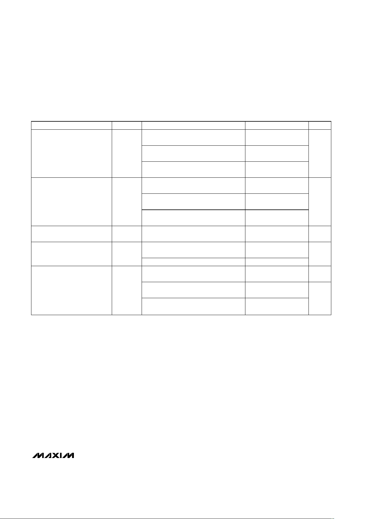
ELECTRICAL CHARACTERISTICS
(VCC= +1.65V to +5.5V, VL= +1.2V to VCC, EN = VL(MAX3000E/MAX3001E/MAX3002/MAX3004–MAX3012), EN A/B = VLor 0
(MAX3003), T
A
= T
MIN
to T
MAX
. Typical values are at VCC= +1.65V, VL= +1.2V, and TA= +25°C.) (Notes 1, 2)
PARAMETER
SYMBOL
CONDITIONS
MIN TYP MAX
UNITS
POWER SUPPLIES
VL Supply Range V
L
1.2
V
CC
V
VCC Supply Range V
CC
1.65 5.50
V
I/O V CC_ = 0, I/O V L _ = 0
or I/O V
CC
_ = VCC, I/O V L _ = VL,
MAX3000E/MAX3002–MAX3012
0.1 10
Supply Current from V
CC
I
QVCC
I/O V CC_ = 0, I/O V L _ = 0
or I/O V
CC
_ = VCC, I/O V L _ = VL,
MAX3001E
0.1 50
µA
I/O V CC_ = 0, I/O V L _ = 0
or I/O V
CC
_ = VCC, I/O V L _ = VL,
MAX3000E/MAX3002–MAX3012
0.1 10
Supply Current from V
L
I
QVL
I/O V CC_ = 0, I/O V L _ = 0
or I/O V
CC
_ = VCC, I/O V L _ = VL,
MAX3001E
0.1 50
µA
TA = +25°C, EN = 0,
MAX3000E/MAX3001E/MAX3002/
MAX3004–MAX3012
0.1 2
V
CC
Shutdown Supply Current
I
SHDN-VCC
TA = +25°C, EN A/B = 0,
MAX3003
0.1 2
µA
TA = +25°C, EN = 0,
MAX3000E/MAX3001E/MAX3002/
MAX3004–MAX3012
0.1 2
V
L
Shutdown Supply Current
I
SHDN-VL
TA = +25°C, EN A/B = 0,
MAX3003
0.1 2
µA
MAX3000E/MAX3001E/MAX3002–MAX3012
+1.2V to +5.5V, ±15kV ESD-Protected, 0.1µA,
35Mbps, 8-Channel Level Translators
_______________________________________________________________________________________ 3
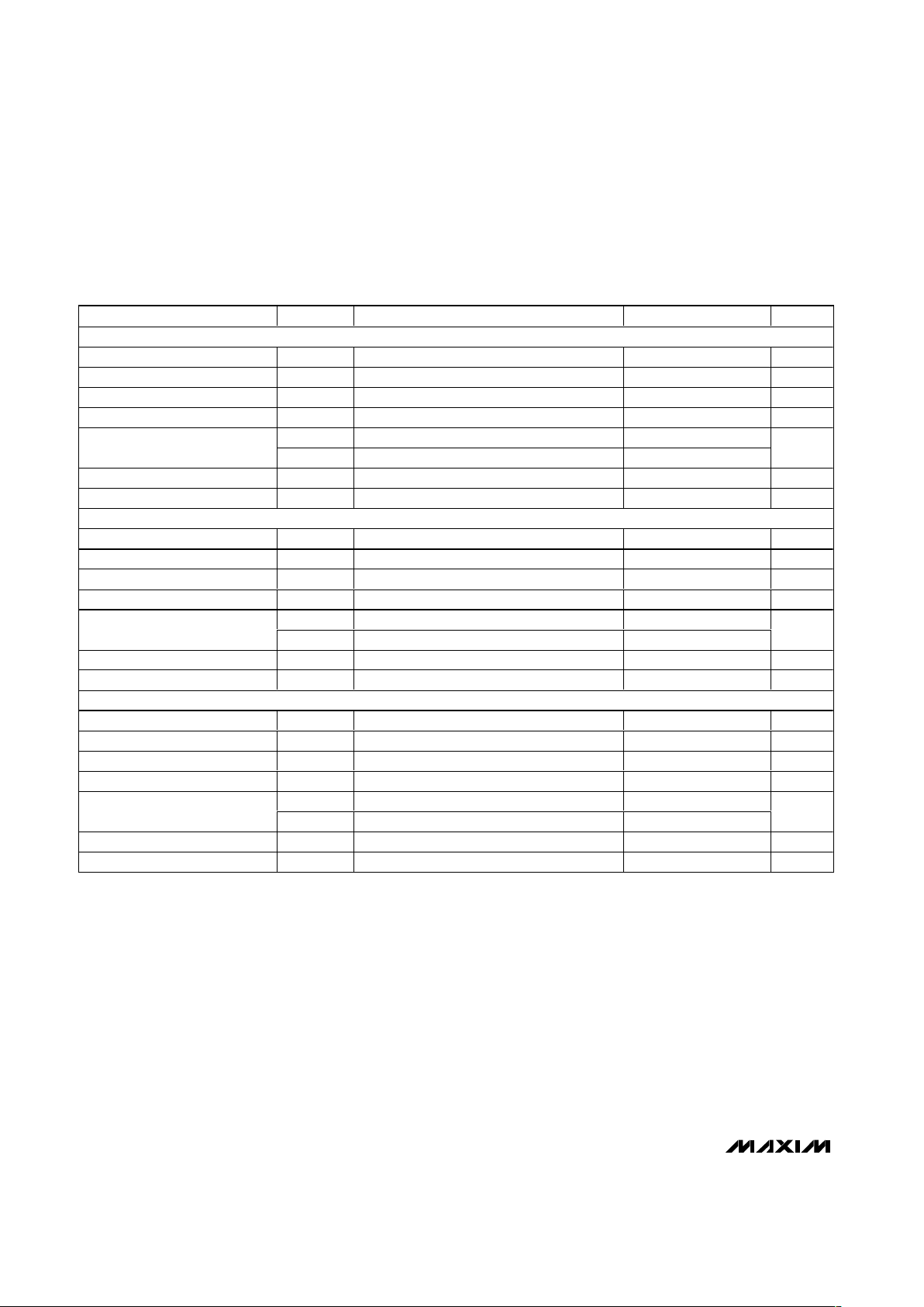
ELECTRICAL CHARACTERISTICS (continued)
(VCC= +1.65V to +5.5V, VL= +1.2V to VCC, EN = VL(MAX3000E/MAX3001E/MAX3002/MAX3004–MAX3012), EN A/B = VLor 0
(MAX3003), T
A
= T
MIN
to T
MAX
. Typical values are at VCC= +1.65V, VL= +1.2V, and TA= +25°C.) (Notes 1, 2)
PARAMETER
SYMBOL
CONDITIONS
MIN
TYP
MAX
UNITS
TA = +25°C, EN = 0,
MAX3000E/MAX3001E/MAX3002/
MAX3004–MAX3012
0.1 2
I/O V
CC
_ Three-State Output
Leakage Current
T
A
= +25°C, EN A/B = 0,
MAX3003
0.1 2
µA
I/O V
L
_ Three-State Output
Leakage Current
EN A/B = 0, MAX3003 0.1 2 µA
I/O V
L _
Pulldown Resistance
During Shutdown
EN = 0,
MAX3000E/MAX3001E/MAX3002/
MAX3004–MAX3012
4.59 8.30
kΩ
E N or EN A/B Inp ut Leakag e C ur rent
TA = +25°C1µA
LOGIC-LEVEL THRESHOLDS
I/O V
L
_ Input-Voltage High
Threshold
V
IHL
2/3 x V
L
V
I/O V
L
_ Input-Voltage Low
Threshold
V
ILL
1/3 x V
L
V
I/O V
CC
_ Input-Voltage High
Threshold
V
IHC
2/3 x V
CC
V
I/O V
CC
_ Input-Voltage Low
Threshold
V
ILC
1/3 x V
CC
V
EN, EN A/B Input-Voltage High
Threshold
V
IH
VL - 0.4
V
EN, EN A/B Input-Voltage Low
Threshold
V
IL
0.4 V
I/O VL _ Output-Voltage High V
OHL
I/O V
L
_ source current = 20µA, I/O V
CC
_ ≥
V
CC
- 0.4V
V
L
- 0.4 V
I/O V
L
_ Output-Voltage Low V
OLL
I/O VL _ sink current = 20µA,
I/O V
CC
_ ≤ 0.4V
0.4 V
I/O V
CC
_ Output-Voltage High V
OHC
I/O V
CC_
source current = 20µA, I/O V
L
_ ≥
V
L
- 0.4V
V
CC
- 0.4 V
I/O V
CC
_ Output-Voltage Low V
OLC
I/O V
CC
sink current = 20µA,
I/O V
L
_ ≤ 0.4V
0.4 V
ESD PROTECTION
I/O V
CC
_
Human Body Model,
MAX3000E/MAX3001E
±15
kV
MAX3000E/MAX3001E/MAX3002–MAX3012
+1.2V to +5.5V, ±15kV ESD-Protected, 0.1µA,
35Mbps, 8-Channel Level Translators
4 _______________________________________________________________________________________
TIMING CHARACTERISTICS
(VCC= +1.65V to +5.5V, VL= +1.2V to VCC, EN = VL(MAX3000E/MAX3001E/MAX3002/MAX3004–MAX3012), EN A/B = VLor 0
(MAX3003), T
A
= T
MIN
to T
MAX
. Typical values are at VCC= +1.65V, VL= +1.2V, and TA= +25°C.) (Notes 1, 2)
PARAMETER
SYM B O L
CONDITIONS
MIN TYP MAX
UNITS
RS = 50Ω , C
VCC
= 50p F, M AX 3000E ,
Fi g ur es 1a, 1b
400 800 1200
RS = 50Ω , C
VCC
= 50p F, M AX 3001E ,
Fi g ur es 1a, 1b
25 50
I/O VCC_ Rise Time t
RVCC
RS = 50Ω , C
VCC
= 50p F,
M AX 3002–M AX 3012, Fi g ur es 1a, 1b
15
ns
RS = 50Ω , C
VCC
= 50p F, M AX 3000E ,
Fi g ur es 1a, 1b
400 800 1200
RS = 50Ω , C
VCC
= 50p F, M AX 3001E ,
Fi g ur es 1a, 1b
25 50
I/O VCC_ Fall Time t
FVCC
RS = 50Ω , C
VCC
= 50p F,
M AX 3002–M AX 3012, Fi g ur es 1a, 1b
15
ns
RS = 50Ω , C VL = 50p F, M AX 3000E ,
Fi g ur es 2a, 2b
400 800 1200
RS = 50Ω , C VL = 50p F, M AX 3001E ,
Fi g ur es 2a, 2b
25 50
I/O V
L
_ Rise Time t
RVL
RS = 50Ω , C VL = 15p F,
M AX 3002–M AX 3012, Fi g ur es 2a, 2b
15
ns
RS = 50Ω , C VL = 50p F, M AX 3000E ,
Fi g ur es 2a, 2b
400 800 1200
RS = 50Ω , C VL = 50p F, M AX 3001E ,
Fi g ur es 2a, 2b
25 65
I/O V
L
_ Fall Time t
FVL
RS = 50Ω , C VL = 15p F,
M AX 3002–M AX 3012, Fi g ur es 2a, 2b
15
ns
RS = 50Ω , C
VCC
= 50p F, M AX 3000E ,
Fi g ur es 1a, 1b
1000
RS = 50Ω , C
VCC
= 50p F, M AX 3001E ,
Fi g ur es 1a, 1b
50
Propagation Delay
(Driving I/O V
L
_)
I/O
VL-VCC
RS = 50Ω , C
VCC
= 50p F,
M AX 3002–M AX 3012, Fi g ur es 1a, 1b
20
ns
RS = 50Ω , C VL = 50p F, M AX 3000E ,
Fi g ur es 2a, 2b
1000
RS = 50Ω , C VL = 50p F, M AX 3001E ,
Fi g ur es 2a, 2b
50
Propagation Delay
(Driving I/O V
CC
_)
I/O
VCC-VL
RS = 50Ω , C VL = 15p F,
M AX 3002–M AX 3012, Fi g ur es 2a, 2b
20
ns
Note 1: All units are 100% production tested at TA= +25°C. Limits over the operating temperature range are guaranteed by design
and not production tested.
Note 2: For normal operation, ensure that V
L
< VCC. During power-up, VL> VCCdoes not damage the device.
MAX3000E/MAX3001E/MAX3002–MAX3012
+1.2V to +5.5V, ±15kV ESD-Protected, 0.1µA,
35Mbps, 8-Channel Level Translators
_______________________________________________________________________________________ 5
TIMING CHARACTERISTICS (continued)
(VCC= +1.65V to +5.5V, VL= +1.2V to VCC, EN = VL(MAX3000E/MAX3001E/MAX3002/MAX3004–MAX3012), EN A/B = VLor 0
(MAX3003), T
A
= T
MIN
to T
MAX
. Typical values are at VCC= +1.65V, VL= +1.2V, and TA= +25°C.) (Notes 1, 2)
PARAMETER
SYM B O L
CONDITIONS
MIN
TYP
MAX
UNITS
RS = 50Ω , C
VCC
= 50p F, C VL = 50p F,
M AX 3000E
500
RS = 50Ω , C
VCC
= 50p F, C VL = 50p F,
M AX 3001E
10
Channel-to-Channel Skew t
SKEW
RS = 50Ω , C
VCC
= 50p F, C
VL
= 15p F,
M AX 3002–M AX 3012
5
ns
RS = 50Ω , C
V C C
= 50p F, C
V L
= 50p F,
∆T
A
= + 20°C , MAX3000E (N ote 3)
800
RS = 50Ω , C
VCC
= 50p F, C VL = 50p F,
∆T
A
= + 20°C , M AX 3001E ( N ote 3)
30
Part-to-Part Skew
t
PPSKEW
RS = 50Ω , C
VCC
= 50p F, C VL = 15p F,
∆T
A
= + 20°C , M AX 3002–M AX 3012 ( N ote 3)
10
ns
Propagation Delay from
I/O V
L _
to I/O V
CC_
after EN
t
EN-VCC
C
VCC
= 50p F, M AX 3000E /M AX 3001E ,
M AX 3002–M AX 3012, Fi g ur e 3
2µs
C VL = 50p F, M AX 3000E /M AX 3001E /
M AX 3002/M AX 3004–M AX 3012, Fi g ur e 4
2
Propagation Delay from
I/O V
CC_
to I/O V
L _
after EN
t
EN-VL
C VL = 15p F, M AX 3003, Fi g ur e 4 2
µs
RS = 50Ω , C
VCC
= 50p F, C VL = 50p F,
M AX 3000E
230
kbps
RS = 50Ω , C
VCC
= 50p F, C VL = 50p F,
M AX 3001E
4
Maximum Data Rate
R
S
= 50Ω , C
VCC
= 50p F, C VL = 15p F,
M AX 3002–M AX 3012
20
Mbps
Note 3: VCCfrom device 1 must equal VCCof device 2; VLfrom device 1 must equal VLof device 2.
MAX3000E/MAX3001E/MAX3002–MAX3012
+1.2V to +5.5V, ±15kV ESD-Protected, 0.1µA,
35Mbps, 8-Channel Level Translators
6 _______________________________________________________________________________________
TIMING CHARACTERISTICS—MAX3002–MAX3012
(VCC= +1.65V to +5.5V, VL= +1.2V to VCC, EN = VL(MAX3002/MAX3004–MAX3012), EN A/B = VLor 0 (MAX3003), TA= T
MIN
to
T
MAX.
) (Notes 1, 2)
PARAMETER
SYM B O L
CONDITIONS
MIN
TYP
MAX
UNITS
+1.2V ≤ VL ≤ VCC ≤ +3.3V
I/O VCC_ Rise Time t
RVCC
15 ns
I/O VCC_ Fall Time t
FVCC
15 ns
I/O VL _ Rise Time t
RVL
15 ns
I/O VL _ Fall Time t
FVL
15 ns
I/O
VL-VCC
Driving I/O VL _15
Propagation Delay
I/O
VCC-VL
Driving I/O VCC_15
ns
Channel-to-Channel Skew t
SKEW
Each translator equally loaded
5ns
Maximum Data Rate
20
Mbps
+2.5V ≤ VL ≤ VCC ≤ +3.3V
I/O VCC_ Rise Time t
RVCC
8.5
ns
I/O VCC_ Fall Time t
FVCC
8.5
ns
I/O VL _ Rise Time t
RVL
8.5
ns
I/O VL _ Fall Time t
FVL
8.5
ns
I/O
VL-VCC
Driving I/O VL _
8.5
Propagation Delay
I/O
VCC-VL
Driving I/O VCC_
8.5
ns
Channel-to-Channel Skew t
SKEW
Each translator equally loaded 10 ns
Maximum Data Rate 35
Mbps
+1.8V ≤ VL ≤ VCC ≤ +2.5V
I/O VCC_ Rise Time t
RVCC
10 ns
I/O VCC_ Fall Time t
FVCC
10 ns
I/O VL _ Rise Time t
RVL
10 ns
I/O VL _ Fall Time t
FVL
10 ns
I/O
VL-VCC
Driving I/O VL _15
Propagation Delay
I/O
VCC-VL
Driving I/O VCC_10
ns
Channel-to-Channel Skew t
SKEW
Each translator equally loaded 5 ns
Maximum Data Rate 30
Mbps
MAX3000E/MAX3001E/MAX3002–MAX3012
+1.2V to +5.5V, ±15kV ESD-Protected, 0.1µA,
35Mbps, 8-Channel Level Translators
_______________________________________________________________________________________ 7
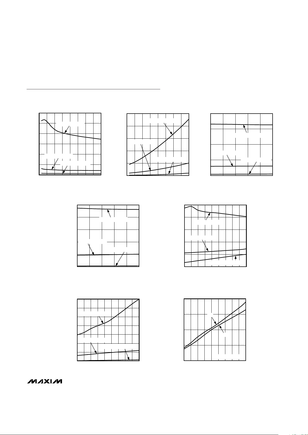
Typical Operating Characteristics
(TA = +25°C, unless otherwise noted.)
2000
1500
1000
500
0
-40 10-15 35 60 85
MAX3000E/01E/02-12 toc03
TEMPERATURE (°C)
V
L
SUPPLY CURRENT (µA)
VL SUPPLY CURRENT vs. TEMPERATURE
(DRIVING I/O V
CC
, VCC = 3.3V, VL = 1.8V)
DATA RATE = 20Mbps
DATA RATE = 4Mbps
DATA RATE = 230kbps
0
2000
6000
4000
8000
10,000
1.5 2.5 3.02.0 3.5 4.0 4.5 5.0 5.5
MAX3000E/01E/02-12 toc02
SUPPLY VOLTAGE (V)
V
CC
SUPPLY CURRENT (µA)
VCC SUPPLY CURRENT vs. SUPPLY VOLTAGE
(DRIVING I/O V
L
, VL = 1.8V)
DATA RATE = 230kbps
DATA RATE = 4Mbps
DATA RATE = 20Mbps
0
100
200
300
400
500
600
1.5 2.52.0 3.0 3.5 4.0 4.5 5.0 5.5
VL SUPPLY CURRENT vs. SUPPLY VOLTAGE
(DRIVING I/O V
L
, VL = 1.8V)
MAX3000E/01E/02-12 toc01
SUPPLY VOLTAGE (V)
V
L
SUPPLY CURRENT (µA)
DATA RATE = 20Mbps
DATA RATE = 4Mbps
DATA RATE = 230kbps
0
500
1500
1000
2000
2500
-40 10-15 35 60 85
MAX3000E/01E/02-12 toc04
TEMPERATURE (°C)
V
CC
SUPPLY CURRENT (µA)
VCC SUPPLY CURRENT vs. TEMPERATURE
(DRIVING I/O V
CC
, VCC = 3.3V, VL = 1.8V)
DATA RATE = 20Mbps
DATA RATE = 4Mbps
DATA RATE = 230kbps
0
20
40
60
80
100
10 40 5020 30 60 70 80 90 100
MAX3000E/01E/02-12 toc05
CAPACITIVE LOAD (pF)
V
L
SUPPLY CURRENT (µA)
VL SUPPLY CURRENT vs. CAPACITIVE LOAD ON
I/O V
CC
(DRIVING I/O VL, VCC = 3.3V, VL = 1.8V)
DATA RATE = 20Mbps
DATA RATE = 4Mbps
DATA RATE = 230kbps
0
2000
1000
4000
3000
6000
5000
7000
10 30 4020 50 60 70 80 90 100
MAX3000E/01E/02-12 toc06
CAPACITIVE LOAD (pF)
V
CC
SUPPLY CURRENT (µA)
VCC SUPPLY CURRENT vs. CAPACITIVE LOAD ON
I/O V
CC
(DRIVING I/O VL, VCC = 3.3V, VL = 1.8V)
DATA RATE = 20Mbps
DATA RATE = 4Mbps
DATA RATE = 230kbps
MAX3000E/01E/02-12 toc07
CAPACITIVE LOAD (pF)
RISE/FALL TIME (ns)
9080706050403020
500
1000
1500
2000
0
10 100
t
HL
MAX3000E
RISE/FALL TIME vs. CAPACITIVE LOAD ON
I/O V
CC
(DRIVING I/O VL, VCC = 3.3V, VL = 1.8V)
DATA RATE = 230kbps
t
LH
MAX3000E/MAX3001E/MAX3002–MAX3012
+1.2V to +5.5V, ±15kV ESD-Protected, 0.1µA,
35Mbps, 8-Channel Level Translators
8 _______________________________________________________________________________________
Typical Operating Characteristics (continued)
(TA = +25°C, unless otherwise noted.)
0
10
20
30
40
50
60
10 3020 40 50 60 70 80 90 100
MAX3000E/01E/02-12 toc08
CAPACITIVE LOAD (pF)
RISE/FALL TIME (ns)
MAX3001E
RISE/FALL TIME vs. CAPACITIVE LOAD ON
I/O V
CC
(DRIVING I/O VL, VCC = 3.3V, VL = 1.8V)
t
HL
t
LH
DATA RATE = 4Mbps
8
6
4
2
0
10 3020 40 50
MAX3000E/01E/02-12 toc09
CAPACITIVE LOAD (pF)
RISE/FALL TIME (ns)
MAX3002–MAX3012
RISE/FALL TIME vs. CAPACITIVE LOAD ON
I/O V
CC
(DRIVING I/O VL, VCC = 3.3V, VL = 1.8V)
t
LH
t
HL
DATA RATE = 20Mbps
0
500
1000
1500
2000
10 20
60
80
100
MAX3000E/01E/02-12 toc10
CAPACITIVE LOAD (pF)
RISE/FALL TIME (ns)
MAX3000E
RISE/FALL TIME vs. CAPACITIVE LOAD ON
I/O V
L
(DRIVING I/O VCC, VCC = 3.3V, VL = 1.8V)
30
40
50
70
90
t
LH
t
HL
DATA RATE = 230kbps
0
10
20
30
40
50
60
10 3020 40 50 60 70 80 90 100
MAX3000E/01E/02-12 toc11
CAPACITIVE LOAD (pF)
RISE/FALL TIME (ns)
MAX3001E
RISE/FALL TIME vs. CAPACITIVE LOAD ON
I/O V
L
(DRIVING I/O VCC, VCC = 3.3V, VL = 1.8V)
t
HL
t
LH
DATA RATE = 4Mbps
4
3
2
1
0
10 2015 25 30
MAX3000E/01E/02-12 toc12
CAPACITIVE LOAD (pF)
RISE/FALL TIME (ns)
MAX3002–MAX3012
RISE/FALL TIME vs. CAPACITIVE LOAD ON
I/O V
L
(DRIVING I/O VCC, VCC = 3.3V, VL = 1.8V)
t
LH
t
HL
DATA RATE = 20Mbps
0
100
200
300
400
500
10 40 5020 30 60 70 80 90 100
MAX3000E/01E/02-12 toc13
CAPACITIVE LOAD (pF)
PROPAGATION DELAY (ns)
DATA RATE = 230kbps
t
PHL
t
PLH
MAX3000E
PROPAGATION DELAY vs. CAPACITIVE LOAD ON
I/O V
CC
(DRIVING I/O VL, VCC = 3.3V, VL = 1.8V)

MAX3000E/MAX3001E/MAX3002–MAX3012
+1.2V to +5.5V, ±15kV ESD-Protected, 0.1µA,
35Mbps, 8-Channel Level Translators
_______________________________________________________________________________________ 9
Typical Operating Characteristics (continued)
(TA = +25°C, unless otherwise noted.)
0
100
200
300
400
500
600
10 3020 40 50 60 70 80 90 100
MAX3000E/01E/02-12 toc16
CAPACITIVE LOAD (pF)
PROPAGATION DELAY (ns)
MAX3000E
PROPAGATION DELAY vs. CAPACITIVE LOAD ON
I/O V
L
(DRIVING I/O VCC, VCC = 3.3V, VL = 1.8V)
t
PHL
t
PLH
DATA RATE = 230kbps
0
3
9
6
12
15
MAX3000E/01E/02-12 toc17
CAPACITIVE LOAD (pF)
PROPAGATION DELAY (ns)
10 3020 40 50
MAX3001E
PROPAGATION DELAY vs. CAPACITIVE LOAD ON
I/O V
L
(DRIVING I/O VCC, VCC = 3.3V, VL = 1.8V)
t
PLH
t
PHL
DATA RATE = 4Mbps
0
1
3
2
4
5
MAX3000E/01E/02-12 toc18
CAPACITIVE LOAD (pF)
PROPAGATION DELAY (ns)
10 2015 25 30
MAX3002–MAX3012
PROPAGATION DELAY vs. CAPACITIVE LOAD ON
I/O V
L
(DRIVING I/O VCC, VCC = 3.3V, VL = 1.8V)
t
PLH
t
PHL
DATA RATE = 20Mbps
1µs/div
MAX3000E RAIL-TO-RAIL DRIVING
(DRIVING I/O V
L
, VCC = 3.3V, VL = 1.8V,
CV
CC
= 50pF, DATA RATE = 230kbps)
GND
I/O V
L_
1V/div
GND
MAX3000E/01E/02-12 toc19
I/O V
CC_
2V/div
40ns/div
MAX3001E RAIL-TO-RAIL DRIVING
(DRIVING I/O V
L
, VCC = 3.3V, VL = 1.8V,
CV
CC
= 50pF, DATA RATE = 4Mbps)
GND
I/O V
L_
1V/div
GND
MAX3000E/01E/02-12 toc20
I/O V
CC_
2V/div
10ns/div
MAX3002–MAX3012 RAIL-TO-RAIL DRIVING
(DRIVING I/O V
L
, VCC = 3.3V, VL = 1.8V,
CV
CC
= 50pF, DATA RATE = 20Mbps)
GND
I/O V
L_
1V/div
GND
MAX3000E/01E/02-12 toc21
I/O V
CC_
2V/div
0
10
5
20
15
25
30
10 3020 40 50
MAX3000E/01E/02-12 toc14
CAPACITIVE LOAD (pF)
PROPAGATION DELAY (ns)
MAX3001E
PROPAGATION DELAY vs. CAPACITIVE LOAD ON
I/O V
CC
(DRIVING I/O VL, VCC = 3.3V, VL = 1.8V)
t
PHL
t
PLH
DATA RATE = 4Mbps
0
4
2
8
6
10
12
10 2015 25 30
MAX3000E/01E/02-12 toc15
CAPACITIVE LOAD (pF)
PROPAGATION DELAY (ns)
MAX3002–MAX3012
PROPAGATION DELAY vs. CAPACITIVE LOAD ON
I/O V
CC
(DRIVING I/O VL, VCC = 3.3V, VL = 1.8V)
t
PHL
t
PLH
DATA RATE = 20Mbps

MAX3000E/MAX3001E/MAX3002–MAX3012
+1.2V to +5.5V, ±15kV ESD-Protected, 0.1µA,
35Mbps, 8-Channel Level Translators
10 ______________________________________________________________________________________
Pin Description
PIN
TSSOP UCSP TQFN
NAME FUNCTION
1 B1 19 I/O VL1 Input/Output 1, Referenced to V
L
2A120 VLLogic Input Voltage, +1.2V ≤ VL ≤ VCC. Bypass VL to GND with a 0.1µF capacitor.
3 A2 1 I/O VL2 Input/Output 2, Referenced to V
L
4 B2 2 I/O VL3 Input/Output 3, Referenced to V
L
5 A3 3 I/O VL4 Input/Output 4, Referenced to V
L
6 B3 4 I/O VL5 Input/Output 5, Referenced to V
L
7 A4 5 I/O VL6 Input/Output 6, Referenced to V
L
8 B4 6 I/O VL7 Input/Output 7, Referenced to V
L
9 A5 7 I/O VL8 Input/Output 8, Referenced to V
L
10 B5 8 EN
Enable Input. If EN is pulled low, I/O V
CC
1 to I/O VCC8 are in three-state, while I/O VL1
to I/O V
L
8 have internal 6kΩ pulldown resistors. Drive EN high (VL) for normal
operation.
11 C5 9 GND Ground
12 D5 10
I/O VCC8
Input/Output 8, Referenced to V
CC
13 C4 11
I/O VCC7
Input/Output 7, Referenced to V
CC
14 D4 12
I/O VCC6
Input/Output 6, Referenced to V
CC
15 C3 13
I/O VCC5
Input/Output 5, Referenced to V
CC
16 D3 14
I/O VCC4
Input/Output 4, Referenced to V
CC
17 C2 15
I/O VCC3
Input/Output 3, Referenced to V
CC
18 D2 16
I/O VCC2
Input/Output 2, Referenced to V
CC
19 C1 17 V
CC
VCC Input Voltage, +1.65V ≤ VCC ≤ +5.5V. Bypass VCC to GND with a 0.1µF capacitor.
20 D1 18
I/O VCC1
Input/Output 1, Referenced to V
CC
——EP EP Exposed Pad. Connect to GND.
MAX3000E/MAX3001E/MAX3002

MAX3000E/MAX3001E/MAX3002–MAX3012
+1.2V to +5.5V, ±15kV ESD-Protected, 0.1µA,
35Mbps, 8-Channel Level Translators
______________________________________________________________________________________ 11
Pin Description (continued)
PIN
TSSOP UCSP TQFN
NAME FUNCTION
1B119
I/O VL1A
Input/Output 1A, Referenced to V
L
2A120 VLLogic Input Voltage, +1.2V ≤ VL ≤ VCC. Bypass VL to GND with a 0.1µF capacitor.
3A21
I/O VL2A
Input/Output 2A, Referenced to V
L
4B22
I/O VL3A
Input/Output 3A, Referenced to V
L
5A33
I/O VL4A
Input/Output 4A, Referenced to V
L
6B34
I/O VL1B
Input/Output 1B, Referenced to V
L
7A45
I/O VL2B
Input/Output 2B, Referenced to V
L
8B46
I/O VL3B
Input/Output 3B, Referenced to V
L
9A57
I/O VL4B
Input/Output 4B, Referenced to V
L
10 B5 8 EN A/B
Enable Input. If EN A/B is pulled low, channels 1B through 4B are active, and channels
1A through 4A are in three-state. If EN A/B is driven high to V
L
, channels 1A through 4A
are active, and channels 1B through 4B are in three-state.
11 C5 9 GND Ground
12 D5 10
I/O VCC4B
Input/Output 4B, Referenced to V
CC
13 C4 11
I/O VCC3B
Input/Output 3B, Referenced to V
CC
14 D4 12
I/O VCC2B
Input/Output 2B, Referenced to V
CC
15 C3 13
I/O VCC1B
Input/Output 1B, Referenced to V
CC
16 D3 14
I/O VCC4A
Input/Output 4A, Referenced to V
CC
17 C2 15
I/O VCC3A
Input/Output 3A, Referenced to V
CC
18 D2 16
I/O VCC2A
Input/Output 2A, Referenced to V
CC
19 C1 17 V
CC
VCC Input Voltage, +1.65V ≤ VCC ≤ +5.5V. Bypass VCC to GND with a 0.1µF capacitor.
20 D1 18
I/O VCC1A
Input/Output 1A, Referenced to V
CC
——EP EP Exposed Pad. Connect to GND.
MAX3003

MAX3000E/MAX3001E/MAX3002–MAX3012
+1.2V to +5.5V, ±15kV ESD-Protected, 0.1µA,
35Mbps, 8-Channel Level Translators
12 ______________________________________________________________________________________
Pin Description (continued)
NAME FUNCTION (Note 1)
V
CC
V
CC
Input Voltage, +1.65V < VCC < +5.5V. Bypass VCC to GND with a 0.1µF capacitor.
V
L
Logic Input Voltage, +1.2V ≤ VL ≤ VCC. Bypass VL to GND with a 0.1µF capacitor.
GND Ground
EN
(MAX3004)
Enable Input. If EN is pulled low, OVCC1–OVCC8 are in three-state, while IVL1–IVL8 have 6kΩ pulldown
resistors. Drive EN high (V
L
) for normal operation.
EN
(MAX3005)
Enable Input. If EN is pulled low, IVCC1 and OVCC2–OVCC8 are in three-state, while OVL1 and IVL2–IVL8 have
6kΩ pulldown resistors. Drive EN high (V
L
) for normal operation.
EN
(MAX3006)
Enable Input. If EN is pulled low, IVCC1, IVCC2, and OVCC3–OVCC8 are in three-state, while OVL1, OVL2, and
IV
L
3–IVL8 have 6kΩ pulldown resistors. Drive EN high (VL) for normal operation.
EN
(MAX3007)
Enable Input. If EN is pulled low, IVCC1, IVCC2, IVCC3, and OVCC4–OVCC8 are in three-state, while OVL1,
OV
L
2, OVL3, and IVL4–IVL8 have 6kΩ pulldown resistors. Drive EN high (VL) for normal operation.
EN
(MAX3008)
Enable Input. If EN is pulled low, IVCC1–IVCC4 and OVCC5–OVCC8 are in three-state, while OVL1–OVL4 and
IV
L
5–IVL8 have 6kΩ pulldown resistors. Drive EN high (VL) for normal operation.
EN
(MAX3009)
Enable Input. If EN is pulled low, IVCC1–IVCC5, OVCC6, OVCC7, and OVCC8 are in three-state, while
OV
L
1–OVL5, IVL6, IVL7, and IVL8 have 6kΩ pulldown resistors. Drive EN high (VL) for normal operation.
EN
(MAX3010)
Enable Input. If EN is pulled low, IVCC1–IVCC6, OVCC7, and OVCC8 are in three-state, while OVL1–OVL6, IVL7,
and IV
L
8 have 6kΩ pulldown resistors. Drive EN high (VL) for normal operation.
EN
(MAX3011)
Enable Input. If EN is pulled low, IVCC1–IVCC7 and OVCC8 are in three-state, while OVL1–OVL7 and IVL8 have
6kΩ pulldown resistors. Drive EN high (V
L
) for normal operation.
EN
(MAX3012)
Enable Input. If EN is pulled low, IVCC1–IVCC8 are in three-state, while OVL1–OVL8 have 6kΩ pulldown
resistors. Drive EN high (V
L
) for normal operation.
IVL1–IVL8 Inputs Referenced to VL, Numbers 1 to 8
OVL1–OVL8 Outputs Referenced to VL, Numbers 1 to 8
IVCC1–IVCC8 Inputs Referenced to VCC, Numbers 1 to 8
OVCC1–OVCC8
Outputs Referenced to VCC, Numbers 1 to 8
MAX3004–MAX3012
Note 1: For specific pin numbers, see the Pin Configurations.

MAX3000E/MAX3001E/MAX3002–MAX3012
+1.2V to +5.5V, ±15kV ESD-Protected, 0.1µA,
35Mbps, 8-Channel Level Translators
______________________________________________________________________________________ 13
______________________________________________Test Circuits/Timing Diagrams
MAX3000E/MAX3001E/
MAX3002/MAX3003
SOURCE
R
S
I/O V
L
EN
V
L
V
CC
I/O V
CC
C
VCC
I/O
VL-VCC
I/O
VL-VCC
I/O V
CC
I/O V
L
90%
50%
10%
90%
50%
10%
t
RISE/FALL
≤ 3ns
t
FVCC
t
RVCC
SOURCE
R
S
I/O V
L
EN
V
L
V
CC
I/O V
CC
C
VL
MAX3000E/MAX3001E/
MAX3002/MAX3003
I/O
VCC-VL
I/O
VCC-VL
I/O V
L
I/O V
CC
90%
50%
10%
90%
50%
10%
t
RISE/FALL
≤ 3ns
t
FVL
t
RVL
Figure 1a. Driving I/O V
L
Figure 1b. Timing for Driving I/O V
L
Figure 2a. Driving I/O V
CC
Figure 2b. Timing for Driving I/O V
CC

MAX3000E/MAX3001E/MAX3002–MAX3012
+1.2V to +5.5V, ±15kV ESD-Protected, 0.1µA,
35Mbps, 8-Channel Level Translators
14 ______________________________________________________________________________________
_________________________________Test Circuits/Timing Diagrams (continued)
SOURCE
EN
I/O V
CC
I/O V
L
C
VCC
V
L
EN
I/O V
L
I/O V
CC
t'
EN-VCC
V
L
V
L
V
CC
0
0
SOURCE
EN
I/O V
CC
I/O V
L
C
VCC
V
L
EN
I/O V
L
I/O V
CC
V
CC
2
t"
EN-VCC
V
L
V
L
V
CC
0
0
0
t
EN-VCC
IS WHICHEVER IS LARGER BETWEEN t'
EN-VCC
AND t"
EN-VCC
MAX3000E/MAX3001E/
MAX3002/MAX3003
MAX3000E/MAX3001E/
MAX3002/MAX3003
V
CC
2
Figure 3. Propagation Delay from I/O VLto I/O VCCAfter EN
SOURCE
EN
I/O V
CC
I/O V
L
C
VL
V
CC
EN
I/O V
L
I/O V
CC
t'
EN-VL
V
L
V
L
V
CC
0
0
0
SOURCE
EN
I/O V
CC
I/O V
L
C
VL
V
CC
EN
I/O V
L
I/O V
CC
t"
EN-VL
V
L
V
L
V
CC
0
0
0
t
EN-VL
IS WHICHEVER IS LARGER BETWEEN t'
EN-VL
AND t"
EN-VL
MAX3000E/MAX3001E/
MAX3002/MAX3003
MAX3000E/MAX3001E/
MAX3002/MAX3003
V
L
2
V
L
2
Figure 4. Propagation Delay from I/O VCCto I/O VLAfter EN

MAX3000E/MAX3001E/MAX3002–MAX3012
+1.2V to +5.5V, ±15kV ESD-Protected, 0.1µA,
35Mbps, 8-Channel Level Translators
______________________________________________________________________________________ 15
Detailed Description
The MAX3000E/MAX3001E/MAX3002–MAX3012 logiclevel translators provide the level shifting necessary to
allow data transfer in a multivoltage system. Externally
applied voltages, V
CC
and VL, set the logic levels on
either side of the device. Logic signals present on the
VLside of the device appear as a higher voltage logic
signal on the VCCside of the device, and vice-versa.
The MAX3000E/MAX3001E/MAX3002/MAX3003 are
bidirectional level translators allowing data translation
in either direction (VL↔ VCC) on any single data line.
These devices use an architecture specifically
designed to be bidirectional without the use of a direction pin. The MAX3004–MAX3012 unidirectional level
translators level shift data in one direction (VL → VCCor
V
CC
→ VL) on any single data line. The
MAX3000E/MAX3001E/ MAX3002–MAX3012 accept V
L
from +1.2V to +5.5V. All devices have VCCranging
from +1.65V to +5.5V, making them ideal for data transfer between low-voltage ASICs/PLDs and higher voltage systems.
The MAX3000E/MAX3001E/MAX3002/MAX3004–
MAX3012 feature an output enable mode that reduces
VCCsupply current to less than 2µA, and VLsupply
current to less than 2µA when in shutdown. The
MAX3000E/MAX3001E have ±15kV ESD protection on
the VCCside for greater protection in applications that
route signals externally. The MAX3000E operates at a
guaranteed data rate of 230kbps; the MAX3001E operates at a guaranteed data rate of 4Mbps and the
MAX3002–MAX3012 are guaranteed with a data rate of
20Mbps of operation over the entire specified operating
voltage range.
Level Translation
For proper operation, ensure that +1.65V ≤ VCC≤ +5.5V,
+1.2V ≤ VL≤ +5.5V, and VL≤ VCC. During power-up
sequencing, VL≥ VCCdoes not damage the device.
During power-supply sequencing, when VCCis floating
and VLis powering up, up to 10mA current can be
sourced to each load on the VL side, yet the device does
not latch up.
The maximum data rate also depends heavily on the
load capacitance (see the Typical Operating
Characteristics), output impedance of the driver, and
the operational voltage range (see the Timing
Characteristics table).
Input Driver Requirements
The MAX3001E/MAX3002–MAX3012 architecture is
based on a one-shot accelerator output stage. See
Figure 5. Accelerator output stages are always in three-
state except when there is a transition on any of the
translators on the input side, either I/O VLor I/O VCC.
When there is such a transition, the accelerator stages
become active, charging (discharging) the capacitances
at the I/Os. Due to its bidirectional nature, both stages
become active during the one-shot pulse. This can lead
to some current feeding into the external source that is
driving the translator. However, this behavior helps to
speed up the transition on the driven side.
For proper full-speed operation, the output current
of a device that drives the inputs of the MAX3000E/
MAX3001E/MAX3002–MAX3012 should meet the following requirements:
• MAX3000E (230kbps):
i > 1mA, R
drv
< 1kΩ
• MAX3001E (4Mbps):
i > 10
7
x V x (C + 10pF)
• MAX3002–MAX3012 (20Mbps):
i > 10
8
x V x (C + 10pF)
where i is the driver output current, V is the logic-supply
voltage (i.e., VLor VCC) and C is the parasitic capacitance of the signal line.
Enable Output Mode (EN, EN A/B)
The MAX3000E/MAX3001E/MAX3002 and the MAX3004–
MAX3012 feature an EN input, and the MAX3003 has an
EN A/B input. Pull EN low to set the MAX3000E/
MAX3001E/MAX3002/MAX3004–MAX3012s’ I/O VCC1
through I/O V
CC
8 in three-state output mode, while I/O
V
L
1 through I/O VL8 have internal 6kΩ pulldown resistors. Drive EN to logic-high (VL) for normal operation. The
MAX3003 is intended for bus multiplexing or bus switching applications. Drive EN A/B low to place channels 1B
through 4B in active mode, while channels 1A through
4A are in three-state mode. Drive EN A/B to logic-high
(V
L
) to enable channels 1A through 4A, while channels
1B through 4B remain in three-state mode.
±15kV ESD Protection
As with all Maxim devices, ESD-protection structures
are incorporated on all pins to protect against electrostatic discharges encountered during handling and
assembly. The I/O VCClines have extra protection
against static discharge. Maxim’s engineers have
developed state-of-the-art structures to protect these
pins against ESD of ±15kV without damage. The ESD
structures withstand high ESD in all states: normal
operation, three-state output mode, and powered
down. After an ESD event, Maxim’s E versions keep
working without latchup, whereas competing products
can latch and must be powered down to remove
latchup.

MAX3000E/MAX3001E/MAX3002–MAX3012
+1.2V to +5.5V, ±15kV ESD-Protected, 0.1µA,
35Mbps, 8-Channel Level Translators
16 ______________________________________________________________________________________
ESD protection can be tested in various ways. The
I/O V
CC
lines of the MAX3000E/MAX3001E are characterized for protection to ±15kV using the Human
Body Model.
ESD Test Conditions
ESD performance depends on a variety of conditions.
Contact Maxim for a reliability report that documents
test setup, test methodology, and test results.
Human Body Model
Figure 7a shows the Human Body Model and Figure 7b
shows the current waveform it generates when discharged into a low impedance. This model consists of
a 100pF capacitor charged to the ESD voltage of interest, which is then discharged into the test device
through a 1.5kΩ resistor.
Machine Model
The Machine Model for ESD tests all pins using a
200pF storage capacitor and zero discharge resistance. Its objective is to emulate the stress caused by
contact that occurs with handling and assembly during
manufacturing. Of course, all pins require this protection during manufacturing, not just inputs and outputs.
Therefore, after PCB assembly, the Machine Model is
less relevant to I/O ports.
P
ONE-SHOT
V
CC
V
L
I/O V
L
I/O V
CC
6kΩ
6kΩ
I/O V
CC_
TO I/O V
L_
PATH
I/O V
L_
TO I/O V
CC_
PATH
N
ONE-SHOT
P
ONE-SHOT
N
ONE-SHOT
Figure 5. MAX3001E/MAX3002–MAX3012 Simplified Functional Diagram (1 I/O Line)
0
V
TH_IN
/ 6kΩ
-(V
S
- V
TH_IN
) / 6kΩ
I
IN
V
TH_IN
V
S
V
IN
WHERE VS = VCC OR V
L
Figure 6. Typical IINvs. V
IN

Applications Information
Power-Supply Decoupling
To reduce ripple and the chance of transmitting incorrect data, bypass V
L
and VCCto ground with a 0.1µF
capacitor. To ensure full ±15kV ESD protection, bypass
VCCto ground with a 1µF capacitor. Place all capacitors as close to the power-supply inputs as possible.
I2C Level Translation
For I2C level translation for I2C applications, please refer
to the MAX3372E–MAX3379E/MAX3390E–MAX3393E
datasheet.
Unidirectional vs. Bidirectional Level
Translator
The MAX3000E/MAX3001E/MAX3002/MAX3003 bidirectional translators can operate as a unidirectional
device to translate signals without inversion. The
MAX3004–MAX3012 unidirecitional level translators,
level-shift data in one direction (VL→ VCCor VCC→ V
L)
on any single data line (see the Ordering Information.)
These devices provide the smallest solution (UCSP
package) for unidirectional level translation without
inversion.
MAX3000E/MAX3001E/MAX3002–MAX3012
+1.2V to +5.5V, ±15kV ESD-Protected, 0.1µA,
35Mbps, 8-Channel Level Translators
______________________________________________________________________________________ 17

MAX3000E/MAX3001E/MAX3002–MAX3012
+1.2V to +5.5V, ±15kV ESD-Protected, 0.1µA,
35Mbps, 8-Channel Level Translators
18 ______________________________________________________________________________________
HIGH-
VOLTAGE
DC
SOURCE
DEVICE
UNDER
TEST
R
C
1MΩ RD 1500Ω
CHARGE-CURRENT-
LIMIT RESISTOR
DISCHARGE
RESISTANCE
STORAGE
CAPACITOR
C
S
100pF
Figure 7a. Human Body ESD Test Model
100%
90%
36.8%
t
RL
t
DL
TIME
CURRENT WAVEFORM
PEAK-TO-PEAK RINGING
(NOT DRAWN TO SCALE)
10%
0
0
AMPERES
I
P
I
r
Figure 7b. Human Body Current Waveform
PART EN EN A/B Tx/Rx* DATA RATE
ESD PROTECTION
(kV)
MAX3000E √ — 8/8 230kbps ± 15
MAX3001E √ — 8/8 4Mbps ± 15
MAX3002 √ — 8/8 ** ± 2
MAX3003 — √ 8/8 ** ± 2
MAX3004 √ — 8/0 ** ± 2
MAX3005 √ — 7/1 ** ± 2
MAX3006 √ — 6/2 ** ± 2
MAX3007 √ — 5/3 ** ± 2
MAX3008 √ — 4/4 ** ± 2
MAX3009 √ — 3/5 ** ± 2
MAX3010 √ — 2/6 ** ± 2
MAX3011 √ — 1/7 ** ± 2
MAX3012 √ — 0/8 ** ± 2
Selector Guide
*T
x = V
L
→ V
CC
; R
x = V
CC
→ V
L
**See Table 1.
VL ↔ V
CC
(V)
MAX3002–MAX3012
GUARANTEED DATA RATE
(Mbps)
1.2 ↔ 5.5 40
1.2 ↔ 3.3 20
2.5 ↔ 3.3 35
1.8 ↔ 2.5 30
1.2 ↔ 2.5 20
1.2 ↔ 1.8 20
Table 1. Data Rate

MAX3000E/MAX3001E/MAX3002–MAX3012
+1.2V to +5.5V, ±15kV ESD-Protected, 0.1µA,
35Mbps, 8-Channel Level Translators
______________________________________________________________________________________ 19
MAX3000E/
MAX3001E/MAX3002
V
L
V
CC
EN
I/O V
L
1
I/O V
L
2
I/O V
L
3
I/O V
L
4
I/O VL5
I/O VL6
I/O V
L
7
I/O V
L
8 I/O VCC8
I/O V
CC
7
I/O V
CC
6
I/O V
CC
5
I/O VCC4
I/O VCC3
I/O V
CC
2
I/O V
CC
1
GND
MAX3000E/MAX3001E/MAX3002 Functional Diagram

MAX3000E/MAX3001E/MAX3002–MAX3012
+1.2V to +5.5V, ±15kV ESD-Protected, 0.1µA,
35Mbps, 8-Channel Level Translators
20 ______________________________________________________________________________________
MAX3003
V
L
V
CC
EN A/B
I/O V
L
1A
I/O V
L
2A
I/O V
L
3A
I/O V
L
4A
I/O VL1B
I/O VL2B
I/O V
L
3B
I/O V
L
4B I/O VCC4B
I/O V
CC
3B
I/O VCC2B
I/O VCC1B
I/O VCC4A
I/O VCC3A
I/O V
CC
2A
I/O V
CC
1A
GND
MAX3003 Functional Diagram

MAX3000E/MAX3001E/MAX3002–MAX3012
+1.2V to +5.5V, ±15kV ESD-Protected, 0.1µA,
35Mbps, 8-Channel Level Translators
______________________________________________________________________________________ 21
MAX3000E/MAX3001E/MAX3002
MAX3004–MAX3012
20 UCSP (Bottom View)
MAX3003
20 UCSP (Bottom View)
I/O VCC2V
CC
I/O VCC4 I/O VCC6
I/O VCC3I/O VCC1 I/O VCC5 I/O VCC7
I/O VL3I/O VL1 I/O VL5 I/O VL7
I/O VL2V
L
I/O VL4 I/O VL6
I/O VCC8
GND
EN
I/O VL8
1
B
A
C
D
2345
I/O VCC4AV
CC
I/O VCC2B I/O VCC4B
I/O VCC1BI/O VCC1A I/O VCC3B GND
I/O VL1BI/O VL1A I/O VL3B EN A/B
I/O VL4AV
L
I/O VL2B I/O VL4B
I/O VCC2A
I/O VCC3A
I/O VL3A
I/O VL2A
1
B
A
C
D
3452
20
19
18
17
16
15
14
13
1
2
3
4
5
6
7
8
V
L
I/O VL1
I/O V
L
2
I/O V
L
3
I/O V
L
4
I/O VL5
I/O V
L
6
I/O V
L
7
I/O V
L
8
EN
TOP VIEW
12
11
9
10
I/O VCC8
I/O V
CC
7
I/O V
CC
6
I/O V
CC
5
I/O V
CC
4
I/O V
CC
3
I/O VCC2
V
CC
I/O VCC1
GND
MAX3000E/MAX3001E/MAX3002
TSSOP
20
19
18
17
16
15
14
13
1
2
3
4
5
6
7
8
V
L
I/O VL1A
I/O V
L
2A
I/O V
L
3A
I/O V
L
4A
I/O VL1B
I/O V
L
2B
I/O V
L
3B
I/O V
L
4B
EN A/B
12
11
9
10
I/O VCC4B
I/O V
CC
3B
I/O V
CC
2B
I/O V
CC
1B
I/O V
CC
4A
I/O V
CC
3A
I/O VCC2A
V
CC
I/O VCC1A
GND
MAX3003
TSSOP
201918
17
V
L
I/O V
L
1A
I/O V
CC
1A
V
CC
16 I/O V
CC
2A
13
12
11
14
15
I/O V
CC
2B
*EXPOSED PADDLE
I/O V
CC
1B
I/O V
CC
4A
I/O V
CC
3A
I/O VCC3B
4
3
2
1
I/O VL1B
I/O V
L
4A
I/O V
L
3A
I/O V
L
2A
5I/O VL2B
6
7
8
9
I/O V
L
3B
I/O V
L
4B
EN A/B
I/O V
CC
4B
10
GND
TOP VIEW
5mm
✕
5mm THIN QFN
MAX3003
201918
17
V
L
I/O V
L
1
I/O V
CC
1
V
CC
16 I/O V
CC
2
13
12
11
14
15
I/O V
CC
6
*EXPOSED PADDLE
I/O V
CC
5
I/O V
CC
4
I/O V
CC
3
I/O VCC7
4
3
2
1
I/O VL5
I/O V
L
4
I/O V
L
3
I/O V
L
2
5I/O VL6
6
7
8
9
I/O V
L
7
I/O V
L
8
EN
GND
10I/O V
CC
8
5mm ✕ 5mm THIN QFN
MAX3000E/
MAX3001E/
MAX3002
Pin Configurations

MAX3000E/MAX3001E/MAX3002–MAX3012
+1.2V to +5.5V, ±15kV ESD-Protected, 0.1µA,
35Mbps, 8-Channel Level Translators
22 ______________________________________________________________________________________
20
19
18
17
16
15
14
13
1
2
3
4
5
6
7
8
V
L
I VL1
I V
L
2
I V
L
3
I V
L
4
I VL5
I V
L
6
I VL7
I V
L
8
EN
TOP VIEW
12
11
9
10
O VCC8
O V
CC
7
O V
CC
6
O V
CC
5
O VCC4
O V
CC
3
O V
CC
2
V
CC
O VCC1
GND
MAX3004
TSSOP
20
19
18
17
16
15
14
13
1
2
3
4
5
6
7
8
V
L
O VL1
I V
L
2
I V
L
3
I V
L
4
I VL5
I V
L
6
I VL7
I V
L
8
EN
12
11
9
10
O VCC8
O V
CC
7
O V
CC
6
O V
CC
5
O VCC4
O V
CC
3
O V
CC
2
V
CC
I VCC1
GND
MAX3005
TSSOP
20
19
18
17
16
15
14
13
1
2
3
4
5
6
7
8
V
L
O VL1
O V
L
2
I V
L
3
I V
L
4
I VL5
I V
L
6
I VL7
I V
L
8
EN
12
11
9
10
O VCC8
O V
CC
7
O V
CC
6
O V
CC
5
O VCC4
O V
CC
3
I V
CC
2
V
CC
I VCC1
GND
MAX3006
TSSOP
20
19
18
17
16
15
14
13
1
2
3
4
5
6
7
8
V
L
O VL1
O V
L
2
O V
L
3
I V
L
4
I V
L
5
I V
L
6
I VL7
I V
L
8
EN
12
11
9
10
O VCC8
O V
CC
7
O V
CC
6
O V
CC
5
O V
CC
4
I V
CC
3
I VCC2
V
CC
I VCC1
GND
MAX3007
TSSOP
20
19
18
17
16
15
14
13
1
2
3
4
5
6
7
8
V
L
O VL1
O V
L
2
O V
L
3
O V
L
4
I V
L
5
I V
L
6
I VL7
I V
L
8
EN
12
11
9
10
O VCC8
O V
CC
7
O V
CC
6
O V
CC
5
I V
CC
4
I V
CC
3
I VCC2
V
CC
I VCC1
GND
MAX3008
TSSOP
20
19
18
17
16
15
14
13
1
2
3
4
5
6
7
8
V
L
O VL1
O V
L
2
O V
L
3
O V
L
4
O V
L
5
I V
L
6
I VL7
I V
L
8
EN
12
11
9
10
O VCC8
O V
CC
7
O V
CC
6
I V
CC
5
I V
CC
4
I V
CC
3
I VCC2
V
CC
I VCC1
GND
MAX3009
TSSOP
Pin Configurations (continued)

MAX3000E/MAX3001E/MAX3002–MAX3012
+1.2V to +5.5V, ±15kV ESD-Protected, 0.1µA,
35Mbps, 8-Channel Level Translators
______________________________________________________________________________________ 23
20
19
18
17
16
15
14
13
1
2
3
4
5
6
7
8
V
L
O VL1
O V
L
2
O VL3
O V
L
4
O VL5
O V
L
6
I VL7
I V
L
8
EN
12
11
9
10
O VCC8
O V
CC
7
I V
CC
6
I V
CC
5
I VCC4
I V
CC
3
I VCC2
V
CC
I VCC1
GND
MAX3010
TSSOP
20
19
18
17
16
15
14
13
1
2
3
4
5
6
7
8
V
L
O VL1
O V
L
2
O VL3
O V
L
4
O VL5
O V
L
6
O VL7
I V
L
8
EN
12
11
9
10
O VCC8
I V
CC
7
I V
CC
6
I V
CC
5
I VCC4
I V
CC
3
I VCC2
V
CC
I VCC1
GND
MAX3011
TSSOP
20
19
18
17
16
15
14
13
1
2
3
4
5
6
7
8
V
L
O VL1
O V
L
2
O VL3
O V
L
4
O VL5
O V
L
6
O VL7
O V
L
8
EN
12
11
9
10
I VCC8
I V
CC
7
I V
CC
6
I V
CC
5
I VCC4
I V
CC
3
I VCC2
V
CC
I VCC1
GND
MAX3012
TSSOP
TOP VIEW
Pin Configurations (continued)
Ordering Information (continued)
*Future product—contact factory for availability.
-T = Tape-and-reel package.
PART
TEMP RANGE
PIN-
PACKAGE
PKG
CODE
MAX3001EEUP -40°C to +85°C
20 TSSOP
U20-3
MAX3001EEBP-T*
-40°C to +85°C
4 x 5 UCSP
B20-1
MAX3001EETP -40°C to +85°C 20 TQFN
T2055-4
MAX3001EAUP
-40°C to +125°C 20 TSSOP
U20-3
MAX3002EUP -40°C to +85°C
20 TSSOP
U20-3
MAX3002EBP-T*
-40°C to +85°C
4 x 5 UCSP
B20-1
MAX3002ETP -40°C to +85°C 20 TQFN
T2055-4
MAX3003EUP -40°C to +85°C
20 TSSOP
U20-3
MAX3003EBP-T*
-40°C to +85°C
4 x 5 UCSP
B20-1
MAX3003ETP -40°C to +85°C 20 TQFN
T2055-4
MAX3004EUP -40°C to +85°C
20 TSSOP
U20-3
MAX3004EBP-T*
-40°C to +85°C
4 x 5 UCSP
B20-1
MAX3005EUP -40°C to +85°C
20 TSSOP
U20-3
MAX3005EBP-T*
-40°C to +85°C
4 x 5 UCSP
B20-1
MAX3006EUP -40°C to +85°C
20 TSSOP
U20-3
MAX3006EBP-T*
-40°C to +85°C
4 x 5 UCSP
B20-1
PART TEMP RANGE
PINPACKAGE
PKG
CODE
MAX3007EUP -40°C to +85°C 20 TSSOP U20-3
MAX3007EBP-T* -40°C to +85°C 4 x 5 UCSP B20-1
MAX3008EUP -40°C to +85°C 20 TSSOP U20-3
MAX3008EBP-T* -40°C to +85°C 4 x 5 UCSP B20-1
MAX3009EUP -40°C to +85°C 20 TSSOP U20-3
MAX3009EBP-T* -40°C to +85°C 4 x 5 UCSP B20-1
MAX3010EUP -40°C to +85°C 20 TSSOP U20-3
MAX3010EBP-T* -40°C to +85°C 4 x 5 UCSP B20-1
MAX3011EUP -40°C to +85°C 20 TSSOP U20-3
MAX3011EBP-T* -40°C to +85°C 4 x 5 UCSP B20-1
MAX3012EUP -40°C to +85°C 20 TSSOP U20-3
MAX3012EBP-T* -40°C to +85°C 4 x 5 UCSP B20-1
Chip Information
TRANSISTOR COUNT: 1184
PROCESS: BiCMOS

MAX3000E/MAX3001E/MAX3002–MAX3012
+1.2V to +5.5V, ±15kV ESD-Protected, 0.1µA,
35Mbps, 8-Channel Level Translators
24 ______________________________________________________________________________________
5x4 UCSP.EPS
Package Information
(The package drawing(s) in this data sheet may not reflect the most current specifications. For the latest package outline information,
go to www.maxim-ic.com/packages
.)

MAX3000E/MAX3001E/MAX3002–MAX3012
+1.2V to +5.5V, ±15kV ESD-Protected, 0.1µA,
35Mbps, 8-Channel Level Translators
______________________________________________________________________________________ 25
Package Information (continued)
(The package drawing(s) in this data sheet may not reflect the most current specifications. For the latest package outline information,
go to www.maxim-ic.com/packages
.)
QFN THIN.EPS

MAX3000E/MAX3001E/MAX3002–MAX3012
+1.2V to +5.5V, ±15kV ESD-Protected, 0.1µA,
35Mbps, 8-Channel Level Translators
Maxim cannot assume responsibility for use of any circuitry other than circuitry entirely embodied in a Maxim product. No circuit patent licenses are
implied. Maxim reserves the right to change the circuitry and specifications without notice at any time.
26 ____________________Maxim Integrated Products, 120 San Gabriel Drive, Sunnyvale, CA 94086 408-737-7600
© 2006 Maxim Integrated Products is a registered trademark of Maxim Integrated Products.
Package Information (continued)
(The package drawing(s) in this data sheet may not reflect the most current specifications. For the latest package outline information,
go to www.maxim-ic.com/packages
.)
TSSOP4.40mm.EPS
PACKAGE OUTLINE, TSSOP 4.40mm BODY
21-0066
1
1
I
Revision History
Pages changed at Rev 4: 1, 2, 3, 10, 11, 15, 16, 21,
23–26
 Loading...