Page 1
General Description
The MAX2900–MAX2904 complete single-chip 200mW
transmitters are designed for use in the 868MHz/
915MHz frequency bands. The MAX2900/MAX2901/
MAX2902 are compliant with the FCC CFR47 part 15.247
902MHz to 928MHz ISM-band specifications. MAX2903/
MAX2904 are compliant with the ETSI EN330-220 specification for the European 868MHz ISM band.
These transmitter ICs offer a high level of integration
while minimizing the number of external components.
This is achieved by full integration of the transmit modulator, power amplifier, RF VCO, 8-channel frequency synthesizer, and baseband PN sequence lowpass filter. By
filtering the BPSK modulation, the spurious emissions are
reduced, enabling up to eight independent transmit
channels in the U.S. ISM band. Inputs are provided for
spread-spectrum BPSK, ASK, and OOK. FM can be
achieved by directly modulating the VCO. The devices
are intended primarily for use with an external differential
antenna.
Applications
Automatic Meter Reading
Wireless Security Systems/Alarms
Wireless Sensors
Wireless Data Networks
Wireless Building Control
Features
♦ Versions for U.S. 902MHz to 928MHz Band and
European 868MHz Band
♦ -7dBm to +23dBm Adjustable Differential RF
Output Power
♦ +23dBm Output Power at 4.5V, +20dBm Output
Power at 3.0V
♦ Support BPSK, OOK, ASK, and FM Modulations
♦ Modulation Filter for Direct Sequence BPSK up to
8Mchips/s
♦ Fully Integrated VCO with On-Chip Tank
♦ Extremely Low Frequency Pulling for OOK
Modulation (typ 60kHz peak, 5kHz RMS)
♦ Integrated Frequency Synthesizer for up to
8 Channels (MAX2900)
♦ +2.7V to +4.5V Supply Operation
♦ Small 28-Pin QFN Package with Exposed Pad
(5mm ✕5mm)
MAX2900–MAX2904
200mW Single-Chip Transmitter ICs for
868MHz/915MHz ISM Bands
________________________________________________________________ Maxim Integrated Products 1
1
3
2
4
5
6
7
21
19
20
18
17
16
15
810911121314
28
26
27 25 24 23 22
REFEN
EN
RLPF
VCC1
VREG
GND
VTUNE
GND
RF-
RF+
GND
DIVOUT
VCO-
VCO+
OSC
REFIN
VCC4
REFOUT
DIV63
VCC5
CPOUT
VCC3
PWRSET
LD
VASK
VCC2
OOKIN
MODIN
DUAL-
CHANNEL
(/62 OR /63)
SYNTHESIZER
CP
GATE
REG
MAX2901/
MAX2903
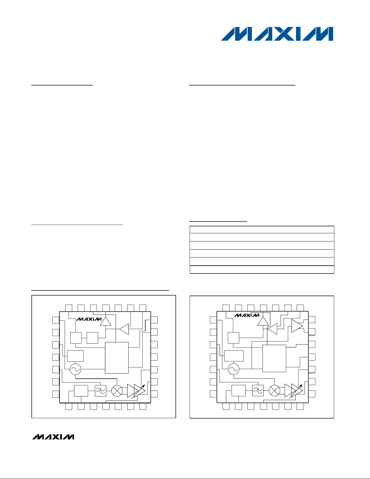
Functional Diagrams/Pin Configurations
19-2145; Rev 2; 12/07
Ordering Information
*Exposed pad
PART
TEMP RANGE
PIN-PACKAGE
MAX2900EGI -40°C to +85°C 28 QFN-EP*
MAX2901EGI -40°C to +85°C 28 QFN-EP*
MAX2902EGI -40°C to +85°C 28 QFN-EP*
MAX2903EGI -40°C to +85°C 28 QFN-EP*
MAX2904EGI -40°C to +85°C 28 QFN-EP*
Functional Diagrams/Pin Configurations are continued at end of data sheet.
For pricing, delivery, and ordering information, please contact Maxim Direct at 1-888-629-4642,
or visit Maxim’s website at www.maxim-ic.com.
VCC5
CPOUT
28
27 25 24 23 22
VTUNE
1
2
GND
3
VREG
4
VCC1
RLPF
5
6
EN
7
REFEN
MODIN
MAX2900
CP
REG
GATE
810911121314
OOKIN
REFOUT
8-CHANNEL
SYNTHESIZER
VASK
VCC4
LD
D2
26
÷4
VCC2
REFIN
PWRSET
OSC
VCC3
D0
21
D1
20
19
N.C.
18
N.C.
RF+
17
RF-
16
15
GND
Page 2
MAX2900–MAX2904
200mW Single-Chip Transmitter ICs for
868MHz/915MHz ISM Bands
2 _______________________________________________________________________________________
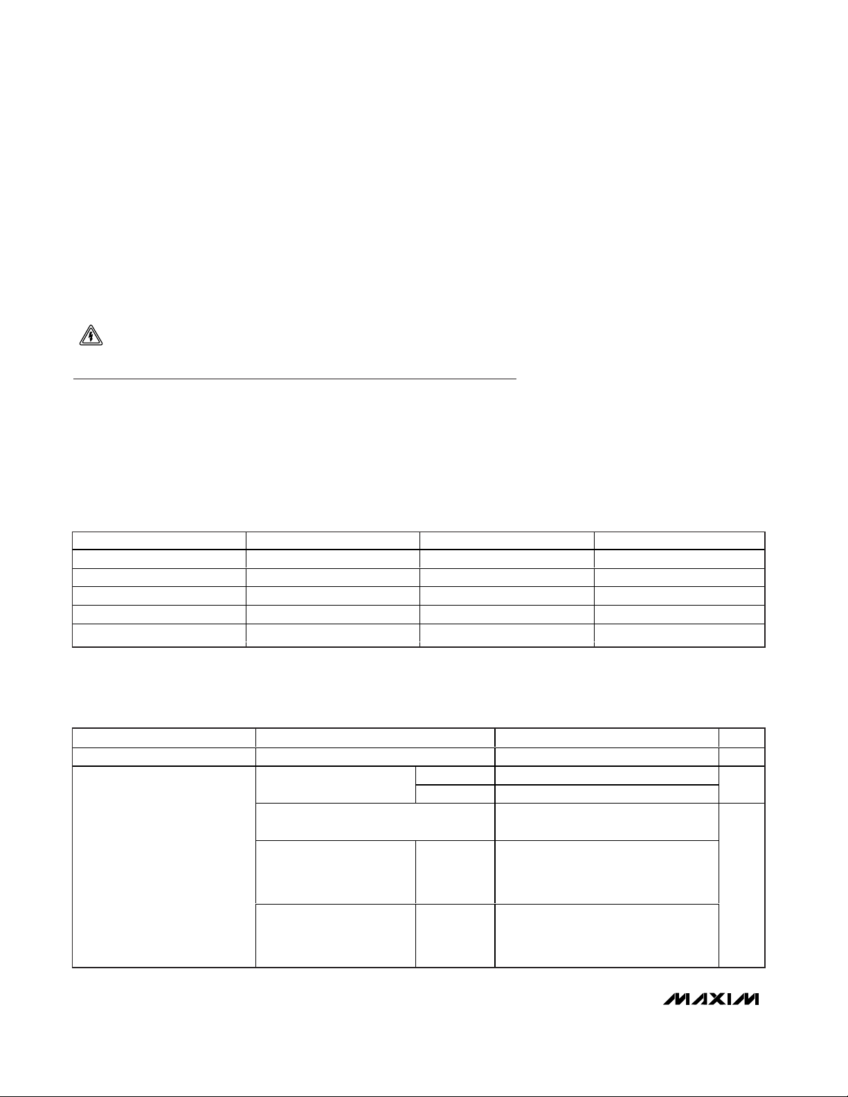
ABSOLUTE MAXIMUM RATINGS
DC ELECTRICAL CHARACTERISTICS
(VCC= +2.7V to +4.5V, EN = OOKIN = REFEN = high, TA= -40°C to +85°C. Typical values are at VCC= +4.5V, TA= +25°C, unless
otherwise noted.) (Note 1)
Stresses beyond those listed under “Absolute Maximum Ratings” may cause permanent damage to the device. These are stress ratings only, and functional
operation of the device at these or any other conditions beyond those indicated in the operational sections of the specifications is not implied. Exposure to
absolute maximum rating conditions for extended periods may affect device reliability.
VCCto GND...........................................................-0.3V to +5.0V
Analog/Digital Input Voltage to GND..........-0.3V to (V
CC
+ 0.3V)
Analog/Digital Input Current ..............................................±10µA
Continuous Power Dissipation (T
A
= +70°C)
28-Pin QFN-EP (derate 28.5mW/°C above +70°C)............2W
Operating Temperature Range ...........................-40°C to +85°C
Junction Temperature .....................................................+150°C
Storage Temperature Range .............................-65°C to +150°C
Lead Temperature (soldering, 10s) .................................+300°C
PARAMETER CONDITIONS
UNITS
Supply Voltage
4.5 V
10
Shutdown mode: EN =
REFEN = low
60
µA
Synth mode: OOKIN = low
(MAX2900/MAX2901/MAX2903 only)
32 40
Transmit mode with output
matching optimized for
+23dBm at +4.5V: PWRSET
loaded with 22kΩ resistor
T
A
= -40°C
to +85°C
Supply Current
Transmit mode with output
matching optimized for
+20dBm at +3.0V: PWRSET
loaded with 22kΩ resistor
T
A
= -40°C
to +85°C
mA
Five different versions are available. The versions differ
by their frequency band of operation, and by the synthesizer’s mode of operation. The MAX2900 has an internal
8-channel synthesizer.
The MAX2901 and MAX2903 are dual-channel versions
with a selectable internal synthesizer division ratio of 62
or 63. The MAX2901 operates in the 902MHz to
928MHz ISM band and the MAX2903 operates in the
867MHz to 870MHz European ISM band.
The MAX2902 and MAX2904 require an off-chip frequency synthesizer. The MAX2902 operates in the
902MHz– 928MHz ISM band and MAX2904 operates in
the 867MHz–870MHz European ISM band.
The MAX2901–MAX2904 provide LO outputs to drive a
receiver and/or an external synthesizer.
PART
FREQUENCY RANGE (MHz)
SYNTHESIZER LO OUTPUTS
MAX2900EGI 902 to 928
No
MAX2901EGI 902 to 928
Yes
MAX2902EGI 902 to 928 Off-chip Yes
MAX2903EGI 867 to 870
Yes
MAX2904EGI 867 to 870 Off-chip Yes
Part Selection Information
CAUTION! ESD SENSITIVE DEVICE
Internal 8 selectable channels
Internal 2 selectable channels
Internal 2 selectable channels
MIN -3σ TYP +3σ MAX
2.7 4.5
VCC = +4.0V 0.7
VCC = +4.5V
150 200
110 135
200
Page 3
MAX2900–MAX2904
200mW Single-Chip Transmitter ICs for
868MHz/915MHz ISM Bands
_______________________________________________________________________________________ 3
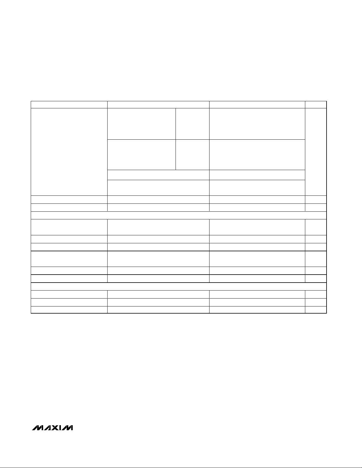
DC ELECTRICAL CHARACTERISTICS (continued)
(VCC= +2.7V to +4.5V, EN = OOKIN = REFEN = high, TA= -40°C to +85°C. Typical values are at VCC= +4.5V, TA= +25°C, unless
otherwise noted.) (Note 1)
PARAMETER CONDITIONS
MIN
-3σ
TYP
+3σ
MAX
UNITS
Transmit mode with output
matching optimized for
+17dBm at +3.0V: PWRSET
loaded with 36kΩ resistor
75
Transmit mode with output
matching optimized for
+14dBm at +3.0V: PWRSET
loaded with 51kΩ resistor
57
Reference-only mode: EN = low 2 3
Supply Current (continued)
PA standby mode: OOKIN = low
(MAX2902/MAX2904 only)
29 33
mA
VCO Input Tuning Pin Current VTUNE = +4.5V, TA = +25°C
2µA
VREG VCO Regulator Voltage
V
D IG IT A L IN PU T /O U T PU T S ( P IN S E N , RE FE N , D 0, D 1, D 2, M O D IN , O OKIN , LD )
Input Level High
V
CC
V
Input Level Low 0.5 V
Input Bias Current
10 µA
Output Level High
V
Output Level Low 0.4 V
Output Current
µA
ANALOG CONTROL INPUTS (PINS PWRSET, RLPF, VASK)
PWRSET Voltage
V
RLPF Voltage
V
VASK Input Impedance
100
220
400
kΩ
TA = +25°C
TA = +25°C
0.02
2.0
- 0.5V
-10
V
CC
- 0.4
-100 100
1.2
1.2
Page 4
MAX2900–MAX2904
200mW Single-Chip Transmitter ICs for
868MHz/915MHz ISM Bands
4 _______________________________________________________________________________________
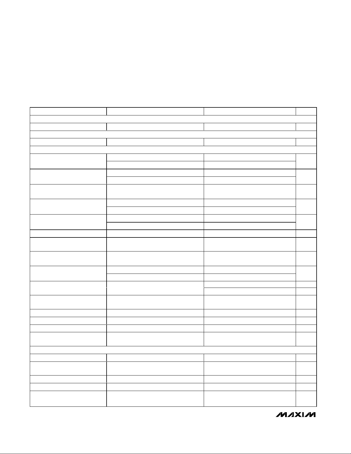
AC ELECTRICAL CHARACTERISTICS
(MAX290_ EV kits. VCC= +2.7V to +4.5V, R
RLPF
= 68kΩ, R
PWRSET
= 22kΩ, fRF= 917.28MHz (MAX2900/MAX2901/MAX2902) or f
RF
= 868MHz (MAX2903/MAX2904), VASK = VREG, f
REF
= 14.56MHz (MAX2900/MAX2901/MAX2902) or f
REF
= 13.62MHz
(MAX2903/MAX2904), chip rate on MODIN = 1.22Mbps, P
OUT
= +23dBm, TA= -40°C to +85°C. Typical values are at VCC= +4.5V,
T
A
= +25°C, unless otherwise noted.) (Note 1)
PARAMETER CONDITIONS
MIN
-3σ
TYP
+3σ
MAX
U N I T S
ANALOG INPUT PINS
VTUNE Input Capacitance VTUNE = +1.35V 15 p F
DIGITAL INPUT PINS
Digital Input Pin Capacitance 3 p F
VCO AND SYNTHESIZERS SECTION
(MAX2900/MAX2901/MAX2902)
RFOUT Frequency Range
(MAX2903/MAX2904)
M H z
(MAX2900/MAX2901/MAX2902) 14
15
REFIN Reference Frequency
Range
(MAX2903/MAX2904) 13
M H z
REFDIV Fixed Reference Divider
Ratio
(MAX2900) 4 4 4
Table 4 (MAX2900)
Main Divider Ratios
(MAX2901/MAX2903) 62 63
(MAX2900)
PLL Comparison Frequency
(MAX2901/MAX2903) 13 15
M H z
VCO Buffer Output Power
-12
d Bm
REFDIV Fixed Reference
Divider Ratio
(MAX2901/MAX2903) 1 1 1
VCO Phase Noise
At 100kHz offset, measured at RFOUT,
PLL loop BW = 5kHz
d Bc/H z
(MAX2900/MAX2901/MAX2902) 44 65 86
VCO Tuning Gain
(MAX2903/MAX2904) 85
M H z/V
kH z RM S
VCO Frequency Pulling with
OOK Modulation
OOKIN clocked at 19kHz, internal (crystal)
or external reference frequency 60
kH z p eak
PLL Phase Noise
Measured at RFOUT, 5kHz offset,
PLL loop BW = 50kHz
-96
d Bc/H z
REFOUT Voltage Swing
m V p - p
CPOUT Charge Pump Current
µA
Reference Spurs -62 d Bc
Reference Input Voltage for
Nominal Operation
Using an external frequency reference
m V
BPSK, OOK MODULATOR, AND PA
MODIN Frequency Range 1.2 8
M b /s
Modulation Filter Nominal 3dB
Bandwidth
1
M H z
Modulation Filter Final Attenuation
Measured at 30MHz 28 41 d B
Carrier Suppression 28 d B
Noise Power Density
At 960MHz (measured at RFOUT at
+23dBm output power)
d Bc/H z
300Ω d i ffer enti al l oad ( M AX 2901–M AX 2904)
902 917.28 928
867 868 870
14.56
13.78 14.5
249 256
3.5 3.64 3.75
100
200 300
-101
5
500
-150
Page 5
MAX2900–MAX2904
200mW Single-Chip Transmitter ICs for
868MHz/915MHz ISM Bands
_______________________________________________________________________________________ 5
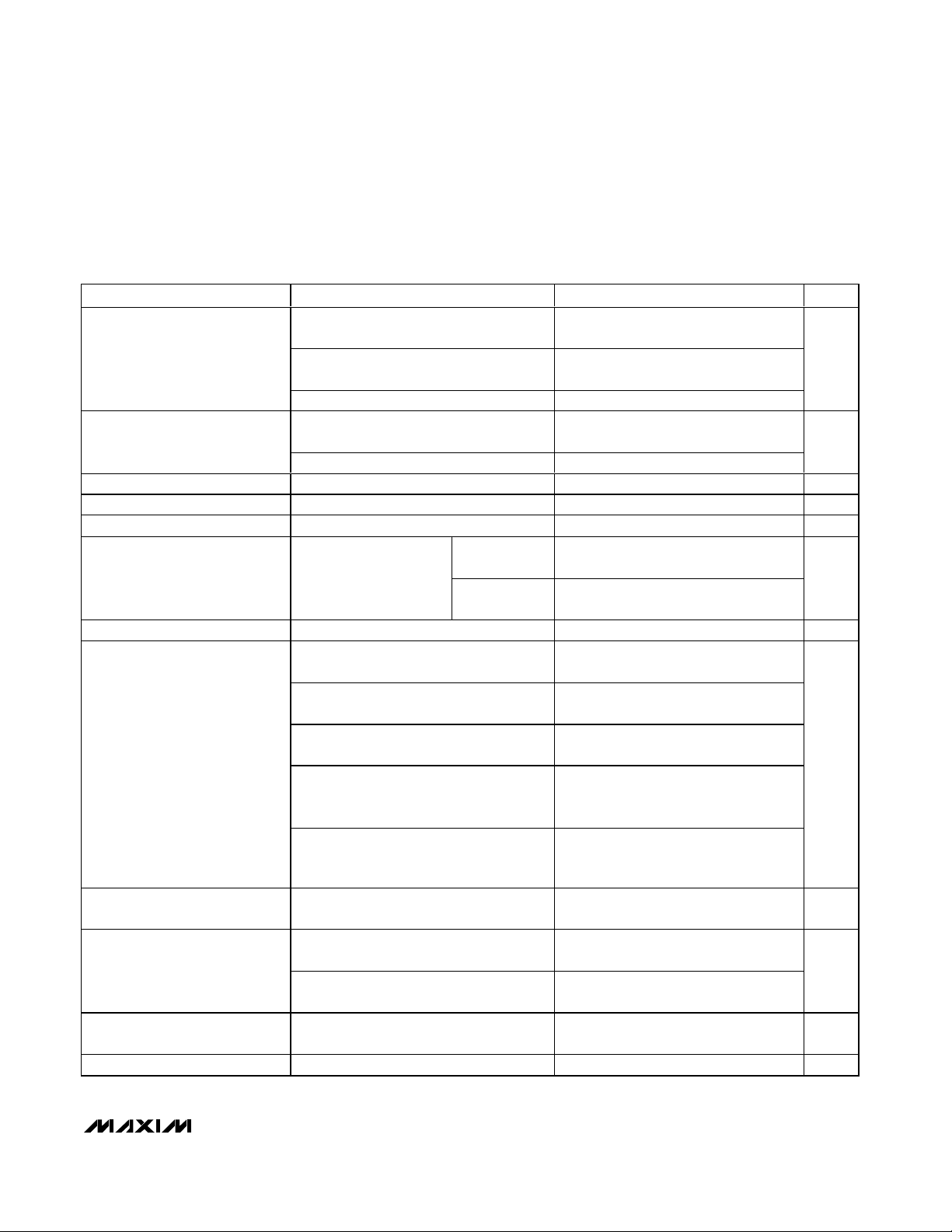
AC ELECTRICAL CHARACTERISTICS (continued)
(MAX290_ EV kits. VCC= +2.7V to +4.5V, R
RLPF
= 68kΩ, R
PWRSET
= 22kΩ, fRF= 917.28MHz (MAX2900/MAX2901/MAX2902) or f
RF
= 868MHz (MAX2903/MAX2904), VASK = VREG, f
REF
= 14.56MHz (MAX2900/MAX2901/MAX2902) or f
REF
= 13.62MHz
(MAX2903/MAX2904), chip rate on MODIN = 1.22Mbps, P
OUT
= +23dBm, TA= -40°C to +85°C. Typical values are at VCC= +4.5V,
T
A
= +25°C, unless otherwise noted.) (Note 1)
PARAMETER CONDITIONS
U N I T S
PWRSET = 22kΩ, VCC = +4.5V,
T
A
= +25°C
PWRSET = 22kΩ, VCC = +4.5V,
T
A
= -40°C to +85°C
RF Output Power
P WRS E T = 22kΩ , V
C C
= + 3.0V , TA = + 25°C
20
d Bm
fRF = 900MHz to 930MHz
(MAX2900/MAX2901/MAX2902)
0.3
RF Output Power Flatness
f
RF
= 867MHz to 870MHz
0.1
d B
Adjacent Channel Power Ratio PN sequence at 1.22MHz -17 d Bc
Alternate Channel Power Ratio PN sequence at 1.22MHz -26 d Bc
OOK Control Range 40 80 d B
OOKIN = high,
VASK = 0
41
ASK Output Power Adjustment
Range
ASK output power back-
OOKIN = high,
VASK = 1V
16
d B
RFOUT Rise and Fall Time Square-wave signal applied on OOK 1 µs
At 2nd harmonic of RF output frequency
with external matching network
-50
At 3rd harmonic of RF output frequency
with external matching network
-51
At 4th harmonic of RF output frequency
with external matching network
-63
Out of 902MHz to 928MHz band other than
harmonics with external matching network
(MAX2900/MAX2901/MAX2902)
Spurious Emissions
Out of 867MHz to 870MHz band other than
harmonics with external matching network
(MAX2903/MAX2904)
d Bc
Unlocked, Out-of-Band Spurious
Output Level
Any condition when synthesizer unlocked
(pin LD low)
d Bm
Modulation off, measured at 960MHz, any
Noise Level Out of Band
Modulation off, measured at 900MHz, any
gain setting (MAX2903/MAX2904)
d Bm /H z
Output VSWR for Guaranteed
Stability
2:1
M axi m um Al l ow ab l e Outp ut V S WR
2:1
Note 1: Devices are production tested at TA= +25°C and +85°C. Min/Max values are guaranteed by design and characterization
over temperature and supply voltage.
off relative to max power
gain setting (MAX2900/MAX2901/MAX2902)
MIN -3σ TYP +3σ MAX
21 23.5 25
20.5 25
18
< -70
< -70
< -50
-126 -120
-126 -120
21
Page 6
MAX2900–MAX2904
200mW Single-Chip Transmitter ICs for
868MHz/915MHz ISM Bands
6 _______________________________________________________________________________________
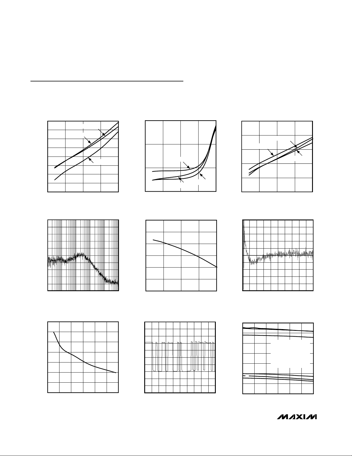
Typical Operating Characteristics
(MAX290_ EV kits. VCC= +4.5V, fRF= 917.28MHz (MAX2900/MAX2901/MAX2902) or fRF= 868MHz (MAX2903/MAX2904), R
RLPF
=
68kΩ, R
PWRSET
= 22kΩ, VASK = VREG, f
REF
= 14.56MHz (MAX2900/MAX2901/MAX2902) or f
REF
= 13.78MHz (MAX2903/MAX2904),
chip rate on MODIN = 1.22 Mbps, RF output matching network optimized for +23dBm, V
CC
= 4.5V, TA= +25°C, unless
otherwise noted.)
SUPPLY CURRENT vs. V
CC
MAX2900 toc01
VCC (V)
SUPPLY CURRENT (mA)
4.03.53.0
90
100
110
120
130
140
150
160
80
2.5 4.5
TA = +85°C
TA = +25°C
TA = -40°C
SHUTDOWN CURRENT vs. V
CC
MAX2900 toc02
VCC (V)
SHUTDOWN CURRENT (μA)
4.03.53.0
1
10
100
0.1
2.5 4.5
TA = +85°C
TA = +25°C
TA = -40°C
OUTPUT POWER vs. V
CC
MAX2900 toc03
VCC (V)
OUTPUT POWER (dBm)
4.03.53.0
18
20
22
24
26
16
2.5 4.5
TA = +85°C
TA = +25°C
TA = -40°C
VCO PHASE NOISE AT 917.28MHz
MAX2900 toc04
-40dBc/Hz
-140dBc/Hz
FREQUENCY OFFSET (MHz)
VCO SUPPLY PUSHING vs. V
CC
MAX2900 toc05
VCC (V)
OUTPUT FREQUENCY (MHz)
4.03.53.0
915.5
916.0
916.5
917.0
917.5
918.0
915.0
2.5 4.5
PLL LOCK TIME
MAX2900 toc06
100kHz
-100kHz
START 0s
20kHz/div
STOP 30μs
LOWPASS FILTER 3-dB RESPONSE
vs. R
RLPF
MAX2900 toc07
R
RLPF
(kΩ)
LOWPASS FILTER 3-dB BANDWIDTH (kHz)
6050403020
500
1000
1500
2000
2500
3000
3500
0
10 70
BPSK MODULATION OUTPUT vs. TIME
MAX2900 toc08
225deg
-225deg
45deg/div
START 0s
STOP 40μs
RF POWER vs. FREQUENCY
(MAX2900/MAX2901/MAX2902)
MAX2900 toc09
FREQUENCY (MHz)
RF POWER (dBm)
925920915910905
19
20
21
22
23
24
25
18
900 930
A
B
C
E
F
D
A: VCC = 4.5V, TA = -40°C
B: V
CC
= 4.5V, TA = +25°C
C: V
CC
= 4.5V, TA = +85°C
D: V
CC
= 2.7V, TA = -40°C
E: V
CC
= 2.7V, TA = +25°C
F: V
CC
= 2.7V, TA = +85°C
Page 7

Typical Operating Characteristics (continued)
(MAX290_ EV kits. VCC= +4.5V, fRF= 917.28MHz (MAX2900/MAX2901/MAX2902) or fRF= 868MHz (MAX2903/MAX2904), R
RLPF
=
68kΩ, R
PWRSET
= 22kΩ, VASK = VREG, f
REF
= 14.56MHz (MAX2900/MAX2901/MAX2902) or f
REF
= 13.78MHz (MAX2903/MAX2904),
chip rate on MODIN = 1.22 Mbps, RF output matching network optimized for +23dBm, V
CC
= 4.5V, TA= +25°C, unless
otherwise noted.)
MAX2900–MAX2904
200mW Single-Chip Transmitter ICs for
868MHz/915MHz ISM Bands
_______________________________________________________________________________________ 7
RF POWER vs. FREQUENCY
(MAX2903/MAX2904)
MAX2900 toc10
FREQUENCY (MHz)
RF POWER (dBm)
872868864
13
14
15
16
17
12
860 876
VCC = +3.6V
VCC = +3.0V
VCC = +2.7V
RF OUTPUT MATCHING
OPTIMIZED FOR +14dBm
OUTPUT AT V
CC
= +3.0V
OUTPUT SPECTRUM WITH 600kHz
SQUARE WAVE INPUT AT MODIN
MAX2900 toc11
30dBm
-70dBm
10dB/div
MKR
917.31MHz
-16.33dBm
CENTER 917.28MHz
SPAN 20MHz
OUTPUT SPECTRUM WITH PN SEQUENCE
AT 1.22MHz AT MODIN
MAX2900 toc12
30dBm
-70dBm
10dB/div
MKR
917.35MHz
8.17dBm
CENTER 917.28MHz
SPAN 20MHz
RF OUT RISE AND FALL TIME TRANSIENT
WITH SQUARE OOK
MAX2900 toc13
0dBVp-p
-100dBVp-p
10dB/div
T
r
T
f
START 46μs
STOP 86μs
RF OUT RISE AND FALL TIME TRANSIENT
WITH SQUARE ASK
MAX2900 toc14
22dBVp-p
-78dBVp-p
10dB/div
T
r
T
f
START 45μs
STOP 85μs
SPURIOUS LEVEL FROM
DC TO 7TH HARMONIC
MAX2900 toc15
MKR
910MHz
23.17dBm
30dBm
-70dBm
10dB/div
START 0Hz
STOP 7GHz
SPURIOUS LEVEL BETWEEN ±50MHz
FROM CARRIER FREQUENCY
MAX2900 toc16
30dBm
-70dBm
10dB/div
CENTER 917.28MHz
SPAN 100MHz
TRANSMITTER EFFICIENCY vs. R
PWRSET
MAX2900 toc17
R
PWRSET
(kΩ)
TRANSMITTER EFFICIENCY (%)
383430262218
15
20
25
30
35
40
45
10
14
A
B
C
E
F
D
A: VCC = 4.5V, TA = -40°C
B: V
CC
= 4.5V, TA = +25°C
C: V
CC
= 4.5V, TA = +85°C
D: V
CC
= 2.7V, TA = -40°C
E: V
CC
= 2.7V, TA = +25°C
F: V
CC
= 2.7V, TA = +85°C
Page 8

MAX2900–MAX2904
200mW Single-Chip Transmitter ICs for
868MHz/915MHz ISM Bands
8 _______________________________________________________________________________________
Pin Description
PIN
MAX2900
MAX2901
MAX2903
MAX2902
MAX2904
NAME PIN TYPE FUNCTION
1 1 1 VTUNE Analog Input VCO tuning voltage input
2 2 2 GND Supply Pin Ground
3 3 3 VREG
Analog
Input/Output
Regulated voltage output to supply the VCO.
Bypass with a 0.01µF capacitor to GND as
close to the part as possible.
4 4 4 VCC1 Supply Pin
Power supply pin for VCO circuits. Bypass
with a 1000pF and a 10µF capacitor to GND
as close to the part as possible.
5 5 5 RLPF
Analog Input
Resistor to ground on this pin sets the
modulation filter bandwidth.
6 6 6 EN Digital Input
Chip-enable digital input pin. Set EN low
maintain the chip in power-down mode.
7 7 7 REFEN Digital Input
Enable for crystal oscillator and frequency
reference buffer.
8 8 8 MODIN Digital Input BPSK modulation input
9 9 9 OOKIN Digital Input On-off keying modulation. On state = high.
10 10 10 VCC2 Supply
Power supply pin for internal RF buffer
circuits. Bypass with a 100pF and a 0.01µF
capacitor to GND as close to the part as
possible.
11 11 11 VASK
Analog Voltage
Input
ASK voltage input pin
12 12 — LD
Lock detector output digital pin. Level is
high when PLL is inside lock range.
— — 12 D.C.
—
13 13 13 PWRSET
Anal og Inp ut
Current input set to adjust output power.
14 14 14 VCC3 Supply
P ow er sup p l y p i n for RF p ow er am p l i fi er
ci r cui ts. Byp ass w i th a 100p F cap aci tor to GN D
as cl ose to the p ar t as p ossi b l e.
Resistor to Ground
Digital Output
Do NOT Connect
Resi stor to Gr ound
Page 9

MAX2900–MAX2904
200mW Single-Chip Transmitter ICs for
868MHz/915MHz ISM Bands
_______________________________________________________________________________________ 9
Pin Description (continued)
PIN
MAX2900
MAX2901
MAX2903
MAX2902
MAX2904
NAME PIN TYPE FUNCTION
15 15 15 GND Supply Pin Ground
16, 17 16, 17 16, 17 RF-, RF+ RF Output RF d i ffer enti al outp ut, op en- col l ector typ e
18 — — N.C.
—
— 18 — GND Supply Pin Ground
— — 18 D.C.
—
19 — 19 N.C.
—
— 19 — DIVOUT ECL Output Divider output
— 20, 21 20, 21 VCO-, VCO+
Open Collector
RF
VCO output (differential)
20 — — D1 Digital Input Channel selection bit 1
21 — — D0 Digital Input Channel selection bit 0
22 22 22 OSC Analog Input
Crystal oscillator connection. See Typical
Operating Circuit.
23 23 23 REFIN
Analog Voltage
Input
Refer ence i np ut p i n anal og ( can b e used as
i np ut or as cr ystal osci l l ator d r i ver ) . See
Typical Operating Circuit.
24 24 — VCC4 Supply Pin
Power-supply pin for the synthesizer circuits.
Bypass with a 1000pF capacitor to GND as
close to the part as possible.
— — 24 VCC4 Supply Pin
Power-supply pin for the digital circuits.
Bypass with a 100pF capacitor to GND as
close to the part as possible.
25 25 25 REFOUT
Buffered clock analog output pin
26 — — D2 Digital Input Channel selection bit 2
— 26 — DIV63 Digital Input
Division ratio selections (division ratio = 62
when DIV63 = high; division
ratio = 63 when DIV63 = low).
— — 26 N.C.
—
27 27 — VCC5 Supply Pin
Power-supply pin for charge pump circuits.
Bypass with a 100pF capacitor to GND as
close to the part as possible.
— — 27 VCC5 Supply Pin
Power-supply pin. Bypass with a 100pF
capacitor to GND as close to the part as
possible.
28 28 — CPOUT
Charge pump output pin
— — 28 D.C.
—
GROUND GROUND GROUND GROUND
Electrical
Ground
Back side of package is connected to
ground.
Not Connected
Do Not Connect
Not Connected
Analog Output
Not Connected
Analog Output
Do Not Connect
Page 10

Detailed Description
Principles of Operation
When EN goes high, the reference and the VCO start
while the PA stays in the off mode. For MAX2900/
MAX2901/MAX2903, the PLL also starts when EN goes
high. After the lock-detect pin LD goes high, the PA is set
to stand-by mode. For the MAX2902/MAX2904, the VCO
loop has to be closed by using an external synthesizer.
After this, pulling OOKIN high turns on the PA. The internal modulation filter smoothes the power ramp-up of the
PA.
The modulation filter BW is typically 0.8MHz, used for a
1.22Mbps chip rate, and can be adjusted by varying
RLPF. A high value can be used for RLPF to get a slow
PA ramping up when BPSK is not used.
The reference blocks can be turned on separately (and
earlier) by pulling REFEN high, to allow the crystal frequency to settle.
The device supports various modulation modes:
• BPSK, filtered by the internal modulation filter, is
obtained through the MODIN pin. This is the preferred mode of operation for MAX2900.
• OOK is obtained digitally with the OOKIN pin.
• ASK is obtained through the ASK pin.
• FM is imposed on the VCO or the reference.
• FM is the preferred mode of operation for the
MAX2903/MAX2904 due to the narrowband operation common in Europe.
The maximum output power is set by the output matching network and the external biasing resistor on the
PWRSET pin.
For the MAX2901–MAX2904, differential LO outputs are
provided to drive a companion receiver and/or an
external synthesizer.
Power-Up Modes
The circuit has four modes of operations, defined as
follows:
1) Shutdown mode: Pin EN and REFEN are low, all
functions are off, and the current consumption is
leakage only.
2) Synth mode: Pin EN and REFEN are high, pin
OOKIN is low. The reference circuits, VCO, and
synthesizer are turned on. The power amplifier is in
stand-by mode. Total current is less than 50mA.
Note that as long as the LD pin is not going high,
indicating that the PLL is unlocked, OOKIN high is
ignored.
3) Transmit mode: Pin EN and REFEN are high. If output
pin LD is high, the device is ready to transmit. When
OOKIN is high, the power amplifier is turned on. The
current consumption varies between 50mA and
120mA, depending on the output power requested by
the combination of the OOK duty cycle, the PWRSET
value, and output matching circuit.
4) Reference Only mode: This mode enables the use
of the crystal reference from the IC to drive the
external logic ICs. To obtain this mode, set the
REFEN pin high and EN low. In this mode, only the
reference circuit turns on, the crystal oscillator starts,
and the clock is present at the REFOUT pin. The current consumption remains much lower than that in the
SYNTH mode because the VCO, synthesizer, and PA
standby circuits are off. When EN goes high, the IC
goes into the SYNTH mode.
Synthesizer Programming
The three pins D0–D2 (MAX2900) and DIV63 (MAX2901/
MAX2903) are used as digital entries to program the synthesizer division ratios. Tables 4 and 5 show the division
ratios obtained for the various pin logic levels.
Analog Input Control Pins
The two pins PWRSET and VASK are analog inputs
used to control the power of the transmitter. The equivalent input schematics are defined in Figures 1, 2, and
3. The PWRSET pin sets the biasing of the amplification
chain. Because the last stage of the amplifier operates
in saturation, the output power mostly depends on the
load and supply voltage. The purpose of the PWRSET
resistor is to achieve optimum biasing (and therefore
efficiency) for various maximum output power configurations. For a given application with a known operating
voltage and peak power, a fixed value of resistor is
determined. The output power range of -7dBm to
+23dBm at 4.5V is obtained by choosing a combination
of output load line and the resistor on PWRSET; 22kΩ is
MAX2900–MAX2904
200mW Single-Chip Transmitter ICs for
868MHz/915MHz ISM Bands
10 ______________________________________________________________________________________
1.2V
100Ω
INTERNAL
CIRCUITS
PIN PWRSET
EXTERNAL
RESISTOR
TO INTERNAL
CONTROL
CIRCUIT
Figure 1. PIN PWRSET Equivalent Circuit
Page 11

MAX2900–MAX2904
200mW Single-Chip Transmitter ICs for
868MHz/915MHz ISM Bands
______________________________________________________________________________________ 11
used on the EV kit board for +23dBm output power at
4.5V, and 22kΩ is also recommended for +20dBm output power at +3.0V. For +17dBm at 3.0V, 36kΩ is recommended. The current consumption, efficiency, and
distortion in the amplification chain are affected by the
choice of the resistor RPWRSET, offering a lot of design
flexibility.
The VASK pin is an input to the internal gain control circuitry. The gain control is greater than 30dB over the
full range of input voltages from 0 to VREG = 2.1V. This
input is used for ASK modulation. At 1V, a typical 15dB
attenuation is obtained from the peak power. When this
input is not used, connect VASK to VREG.
The RLPF input controls the modulation filter center frequency.
The RLPF pin sets the bandwidth of the modulation filter. The default filter bandwidth, obtained with a 68kΩ
resistor, is for 1.2Mchips/s. The bandwidth is increased
to accommodate 5Mchips/s by decreasing the resistor
value to about 26kΩ. The minimum value for the resistor
is 12kΩ, which generates the maximum filter bandwidth. A higher value can be used in FM mode to set
up a slow ramp-up time for the PA.
Data Filter Characteristics
The data filter approximates a 3rd-order Butterworth filter. The 3dB cut-off frequency is adjusted through the
resistor on pin RLPF, which controls the first two poles
of the filter (the last high-frequency pole is fixed and set
around 10MHz). The filter is adjustable in a range from
approximately 700kHz to 7MHz.
With the nominal setting (3dB cut off at 0.8MHz), the filter attenuation is 10dB at 3.6MHz. If used with a BPSK
at 1.22MHz, this provides about 30dB of modulation
rolloff at 3.6MHz. Hence, a significant channelization
effect is obtained.
In the wideband setting (3dB cut off at 5MHz), the
attenuation at 30MHz is still 30dB, helping to pass the
FCC spurious emissions at 960MHz.
1.2V
100Ω
INTERNAL
CIRCUITS
PIN RLPF
EXTERNAL
RESISTOR
TO INTERNAL
CONTROL
CIRCUIT
Figure 2. PIN VASK Equivalent Circuit
Figure 3. PIN RLPF Equivalent Circuit
TO VREG
(2.1V)
TO INTERNAL
CONTROL
CIRCUIT
>200kΩ
1.5V
INTERNAL
CIRCUITS
PIN
VASK
EXTERNAL
RESISTOR
BRIDGE
Page 12

MAX2900–MAX2904
200mW Single-Chip Transmitter ICs for
868MHz/915MHz ISM Bands
12 ______________________________________________________________________________________
Table 2. MAX2901/MAX2903 Power-Up Modes
Table 3. MAX2902/MAX2904 Power-Up Modes
Table 4. MAX2900 Synthesizer
Programming
REFEN
EN
OOKIN
REFERENCE
VCO MOD FILTER
SYNTHESIZER PA
0 0 X Off Off Off Off
1 0 X On Off Off Off
1 1 0 On On On Off
111 On On On
On only after LD
goes high
Table 5. MAX2901/MAX2903 Synthesizer
Programming
DIV 63 DIVISION RATIO
062
163
Table 1. MAX2900 Power-Up Modes
LOGIC LEVEL INTERNAL BLOCK STATUS
EN
REFERENCE
SYNTHESIZER PA
0 0 X Off Off Off Off
1 0 X On Off Off Off
1 1 0 On On On Off
1 1 1 On On On
On only after LD
goes high
REFEN
OOKIN
REFEN EN OOKIN REFERENCE VCO MOD FILTER PA
0 0 X Off Off Off
1 0 0 On Off Off
0 1 0 Off On Off
1 1 0 On On Off
0 1 1 Off On On
111 On On On
VCO MOD FILTER
D0 D1 D2 DIVISION RATIO
0 1 1 249
0 1 0 250
0 0 1 251
0 0 0 252
1 1 1 253
1 1 0 254
1 0 1 255
1 0 0 256
Page 13

MAX2900–MAX2904
200mW Single-Chip Transmitter ICs for
868MHz/915MHz ISM Bands
______________________________________________________________________________________ 13
1
3
2
4
5
6
7
211920
18
17
16
15
810911121314
28
2627 25 24 23 22
REFEN
EN
RLPF
R5
VCC1
VREG
GND
WBFM
(OPT)
VTUNE
GND
C8
R7 R8
ASK
(OPT)
R6
RF-
RF+
N.C.
N.C.
D1
D0
D1
D0
OSC
REFIN
VCC4
REFOUT
REFOUT
D2
VCC5
CPOUT
VCC3
PWRSET
LD
VASK
VREG
VCC2
OOKIN
OOK
MODIN
MODIN (PN)
VCC_PA
C26
C23
Y1 (OPT)
C25
C24
C15
C16
L3
L1
L5
LOOP
ANTENNA
C31
C33
C28
C18
VCC_DRV
C4
C2
C1 C35
C3
R4
R3 R1
EXT REFERENCE (OPT)
L4
L2
C32
C34
8-CHANNEL
SYNTHESIZER
CP
GATE
REG
÷4
MAX2900
MAX2900 TYPICAL OPERATING CIRCUIT
C12
C13
Typical Operating Circuits
Page 14

MAX2900–MAX2904
200mW Single-Chip Transmitter ICs for
868MHz/915MHz ISM Bands
14 ______________________________________________________________________________________
1
3
2
4
5
6
7
211920
18
17
16
15
810911121314
28
2627 25 24 23 22
REFEN
EN
RLPF
C13
R5
VCC1
VREG
GND
WBFM
(OPT)
VTUNE
GND
C8
R7 R8
ASK
(OPT)
R6
RF-
RF+
GND
DIVOUT
VCO-
VCO+
OSC
REFIN
VCC4
REFOUT
REFOUT
R11
VCC5
CPOUT
VCC3
PWRSET
LD
VASK
VREG
VCC2
OOKIN
OOK
MODIN
MODIN (PN)
R10
VCC
C37
VCOOUT
VCC_PA
C26
C23
Y1
C25
C24
C15
C16
C12
L3
L1
L5
LOOP
ANTENNA
C31
C33
C28
C18
VCC_DRV
C4
C2
C1 C35
C3
R4
R3 R1
EXT REFERENCE
/FM INPUT
L4
L2
C32
C34
DUAL-
CHANNEL
(/62 OR /63)
SYNTHESIZER
CP
GATE
REG
MAX2901/
MAX2903
MAX2901/MAX2903 TYPICAL OPERATING CIRCUIT
DIV63
Typical Operating Circuits (continued)
Page 15

MAX2900–MAX2904
200mW Single-Chip Transmitter ICs for
868MHz/915MHz ISM Bands
______________________________________________________________________________________ 15
1
3
2
4
5
6
7
211920
18
17
16
15
810911121314
28
2627 25 24 23 22
REFEN
EN
RLPF
C13
R5
VCC1
VREG
GND
WBFM
(OPT)
VTUNE
GND
C8
R7 R8
ASK
(OPT)
R6
RF-
RF+
D.C.
N.C.
VCO-
VCO+
OSC
REFIN
VCC4
REFOUT
R11
N.C.
VCC5
D.C.
VCC3
PWRSET
D.C.
VASK
VREG
VCC2
OOKIN
OOK
MODIN
MODIN (PN)
GATE
REG
MAX2902/
MAX2904
R10
VCC
CPOUT
REFIN
1GHz
FREQUENCY
SYNTH
RFIN
C37
VCOOUT
VCC_PA
C26
C15
C16
C12
L3
L1
L5
LOOP
ANTENNA
C31
C33
C28
C18
VCC_DRV
C4
C2
C1 C35
C3
R4
R3 R1
REFFREQ
/FM
L4
L2
C32
C34
MAX2902/MAX2904 TYPICAL OPERATING CIRCUIT
Typical Operating Circuits (continued)
Page 16

MAX2900–MAX2904
200mW Single-Chip Transmitter ICs for
868MHz/915MHz ISM Bands
16 ______________________________________________________________________________________
1
3
2
4
5
6
7
21
19
20
18
17
16
15
810911121314
28
2627 25 24 23 22
REFEN
EN
RLPF
VCC1
VREG
GND
VTUNE
RF-
RF+
D.C.
N.C.
VCO-
VCO+
OSC
REFIN
VCC4
REFOUT
N.C.
VCC5
D.C.
VCC3
PWRSET
D.C.
VASK
VCC2
OOKIN
MODIN
GATE
REG
MAX2902/
MAX2904
GND
Functional Diagrams/
Pin Configurations (continued)
Chip Information
TRANSISTOR COUNT: 898
Page 17

MAX2900–MAX2904
200mW Single-Chip Transmitter ICs for
868MHz/915MHz ISM Bands
______________________________________________________________________________________ 17
32L QFN.EPS
Package Information
(The package drawing(s) in this data sheet may not reflect the most current specifications. For the latest package outline information
go to www.maxim-ic.com/packages
.)
Page 18

200mW Single-Chip Transmitter ICs for
868MHz/915MHz ISM Bands
Package Information (continued)
(The package drawing(s) in this data sheet may not reflect the most current specifications. For the latest package outline information
www.maxim-ic.com/packages
go to
.)
MAX2900–MAX2904
18 ______________________________________________________________________________________
Page 19

200mW Single-Chip Transmitter ICs for
868MHz/915MHz ISM Bands
Maxim cannot assume responsibility for use of any circuitry other than circuitry entirely embodied in a Maxim product. No circuit patent licenses are
implied. Maxim reserves the right to change the circuitry and specifications without notice at any time.
Maxim Integrated Products, 120 San Gabriel Drive, Sunnyvale, CA 94086 408-737-7600 ____________________ 19
© 2007 Maxim Integrated Products Printed USA is a registered trademark of Maxim Integrated Products, Inc.
Revision History
REVISION
NUMBER
REVISION
DATE
DESCRIPTION
PAGES
CHANGED
18/03— —
2 12/07 Separate VCO Tuning Gain specification into two rows 4
 Loading...