


General Description
The MAX2839AS direct conversion, zero-IF, RF transceiver
is designed specifically for 2.3GHz to 2.7GHz 802.16e
MIMO mobile WiMAX™ systems. The device incorporates one transmitter and two receivers, with > 40dB isolation between each receiver. The MAX2839AS
completely integrates all circuitry required to implement
the RF transceiver function, providing RF to baseband
receive path, and baseband to RF transmit path, VCO,
frequency synthesizer, crystal oscillator, and baseband/control interface. The device includes a fast-settling sigma-delta RF synthesizer with smaller than 40Hz
frequency steps and a crystal oscillator that allows the
use of a low-cost crystal in place of a TCXO. The transceiver IC also integrates circuits for on-chip DC-offset
cancellation, I/Q error, and carrier leakage detection
circuits. An internal transmit to receive loopback mode
allows for receiver I/Q imbalance calibration. The local
oscillator I/Q quadrature phase error can be digitally
corrected in approximately 0.125° steps. Only an RF
bandpass filter (BPF), crystal, RF switch, PA, and a
small number of passive components are needed to
form a complete wireless broadband RF radio solution.
The MAX2839AS completely eliminates the need for an
external SAW filter by implementing on-chip programmable monolithic filters for both the receiver and transmitter, for all 2GHz and 802.16e profiles and WiBro. The
baseband filters along with the Rx and Tx signal paths
are optimized to meet the stringent noise figure and linearity specifications. The device supports up to 2048
FFT OFDM and implements programmable channel filters for 3.5MHz to 20MHz RF channel bandwidths. The
transceiver requires only 2µs Tx-Rx switching time. The
IC is available in a small wafer-level package (WLP)
measuring 5.16mm x 3.66mm x 0.5mm.
Applications
802.16e Mobile WiMAX Systems
Korean WiBro Systems
Proprietary Wireless Broadband Systems
802.11g or n WLAN with MRC or MIMO Down Link
Features
o 2.3GHz to 2.7GHz Wideband Operation
o Dual Receivers for MIMO, Single Transmitter
o Complete RF Transceiver, PA Driver, and Crystal
Oscillator
3.5dB Rx Noise Figure on Each Receiver with
Balun
-35dB Rx EVM for 64QAM Signal
0dBm Linear OFDM Transmit Power (64QAM)
-70dBr Tx Spectral Emission Mask
-35dBc LO Leakage
Automatic Rx DC Offset Correction
Monolithic Low-Noise VCO with -39dBc
Integrated Phase Noise
Programmable Rx I/Q Lowpass Channel Filters
Programmable Tx I/Q Lowpass Anti-Aliasing
Filters
Sigma-Delta Fractional-N PLL with 28.61Hz
Minimum Step Size
62dB Tx Gain Control Range with 1dB Step
Size, Digitally Controlled
95dB Rx Gain Control Range with 1dB Step
Size, Digitally Controlled
60dB Analog RSSI Instantaneous Dynamic
Range
4-Wire SPI™ Digital Interface
I/Q Analog Baseband Interface
Digital Tx/Rx Mode Control
Digitally Tuned Crystal Oscillator
On-Chip Digital Temperature Sensor Readout
o +2.7V to +3.6V Transceiver Supply
o Low-Power Shutdown Current
o Small WLP Package (5.16mm x 3.66mm x 0.5mm)
MAX2839AS
2.3GHz to 2.7GHz MIMO Wireless
Broadband RF Transceiver
________________________________________________________________
Maxim Integrated Products
1
19-4588; Rev 1; 5/10
For pricing, delivery, and ordering information, please contact Maxim Direct at 1-888-629-4642,
or visit Maxim’s website at www.maxim-ic.com.
EVALUATION KIT
AVAILABLE
WiMAX is a trademark of the WiMAX Forum.
SPI is a trademark of Motorola, Inc.
Ordering Information
+
Denotes a lead(Pb)-free/RoHS-compliant package.
T = Tape and reel.
Bump Configuration and Typical Operating Circuit appear at
end of data sheet.
PART TEMP RANGE PIN-PACKAGE
MAX2839ASEWO+T
-40°C to +85°C 73 WLP
MAX2839AS
2.3GHz to 2.7GHz MIMO Wireless
Broadband RF Transceiver
2 _______________________________________________________________________________________
DC ELECTRICAL CHARACTERISTICS
(MAX2839AS Evaluation Kit. Unless otherwise noted, VCC_ = 2.7V to 3.6V, TA= -40°C to +85°C, Rx set to the maximum gain.
ENABLE and TXRX set according to operating mode. CS = high, SCLK = DIN = low, no input signal at RF inputs, all RF inputs and
outputs terminated into 50Ω. 90mV
RMS
differential I and Q signals (1MHz) applied to I, Q baseband inputs of transmitter in transmit
mode, all registers set to recommended settings. Typical values are at V
CC_
= 2.8V, fLO= 2.5GHz, and TA= +25°C.) (Note 2)
Stresses beyond those listed under “Absolute Maximum Ratings” may cause permanent damage to the device. These are stress ratings only, and functional
operation of the device at these or any other conditions beyond those indicated in the operational sections of the specifications is not implied. Exposure to
absolute maximum rating conditions for extended periods may affect device reliability.
ABSOLUTE MAXIMUM RATINGS
V
CC_
Pins to GND..................................................-0.3V to +3.9V
RF Inputs: RXINA+, RXINA-, RXINB+,
RXINB- to GND ............................................AC-Coupled Only
RF Outputs: TXOUT+, TXOUT- to GND.................-0.3V to +3.9V
Analog Inputs: TXBBI+, TXBBI-, TXBBQ+,
TXBBQ- to GND.................................................-0.3V to +3.9V
Analog Input: REFCLK, XTAL1 .........................-0.3V to +3.9V
P-P
Analog Outputs: RXBBIA+, RXBBIA-, RXBBQA+, RXBBQA-,
RXBBIB+, RXBBIB-, RXBBQB+, RXBBQB-, CPOUT+,
CPOUT-, PABIAS, RSSI to GND........................-0.3V to +3.9V
Digital Inputs: TXRX, CS, SCLK, DIN, B7:B0,
CLKOUT_DIV, RXHP, ENABLE to GND ............-0.3V to +3.9V
Digital Outputs: DOUT, CLKOUT ..........................-0.3V to +3.9V
Bias Voltages: VCOBYP .......................................-0.3V to +3.9V
Short-Circuit Duration on All Output Pins ...............................10s
RF Input Power: All RXIN_ ..............................................+10dBm
RF Output Differential Load VSWR: All TXOUT .......................6:1
Continuous Power Dissipation (T
A
= +70°C)
73-Bump WLP (derate 31.3mW/°C above +70°C).....2500mW
Operating Temperature Range ...........................-40°C to +85°C
Junction Temperature......................................................+150°C
Storage Temperature Range .............................-65°C to +160°C
Soldering Temperature (reflow) .........................(Note 1) +260°C
Note 1: Refer to Application Note 1891:
Understanding the Basics of the Wafer-Level Chip-Scale Package (WL-CSP)
available at
www.maxim-ic.com
.
CAUTION! ESD SENSITIVE DEVICE
Supply Voltage VCC_ 2.7 3.6 V
Supply Current
Rx I/Q Output Common-Mode
Voltage
Tx Baseband Input CommonMode Voltage Operating Range
Tx Baseband Input Bias Current Source current 10 20 µA
LOGIC INPUTS: TXRX, ENABLE, SCLK, DIN, CS, B7:B0, CLKOUT_DIV, RXHP
Digital Input-Voltage High, V
Digital Input-Voltage Low, V
Digital Input-Current High, I
PARAMETER CONDITIONS MIN TYP MAX UNITS
IH
IL
IH
Shutdown mode, T
V
CC
Clock-out only mode 2.7 3.8
Standby mode 33 50
Rx mode
Tx mode
Rx calibration mode, both receivers on 153 200
Tx calibration mode 102 145
D[9:8] = 00 in A[4:0] = 00100 0.8 1.05 1.35
D[9:8] = 01 in A[4:0] = 00100 1.15
D[9:8] = 10 in A[4:0] = 00100 1.25
D[9:8] = 11 in A[4:0] = 00100 1.45
DC-coupled 0.5 1.2 V
= +25°C; all logic inputs equal 0 or
A
One receiver on 79 101
Both receivers on 120 148
16 QAM 116 148
64 QAM (Note 3) 145 183
2µA
VCC - 0.4 V
0.4 V
-1 +1 µA
mA
V
MAX2839AS
2.3GHz to 2.7GHz MIMO Wireless
BroadbandRF Transceiver
_______________________________________________________________________________________ 3
DC ELECTRICAL CHARACTERISTICS (continued)
(MAX2839AS Evaluation Kit. Unless otherwise noted, VCC_ = 2.7V to 3.6V, TA= -40°C to +85°C, Rx set to the maximum gain.
ENABLE and TXRX set according to operating mode. CS = high, SCLK = DIN = low, no input signal at RF inputs, all RF inputs and
outputs terminated into 50Ω. 90mV
RMS
differential I and Q signals (1MHz) applied to I, Q baseband inputs of transmitter in transmit
mode, all registers set to recommended settings. Typical values are at V
CC_
= 2.8V, fLO= 2.5GHz, and TA= +25°C.) (Note 2)
AC ELECTRICAL CHARACTERISTICS—Rx MODE
(MAX2839AS Evaluation Kit. Unless otherwise noted, V
CC_
= 2.8V, TA= +25°C, fRF= 2.4999GHz, fLO= 2.5GHz; baseband output
signal frequency = 100kHz, f
REF
= 40MHz, ENABLE = TXRX = CS = high, SCLK = DIN = low, with power matching for the differential
RF pins using the
Typical Operating Circuit
and registers set to default settings. Lowpass filter is set to 10MHz RF channel BW.
Unmodulated single-tone RF input signal is used.) (Note 2)
PARAMETER CONDITIONS MIN TYP MAX UNITS
Digital Input-Current Low, I
LOGIC OUTPUTS: DOUT, CLKOUT
Digital Output-Voltage High, V
Digital Output-Voltage Low, V
IL
OH
OL
Sourcing 100µA VCC - 0.4 V
Sinking 100µA 0.4 V
-1 +1 µA
RF INPUT TO I, Q BASEBAND-LOADED OUTPUT
RF Input Frequency Range 2.3 2.7 GHz
Peak-to-Peak Gain Variation over
RF Input Frequency Range
RF Input Return Loss All LNA settings 12 dB
Total Voltage Gain
RF Gain Steps
Gain Change Settling Time
Baseband Gain Range
Baseband Gain Step Size 1dB
DSB Noise Figure
(Including Balun Loss)
PARAMETER CONDITIONS MIN TYP MAX UNITS
Tested at band edges and band center 1.5 dB
T
+85°C
From max RF gain (B7:B6 = 00) to max RF gain - 8dB
(B7:B6 = 01)
From max RF gain to max RF gain - 16dB (B7:B6 = 10) 16
From max RF gain to max RF gain - 32dB (B7:B6 = 11) 32
Any RF or baseband gain change; gain settling to within
±1dB of steady state; RXHP = 1
Any RF or baseband gain change; gain settling to within
±0.1dB of steady state; RXHP = 1
From maximum baseband gain (B5:B0 = 000000) to
minimum gain (B5:B0 = 111111), T
Voltage gain = 65dB with max RF gain (B7:B6 = 00) 3.5
V ol tag e g ai n = 50d B w i th m ax RF g ai n - 8d B ( B7:B6 = 01) 8.5
Voltage gain = 45dB with max RF gain - 16dB
(B7:B6 = 10)
Voltage gain = 15dB with max RF gain - 32dB
(B7:B6 = 11)
= -40°C to
A
Maximum gain, B7:B0 = 0000000 92 99
Minimum gain, B7:B0 = 1111111 4 10
8
200
2000
= -40°C to +85°C
A
60.5 63 65.5 dB
14.5
32
dB
dB
ns
dB
MAX2839AS
2.3GHz to 2.7GHz MIMO Wireless
Broadband RF Transceiver
4 _______________________________________________________________________________________
AC ELECTRICAL CHARACTERISTICS—Rx MODE (continued)
(MAX2839AS Evaluation Kit. Unless otherwise noted, V
CC_
= 2.8V, TA= +25°C, fRF= 2.4999GHz, fLO= 2.5GHz; baseband output
signal frequency = 100kHz, f
REF
= 40MHz, ENABLE = TXRX = CS = high, SCLK = DIN = low, with power matching for the differential
RF pins using the
Typical Operating Circuit
and registers set to default settings. Lowpass filter is set to 10MHz RF channel BW.
Unmodulated single-tone RF input signal is used.) (Note 2)
Out-of-Band Input IP3 (Note 4)
PARAMETER CONDITIONS MIN TYP MAX UNITS
Inband Input P-1dB
Maximum Output Signal Level
I/Q Gain Imbalance 100kHz IQ baseband output; 1 σ variation 0.05 dB
I/Q Phase Error 100kHz IQ baseband output; 1 σ variation 0.25 Degrees
Rx I/Q Output Load Impedance
(R || C)
Loopback Gain (for Receiver I/Q
Calibration)
AGC set for -65dBm wanted signal, max RF gain
(B7:B6 = 00)
AGC set for -55dBm wanted signal, max RF gain - 8dB
(B7:B6 = 01)
AGC set for -40dBm wanted signal, max RF gain - 16dB
(B7:B6 = 10)
AGC set for -30dBm wanted signal, max RF gain - 32dB
(B7:B6 = 11)
Max RF gain (B7:B6 = 00) -37
Max RF gain - 8dB (B7:B6 = 01) -29
Max RF gain - 16dB (B7:B6 = 01) -21
Max RF gain - 32dB (B7:B6 = 11) -4
Over passband frequency range at VGA gain between
max and max - 54dB; 1dB compression point
Minimum differential resistance 10 kΩ
Maximum differential capacitance 5 pF
Transmitter I/Q input to receiver I/Q output; transmitter
B6:B1 = 000011, receiver B5:B0 = 101010 programmed
through SPI
-13
-9
-7
+16
1.15 V
-6 -1 +4.5 dB
dBm
dBm
P-P
After switching RXHP to 0; average over 1µs after any
I/Q Output DC Droop
I/Q Static DC Offset
Isolation Between Rx Channels A
and B
RECEIVER BASEBAND FILTERS
Baseband Filter Rejection
Baseband Highpass Filter Corner
Frequency
gain change, or 2µs after receive enabled with 100Hz
AC-coupling
No RF input signal; measure at 3µs after receive enable;
RXHP = 1 for 0 to 2µs and set to 0 after 2µs, 1 σ variation
Any RF gain settings 40 dB
At 15MHz 57
At 20MHz 75
At > 40MHz 75
RXHP = 1 (used before AGC completion) 650
D[5:4] = 00 0.1
RXHP = 0 (used after AGC
completion) address A[4:0] = 01110
D[5:4] = 01 1
D[5:4] = 10 30
D[5:4] = 11 100
1 V/s
1mV
dB
kHz
MAX2839AS
2.3GHz to 2.7GHz MIMO Wireless
BroadbandRF Transceiver
_______________________________________________________________________________________ 5
AC ELECTRICAL CHARACTERISTICS—Rx MODE (continued)
(MAX2839AS Evaluation Kit. Unless otherwise noted, V
CC_
= 2.8V, TA= +25°C, fRF= 2.4999GHz, fLO= 2.5GHz; baseband output
signal frequency = 100kHz, f
REF
= 40MHz, ENABLE = TXRX = CS = high, SCLK = DIN = low, with power matching for the differential
RF pins using the
Typical Operating Circuit
and registers set to default settings. Lowpass filter is set to 10MHz RF channel BW.
Unmodulated single-tone RF input signal is used.) (Note 2)
RF Channel BW Supported by
Baseband Filter
Baseband Gain Ripple
Baseband Group Delay Ripple
Baseband Filter Rejection for
5MHz RF Channel BW
Baseband Filter Rejection for
10MHz RF Channel BW
RSSI
RSSI Minimum Output Voltage R
RSSI Maximum Output Voltage R
RSSI Slope 29 mV/dB
RSSI Output Settling Time To within 3dB of steady state
PARAMETER CONDITIONS MIN TYP MAX UNITS
A[4:0] = 00100 serial bits D[9:6] = 0000 1.75
A[4:0] = 00100 serial bits D[9:6] = 0001 2.25
A[4:0] = 00100 serial bits D[9:6] = 0010 3.5
A[4:0] = 00100 serial bits D[9:6] = 0011 5.0
A[4:0] = 00100 serial bits D[9:6] = 0100 5.5
A[4:0] = 00100 serial bits D[9:6] = 0101 6.0
A[4:0] = 00100 serial bits D[9:6] = 0110 7.0
A[4:0] = 00100 serial bits D[9:6] = 0111 8.0
A[4:0] = 00100 serial bits D[9:6] = 1000 9.0
A[4:0] = 00100 serial bits D[9:6] = 1001 10.0
A[4:0] = 00100 serial bits D[9:6] = 1010 12.0
A[4:0] = 00100 serial bits D[9:6] = 1011 14.0
A[4:0] = 00100 serial bits D[9:6] = 1100 15.0
A[4:0] = 00100 serial bits D[9:6] = 1101 20.0
A[4:0] = 00100 serial bits D[9:6] = 1110 24.0
A[4:0] = 00100 serial bits D[9:6] = 1111 28.0
0 to 2.3MHz for RF BW = 5MHz 1.3
0 to 4.6MHz for RF BW = 10MHz 1.3
0 to 2.3MHz for RF BW = 5MHz 90
0 to 4.6MHz for RF BW = 10MHz 50
At 2.3MHz 1.8
At > 8.75MHz 75
At 4.6MHz 1.6
At > 17.5MHz 75
≥ 10kΩ 0.6 V
LOAD
≥ 10kΩ 2.1 V
LOAD
+32dB signal step 200
-32dB signal step 800
dB
ns
MHz
P-P
P-P
dB
dB
ns

MAX2839AS
2.3GHz to 2.7GHz MIMO Wireless
Broadband RF Transceiver
6 _______________________________________________________________________________________
AC ELECTRICAL CHARACTERISTICS—Tx MODE
(MAX2839AS Evaluation Kit. Unless otherwise noted, V
CC_
= 2.8V, TA= +25°C, fRF= 2.501GHz, fLO= 2.5GHz, f
REF
= 40MHz,
ENABLE = CS = high, TXRX = SCLK = DIN = low, with power matching for the differential RF pins using the
Typical Operating Circuit
and registers set to default settings. Lowpass filter is set to 10MHz RF channel BW. 1MHz 90mV
RMS
cosine and sine signals applied
to I/Q baseband inputs of transmitter (differential DC-coupled)). (Note 2)
Tx BASEBAND I/Q INPUTS TO RF OUTPUTS
RF Output Frequency Range 2.3 2.7 GHz
Peak-to-Peak Peak Gain Variation
over RF Band
Total Voltage Gain Max gain - 3dB; at unbalanced 50Ω matched output 3.5 8 dB
Max Output Power over
Frequency
RF Output Return Loss 8dB
RF Gain Control Range B6:B1 = 000000 to 111111 62 dB
Unwanted Sideband Suppression
RF Gain Control Binary Weights
Carrier Leakage
Tx I/Q Input Impedance (R||C)
Baseband Frequency Response
for 5MHz RF Channel BW
Baseband Frequency Response
for 10MHz RF Channel BW
Baseband Group Delay Ripple
PARAMETER CONDITIONS MIN TYP MAX UNITS
64 QAM OFDM signal conforming to spectral emission
mask and -36dB EVM after I/Q imbalance calibration by
modem (Note 5)
Without calibration by modem, and excludes modem I/Q
imbalance; P
B1 1
B2 2
B3 4
B4 8
B5 16
B6 32
Relative to 0dBm output power; without calibration by
modem
Differential resistance 100 kΩ
Differential capacitance 0.5 pF
0 to 3.333MHz 0.9
At > 9.45MHz 43
0 to 6.667MHz 0.9
At > 18.9MHz 43
0 to 3.333MHz (RF BW = 5MHz) 20
0 to 6.667MHz (RF BW = 10MHz) 12
OUT
= 0dBm
12dB
0 dBm
40 dB
-30 dBc
dB
dB
dB
ns
MAX2839AS
2.3GHz to 2.7GHz MIMO Wireless
BroadbandRF Transceiver
_______________________________________________________________________________________ 7
AC ELECTRICAL CHARACTERISTICS—FREQUENCY SYNTHESIS
(MAX2839AS Evaluation Kit. Unless otherwise noted, V
CC_
= 2.8V, TA= +25°C, fLO= 2.5GHz, f
REF
= 40MHz, CS = high, SCLK = DIN
= low, PLL closed-loop unity gain bandwidth = 120kHz. VCO and RF synthesis enabled.) (Note 2)
RF Channel Center Frequency
Range
Channel Center Frequency
Programming Minimum Step Size
Charge-Pump Comparison
Frequency
Reference Frequency Range 15 40 80 MHz
Reference Frequency Input
Levels
Reference Frequency Input
Impedance (R||C)
Programmable Reference Divider
Values
Closed-Loop Integrated Phase
Noise
Charge-Pump Output Current On each differential side 0.8 mA
Close-In Spur Level
Reference Spur Level -85 dBc
Turnaround LO Frequency Error
PARAMETER CONDITIONS MIN TYP MAX UNITS
AC-coupled to REFCLK pin 0.6 V
Resistance (REFCLK pin) 10 kΩ
Capacitance (REFCLK pin) 1 pF
Integrate phase noise from 200Hz to 5MHz; chargepump comparison frequency = 40MHz
f
= 0 to 1.8MHz -40
OFFSET
f
= 1.8MHz to 7MHz -70
OFFSET
f
> 7MHz -80
OFFSET
Relative to steady state; measured 35µs after Tx-Rx or
Rx-Tx switching instant, and 4µs after any receiver gain
changes
2.3 2.7 GHz
28.61 Hz
40 MHz
124
-39 dBc
±50 Hz
P-P
dBc
Temperature Range Over Which
VCO Maintains Lock
Reference Output Clock Divider
Values
Output Clock Drive Level 20MHz output, A[4:0] = 10100, D5 = 0 2.4 V
Output Clock Load Impedance
(R||C)
Relative to the ambient temperature T
CLKOUT_DIV pin = 0 1
CLKOUT_DIV pin = 1 2
Resistance 10 kΩ
Capacitance 2 pF
at initial lock TA ±40 °C
A
P-P
MAX2839AS
2.3GHz to 2.7GHz MIMO Wireless
Broadband RF Transceiver
8 _______________________________________________________________________________________
AC ELECTRICAL CHARACTERISTICS—MISCELLANEOUS BLOCKS
(MAX2839AS Evaluation Kit. Unless otherwise noted, V
CC_
= 2.8V, f
REF
= 40MHz, CS = high, SCLK = DIN = low, and TA= +25°C.) (Note
AC ELECTRICAL CHARACTERISTICS—TIMING
(MAX2839AS Evaluation Kit. Unless otherwise noted, V
CC_
= 2.8V, fLO= 2.5GHz, f
REF
= 40MHz, CS = high, SCLK = DIN = low, PLL
closed-loop unity gain bandwidth = 120kHz, and T
A
= +25°C.) (Note 2)
PA BIAS DAC: VOLTAGE MODE
Output High level 10mA source current VCC - 0.1 V
Output Low level 100µA sink current 0.1 V
Turn-On Time
CRYSTAL OSCILLATOR
On-Chip Tuning Capacitance
Range
On-Chip Tuning Capacitance
Step Size
ON-CHIP TEMPERATURE SENSOR
Digital Output Code
PARAMETER CONDITIONS MIN TYP MAX UNITS
Excludes programmable delay of 0 to 7µs in steps of
0.5µs
M axi m um cap aci tance, A[ 4:0] = 11000, D [ 6:0] = 1111111 15.5
Minimum capacitance, A[4:0] = 11000, D[6:0] = 0000000 0.5
Readout at DOUT pin through SPI
A[4:0] = 01011, D[4:0]
200 ns
0.12 pF
TA = +25°C 01111
TA = +85°C 11101
T
= -40°C 00001
A
pF
PARAMETER SYMBOL CONDITIONS MIN TYP MAX UNITS
SYSTEM TIMING
Turnaround Time
Tx Turn-On Time
(from Standby Mode)
Tx Turn-Off Time
(to Standby Mode)
Rx Turn-On Time
(from Standby Mode)
Rx Turn-Off Time
(to Standby Mode)
Measured from Tx or
Rx enable edge;
signal settling to
within 2dB of steady
state
Measured from Tx-enable edge; signal
settling to within 2dB of steady state
From Tx-disable edge 0.1 µs
Measured from Rx-enable edge; signal
settling to within 2dB of steady state
From Rx-disable edge 0.1 µs
Rx to Tx 2
Tx to Rx, RXHP = 1 2
µs
2µs
2µs
MAX2839AS
2.3GHz to 2.7GHz MIMO Wireless
BroadbandRF Transceiver
_______________________________________________________________________________________ 9
AC ELECTRICAL CHARACTERISTICS—TIMING (continued)
(MAX2839AS Evaluation Kit. Unless otherwise noted, V
CC_
= 2.8V, fLO= 2.5GHz, f
REF
= 40MHz, CS = high, SCLK = DIN = low, PLL
closed-loop unity gain bandwidth = 120kHz, and T
A
= +25°C.) (Note 2)
Note 2: Min/max limits are production tested at T
A
= +85°C. Min/max limits at TA= -40°C and TA= +25°C are guaranteed by
design and characterization. The power-on default register settings are not production tested. Load register setting 10µs
after V
CC
is applied.
Note 3: Tx mode supply current is specified for 64 QAM while achieving the Tx output spectrum mask shown in the
Typical Operating
Characteristics
. The supply current can be reduced for 16 QAM signal by adjusting the Tx bias settings through the SPI.
Note 4: Two tones at +20MHz and +39MHz offset with -35dBm/tone. Measure IM3 at 1MHz.
Note 5: Gain adjusted over max gain and max gain -3dB.
4-WIRE SERIAL PARALLEL INTERFACE TIMING (see Figure 1)
SCLK Rising Edge to CS Falling
Edge Wait Time
Falling Edge of CS to Rising
Edge of First SCLK Time
DIN to SCLK Setup Time t
DIN to SCLK Hold Time t
SCLK Pulse-Width High t
SCLK Pulse-Width Low t
Last Rising Edge of SCLK to
Rising Edge of CS or Clock to
Load Enable Setup Time
CS High Pulse Width t
Time Between Rising Edge of CS
and the Next Rising Edge of
SCLK
Clock Frequency f
Rise Time t
Fall Time t
SCLK Falling Edge to Valid DOUT t
PARAMETER SYMBOL CONDITIONS MIN TYP MAX UNITS
t
CSO
t
CSS
DS
DH
CH
CL
t
CSH
CSW
t
CS1
CLK
R
F
D
6ns
6ns
6ns
6ns
6ns
6ns
6ns
20 ns
6ns
40 MHz
0.1/f
CLK
0.1/f
CLK
12.5 ns
ns
ns
MAX2839AS
2.3GHz to 2.7GHz MIMO Wireless
Broadband RF Transceiver
10 ______________________________________________________________________________________
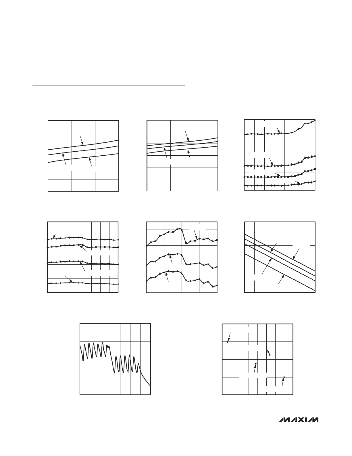
Typical Operating Characteristics
(V
CC_
= 2.8V, TA = +25°C, fLO= 2.5GHz, f
REF
= 40MHz, CS = high, RXHP = SCLK = DIN = low, RF BW = 10MHz, Tx output at 50Ω
unbalanced output of balun, using the MAX2839AS Evaluation Kit.)
DUAL Rx SUPPLY CURRENT
vs. SUPPLY VOLTAGE
SUPPLY VOLTAGE (V)
SUPPLY CURRENT (mA)
MAX2839ASWO+T toc02
2.7 3.0 3.3 3.6
80
90
100
110
120
130
140
TA = -40°C
TA = +25°C
TA = +85°C
Rx MAX GAIN
vs. TEMPERATURE AND FREQUENCY
FREQUENCY (GHz)
RX MAX GAIN (dB)
MAX2939ASWO+T toc05
2.3 2.5 2.62.4 2.7
94
96
98
100
102
TA = -40°C
TA = +25°C
TA = +85°C
RX_B TO RX_A ISOLATION
vs. LNA GAIN SETTING
LNA GAIN SETTING (dB)
RECEIVER ISOLATION (dB)
MAX2839ASWO+T toc08
-35 -25 -15 -5-30 -20 -10 0 5
38
40
42
44
46
LNA = MAX GAIN
LNA = MAX - 8dB
LNA = MAX - 16dB
LNA = MAX - 32dB
SINGLE Rx SUPPLY CURRENT
vs. SUPPLY VOLTAGE
90
85
80
75
TA = +85°C
MAX2839ASWO+T toc01
Rx NOISE FIGURE
vs. BASEBAND GAIN SETTING
40
30
20
LNA = MAX - 32dB
LNA = MAX - 16dB
MAX2839ASWO+T toc03
70
SUPPLY CURRENT (mA)
65
60
TA = +25°C
2.7 3.0 3.3 3.6
SUPPLY VOLTAGE (V)
TA = -40°C
Rx GAIN vs. FREQUENCY
110
LNA = MAX GAIN
100
90
GAIN (dB)
80
LNA = MAX - 32dB
70
60
2.30 2.50 2.602.35 2.55 2.652.40 2.45 2.70
FREQUENCY (GHz)
LNA = MAX - 8dB
LNA = MAX - 16dB
Rx OUTPUT V
1.6
MAX2839ASWO+T toc04
vs. GAIN SETTING
1dB
NOISE FIGURE (dB)
LNA = MAX - 8dB
10
LNA = MAX GAIN
0
0 9 18 27 36 45 54 63
BASEBAND VGA GAIN CODE
Rx VOLTAGE GAIN
vs. BASEBAND GAIN SETTING
120
LNA = MAX - 8dB
80
40
VOLTAGE GAIN (dB)
LNA = MAX - 16dB
LNA = MAX - 32dB
0
0 9 18 27 36 45 54 63
BASEBAND VGA CODE
LNA = MAX
MAX2839ASWO+T toc06
1.2
)
RMS
(V
1dB
0.8
OUTPUT V
0.4
0
0 9 18 27 36 45 54 63
BASEBAND VGA CODE
MAX2839ASWO+T toc07
MAX2839AS
2.3GHz to 2.7GHz MIMO Wireless
Broadband RF Transceiver
______________________________________________________________________________________
11
Typical Operating Characteristics (continued)
(V
CC_
= 2.8V, TA = +25°C, fLO= 2.5GHz, f
REF
= 40MHz, CS = high, RXHP = SCLK = DIN = low, RF BW = 10MHz, Tx output at 50Ω
unbalanced output of balun, using the MAX2839AS Evaluation Kit.)
Rx EVM vs. P
IN
(CHANNEL BANDWIDTH = 10MHz,
64 QAM FUSC)
PIN (dBm)
EVM (%)
MAX2839ASWO+T toc09
-100 -90 -80 -70 -60 -50 -40 -30 -20 -10 0 10
0
2
4
6
8
10
12
14
16
18
20
22
LNA = MAX
LNA = MAX
- 32dB
LNA = MAX
- 16dB
LNA = MAX
- 8dB
0 26.5
Rx EMISSION SPECTRUM AT LNA INPUT
(LNA = MAX GAIN)
MAX2839ASWO+T toc12
FREQUENCY (GHz)
(dBm)
-40
-45
-50
-55
-60
-65
-70
-75
-80
-85
-90
4/3 x LO
4 x LO
WiMAX EVM vs. OFDM JAMMER
(10MHz CHANNEL BANDWIDTH, 64 QAM FUSC)
P
WANTED
= P
SENSITIVITY
+ 3dB = -70.3dBm AT ANTENNA
(INCLUDING 4dB FRONT-END LOSS),
EVM AT P
14
f
12
SENSITIVITY
OFFSET
= 6.37%, WITHOUT JAMMER
=10MHz
Rx EVM vs. V
OUT
(CHANNEL BANDWIDTH = 10MHz,
64 QAM FUSC)
12
LNA = MAX
= -50dBm
P
IN
8
EVM (%)
4
0
-30 -26 -22 -18 -14 -10 -6
V
(dBV
RMS
)
OUT
MAX2839ASWO+T toc10
10
8
EVM (%)
6
4
f
= 20MHz
2
0
-70 -60 -50 -40 -30 -20
P
JAMMER
OFFSET
AT ANTENNA (dBm)
MAX2839ASWO+T toc11
MAX2839AS
2.3GHz to 2.7GHz MIMO Wireless
Broadband RF Transceiver
12 ______________________________________________________________________________________
Typical Operating Characteristics (continued)
(V
CC_
= 2.8V, TA = +25°C, fLO= 2.5GHz, f
REF
= 40MHz, CS = high, RXHP = SCLK = DIN = low, RF BW = 10MHz, Tx output at 50Ω
unbalanced output of balun, using the MAX2839AS Evaluation Kit.)
RXINA± DIFFERENTIAL IMPEDANCE
55.8
55.6
55.4
55.2
55.0
REAL COMPONENT (Ω)
54.8
54.6
54.4
2.30 2.502.40 2.602.35 2.552.45 2.65 2.70
Rx INPUT RETURN LOSS vs. FREQUENCY
0
LNA = MAX GAIN
-5
-10
-15
-20
-25
Rx INPUT RETURN LOSS (dB)
-30
LNA = MAX - 16dB
-35
2300 2400 2500 26002350 2450 2550 2650 2700
vs. FREQUENCY
IMAGINARY
FREQUENCY (GHz)
LNA = MAX - 32dB
LNA = MAX - 8dB
FREQUENCY (MHz)
MAX2839ASWO+T toc13
REAL
-100
-105
-110
-115
-120
IMAGINARY COMPONENT (Ω)
-125
-130
MAX2839ASWO+T toc15
RXINB± DIFFERENTIAL IMPEDANCE
53.6
vs. FREQUENCY
53.4
53.2
53.0
52.8
52.6
REAL COMPONENT (Ω)
52.4
52.2
52.0
2.30 2.652.552.452.35 2.70
IMAGINARY
FREQUENCY (GHz)
MAX2839ASWO+T toc14
REAL
2.602.502.40
RSSI VOLTAGE vs. INPUT POWER
2.5
LNA = MAX
2.0
LNA = MAX - 8dB
1.5
1.0
RSSI VOLTAGE (V)
0.5
0
-110 -80 -50 -20 10
LNA = MAX - 16dB
LNA = MAX - 32dB
PIN (dBm)
-100
-105
-110
-115
-120
IMAGIANRY COMPONENT (Ω)
-125
-130
MAX2839ASWO+T toc16
Rx RSSI STEP RESPONSE
(-32dB SIGNAL STEP)
LNA GAIN
CONTROL
RSSI
200ns/div
MAX2839ASWO+T toc18
3V
0V
1.45V
0.45V
Rx RSSI STEP RESPONSE
(+32dB SIGNAL STEP)
LNA GAIN CONTROL
200ns/div
MAX2839ASWO+T toc17
3V
0V
1.45V
RSSI OUTPUT
0.45V

MAX2839AS
2.3GHz to 2.7GHz MIMO Wireless
Broadband RF Transceiver
______________________________________________________________________________________
13
Typical Operating Characteristics (continued)
(V
CC_
= 2.8V, TA = +25°C, fLO= 2.5GHz, f
REF
= 40MHz, CS = high, RXHP = SCLK = DIN = low, RF BW = 10MHz, Tx output at 50Ω
unbalanced output of balun, using the MAX2839AS Evaluation Kit.)
Rx LPF GROUP DELAY
vs. FREQUENCY
350
300
250
200
150
100
LPF GROUP DELAY (ns)
50
0
0246810121416
CHANNEL BW = 5MHz
CHANNEL BW = 8MHz
CHANNEL BW = 9MHz
CHANNEL BW = 10MHz
FREQUENCY (MHz)
Rx DC OFFSET SETTLING RESPONSE
2V/div
(-16dB BB VGA GAIN STEP)
0V
0V
VGA GAIN
CONTROL
MAX2839ASWO+T toc22
Rx DC OFFSET SETTLING RESPONSE
(+8dB BB VGA GAIN STEP)
2V/div
0V
MAX2839ASWO+T toc19
0V
5mV/div
VGA GAIN
CONTROL
Rx DC OFFSET SETTLING RESPONSE
(-32dB BB VGA GAIN STEP)
2V/div
0V
0V
VGA GAIN
CONTROL
10µs/div
MAX2839ASWO+T toc20
MAX2839ASWO+T toc23
2V/div
5mV/div
2V/div
Rx DC OFFSET SETTLING RESPONSE
(-8dB BB VGA GAIN STEP)
0V
0V
VGA GAIN
CONTROL
10µs/div
Rx BB VGA SETTLING RESPONSE
(+8dB BB VGA GAIN STEP)
VGA GAIN CONTROL
MAX2839ASWO+T toc21
MAX2839ASWO+T toc24
5mV/div
2V/div
1V/div
10µs/div
Rx BB VGA SETTLING RESPONSE
(-8dB BB VGA GAIN STEP)
VGA GAIN CONTROL
0V
200ns/div
MAX2839ASWO+T toc25
5mV/div
2V/div
1V/div
10µs/div
Rx BB VGA SETTLING RESPONSE
(-16dB BB VGA GAIN STEP)
VGA GAIN CONTROL
0V
200ns/div
MAX2839ASWO+T toc26
1V/div
2V/div
1V/div
0V
200ns/div
Rx BB VGA SETTLING RESPONSE
(-32dB BB VGA GAIN STEP)
VGA GAIN CONTROL
0V
200ns/div
MAX2839ASWO+T toc27
MAX2839AS
2.3GHz to 2.7GHz MIMO Wireless
Broadband RF Transceiver
14 ______________________________________________________________________________________
)
Typical Operating Characteristics (continued)
(V
CC_
= 2.8V, TA = +25°C, fLO= 2.5GHz, f
REF
= 40MHz, CS = high, RXHP = SCLK = DIN = low, RF BW = 10MHz, Tx output at 50Ω
unbalanced output of balun, using the MAX2839AS Evaluation Kit.)
Rx LNA SETTLING RESPONSE
(MAX TO MAX - 8dB)
2V/div
LNA GAIN CONTROL
0V
1V/div
200ns/div
10
-10
Rx LNA SETTLING RESPONSE
MAX2839ASWO+T toc28
(MAX TO MAX - 32dB)
2V/div
LNA GAIN CONTROL
0V
1V/div
200ns/div
MAX2839ASWO+T toc29
Rx BB FREQUENCY RESPONSE
CHANNEL BW = 28MHz
0
MAX2839ASWO+T toc30
-20
CHANNEL BW
= 1.5MHz
-30
CHANNEL BW
-40
RESPONSE (dB)
-50
= 5MHz
CHANNEL BW
= 10MHz
-60
-70
0.1 1 10 100
FREQUENCY (MHz

MAX2839AS
2.3GHz to 2.7GHz MIMO Wireless
Broadband RF Transceiver
______________________________________________________________________________________
15
Typical Operating Characteristics (continued)
(V
CC_
= 2.8V, TA = +25°C, fLO= 2.5GHz, f
REF
= 40MHz, CS = high, RXHP = SCLK = DIN = low, RF BW = 10MHz, Tx output at 50Ω
unbalanced output of balun, using the MAX2839AS Evaluation Kit.)
Rx BB FREQUENCY RESPONSE
2
1
0
-1
CHANNEL BW
= 1.5MHz
-2
-3
RESPONSE (dB)
CHANNEL BW
= 5MHz
-4
CHANNEL BW
-5
= 10MHz
-6
0.1 1 10 100
FREQUENCY (MHz)
HISTOGRAM: Rx STATIC DC OFFSET
996
MEAN = 0
DEV = 0.23981mV
830
SAMPLE SIZE = 7841
664
498
332
CHANNEL BW
= 28MHz
MAX2839ASWO+T toc31
5V/div
MAX2839ASWO+T toc34
200mV/div
HISTOGRAM: IQ GAIN IMBALANCE
474
395
316
237
158
79
SAMPLE SIZE = 7839
1σ/div
POWER-ON DC OFFSET CANCELLATION
WITH INPUT SIGNAL
ENABLE
0V
MAX2839ASWO+T toc35
MEAN = 0
DEV = 51.8mV
MAX2839ASWO+T toc32
5V/div
0V
10mV/div
HISTOGRAM: Rx PHASE IMBALANCE
774
MEAN = 0
DEV = 0.11878°
645
SAMPLE SIZE = 7841
516
387
258
129
1σ/div
POWER-ON DC OFFSET CANCELLATION
WITHOUT INPUT SIGNAL
ENABLE
MAX2839ASWO+T toc36
I/Q OUTPUT
MAX2839ASWO+T toc33
166
1σ/div
VGA CODE = -36
LNA GAIN = MAX
I/Q OUTPUT
1µs/div
VGA CODE = -36
LNA GAIN = MAX
1µs/div

MAX2839AS
2.3GHz to 2.7GHz MIMO Wireless
Broadband RF Transceiver
16 ______________________________________________________________________________________
Typical Operating Characteristics (continued)
(V
CC_
= 2.8V, TA = +25°C, fLO= 2.5GHz, f
REF
= 40MHz, CS = high, RXHP = SCLK = DIN = low, RF BW = 10MHz, Tx output at 50Ω
unbalanced output of balun, using the MAX2839AS Evaluation Kit.)
Tx SUPPLY CURRENT vs. SUPPLY VOLTAGE
150
146
142
138
SUPPLY CURRENT (mA)
134
130
2.7 3.0 3.3 3.6
TA = +85°C
TA = +25°C
SUPPLY VOLTAGE (V)
Tx OUTPUT POWER vs. FREQUENCY
(Tx GAIN = MAX - 3dB)
4
3
2
1
(dBm)
0
OUT
P
-1
-2
-3
-4
2300 2350 2400 2450 2500 2550 2600 2650 2700
TA = +85°C
FREQUENCY (MHz)
TA = -40°C
TA = +25°C
TA = -40°C
MAX2839ASWO+T toc37
RESPONSE (dB)
MAX2839ASWO+T toc40
(dBm)
OUT
P
Tx BASEBAND FREQUENCY RESPONSE
10
0
-10
CHANNEL BW
-20
= 1.5MHz
-30
CHANNEL BW
= 5MHz
-40
CHANNEL BW
-50
= 10MHz
-60
-70
0.1 1 10 100
FREQUENCY (MHz)
CHANNEL BW
Tx OUTPUT POWER vs. GAIN SETTING
10
0
-10
-20
-30
TA = +85°C
-40
-50
-60
-70
060503010 20 40
TA = -40°C
TA = +25°C
Tx GAIN CODE
= 28MHz
Tx BASEBAND FREQUENCY RESPONSE
2
MAX2839ASWO+T toc38
-1
-2
-3
RESPONSE (dB)
-4
-5
-6
1
0
CHANNEL BW
= 1.5MHz
CHANNEL BW
= 5MHz
CHANNEL BW
= 10MHz
0.1 1 10 100
CHANNEL BW = 28MHz
FREQUENCY (MHz)
Tx OUTPUT SPECTRUM
(10MHz CHANNEL BANDWIDTH, 16 QAM FUSC)
-70dBr
MAX2839ASWO+T toc41
10dB/div
P
= 0dBm
OUT
0dBr
2.495GHz 2.5GHz 2.555GHz
MAX2839ASWO+T toc39
MAX2839ASWO+T toc42
MASK
Tx OUTPUT SPECTRUM
(10MHz CHANNEL BANDWIDTH, 64 QAM FUSC)
-70dBr
P
= 0dBm
OUT
10dB/div
0dBr
2.495GHz 2.5GHz 2.555GHz
MASK
MAX2839ASWO+T toc43
CARRIER LEAKAGE (dBc)
Tx CARRIER LEAKAGE vs. FREQUENCY
-30
-35
-40
-45
TA = +85°C
-50
-55
-60
2300 2350 2400 2450 2500 2550 2600 2650 2700
TX GAIN SET TO MAX - 3dB
TA = -40°C
TA = +25°C
FREQUENCY (MHz)
MAX2839ASWO+T toc44
Tx CARRIER LEAKAGE vs. GAIN SETTING
-20
-25
-30
TA = +85°C
-35
-40
-45
-50
-55
CARRIER LEAKAGE (dBc)
-60
-65
-70
0 9 18 27 36 45 54 63
TA = +25°C
Tx GAIN CODE
TA = -40°C
MAX2839ASWO+T toc45

MAX2839AS
2.3GHz to 2.7GHz MIMO Wireless
Broadband RF Transceiver
______________________________________________________________________________________
17
Typical Operating Characteristics (continued)
(V
CC_
= 2.8V, TA = +25°C, fLO= 2.5GHz, f
REF
= 40MHz, CS = high, RXHP = SCLK = DIN = low, RF BW = 10MHz, Tx output at 50Ω
unbalanced output of balun, using the MAX2839AS Evaluation Kit.)
Tx SIDEBAND LEVEL vs. FREQUENCY
-30
-35
-40
-45
-50
-55
-60
-65
SIDEBAND LEVEL (dBc)
-70
TA = +25°C
-75
-80
2300 2350 2400 2450 2500 2550 2600 2650 2700
TX GAIN SET TO MAX - 3dB
TA = +85°C
TA = -40°C
FREQUENCY (MHz)
Tx SIDEBAND LEVEL vs. GAIN SETTING
-30
-40
TA = +85°C
MAX2839ASWO+T toc46
-50
-60
SIDEBAND LEVEL (dBc)
-70
-80
0 9 18 27 36 45 54 63
TA = -40°C
Tx GAIN CODE
TA = +25°C
EVM vs. Tx OUTPUT POWER
(64 QAM FUSC, 10MHz CHANNEL BANDWIDTH)
3.0
2.5
MAX2839ASWO+T toc47
2.0
1.5
EVM (%)
1.0
0.5
0
-50 -40 -30 -20 -10 0
P
(dBm)
OUT
MAX2839ASWO+T toc48
Tx OUTPUT EMISSION SPECTRUM
10
0
-10
-20
-30
-40
(dBm)
-50
-60
-70
-80
-90
4/3 x LO
0
2 x LO
3 x LO
4 x LO
5/3 x LO
FREQUENCY (GHz)
Tx OUTPUT RETURN LOSS
vs. FREQUENCY
4
2
0
-2
-4
-6
-8
-10
OUTPUT RETURN LOSS (dB)
-12
-14
-16
2300 2400 2500 2600 2700
FREQUENCY (MHz)
MAX2839ASWO+T toc49
26.5
MAX2839ASWO+T toc52
372
MEAN = -46.235dBc
DEV = 5.1577dB
310
SAMPLE SIZE = 7841
248
186
124
62
1σ/div
Tx MAX OUTPUT POWER OVER FREQUENCY
HISTOGRAM: Tx LO LEAKAGE
6.00
5.00
4.00
(dBm)
3.00
OUT
P
2.00
1.00
TA = -40°C
64QAM OFDM SIGNAL CONFORMING
TO SPECTRAL EMISSION MASK AND
-35dB EVM AFTER I/Q IMBALANCE
CALIBRATION BY MODEM
TA = +25°C
0
2.30 2.45 2.602.35 2.50 2.702.40 2.55 2.65
TA = +85°C
FREQUENCY (GHz)
504
420
MAX2839ASWO+T toc50
336
252
168
84
2.8
2.7
2.6
MAX2839ASWO+T toc53
2.5
2.4
LO FREQUENCY (GHz)
2.3
2.2
2.1
HISTOGRAM: Tx SIDEBAND SUPPRESSION
MEAN = -47.856dBc
DEV = 2.8827dB
SAMPLE SIZE = 7841
1σ/div
LO FREQUENCY vs.
DIFFERENTIAL TUNE VOLTAGE
-1.5 -1.0 -0.5 0 0.5 1.0 1.5 2.0 2.5
DIFFERENTIAL TUNE VOLTAGE (V)
MAX2839ASWO+T toc51
MAX2839ASWO+T toc54

MAX2839AS
2.3GHz to 2.7GHz MIMO Wireless
Broadband RF Transceiver
18 ______________________________________________________________________________________
µ
µ
Typical Operating Characteristics (continued)
(V
CC_
= 2.8V, TA = +25°C, fLO= 2.5GHz, f
REF
= 40MHz, CS = high, RXHP = SCLK = DIN = low, RF BW = 10MHz, Tx output at 50Ω
unbalanced output of balun, using the MAX2839AS Evaluation Kit.)
PHASE NOISE vs. OFFSET FREQUENCY
-50
-60
-70
-80
-90
-100
-110
-120
PHASE NOISE (dBc/Hz)
-130
-140
-150
0.0001 0.001 0.01
OFFSET FREQUENCY (MHz)
0.1 1 10
CHANNEL-SWITCHING FREQUENCY SETTLING
(2.7GHz TO 2.3GHz,
AUTOMATIC VCO SUB-BAND SELECTION)
100kHz
VCO GAIN vs. DIFFERENTIAL TUNE VOLTAGE
80
MAX2839ASWO+T toc55
60
40
VCO GAIN (MHz/V)
20
0
-1.5 -1.0 -0.5 0 0.5 1.0 1.5 2.0 2.5
DIFFERENTIAL TUNE VOLTAGE (V)
CHANNEL-SWITCHING FREQUENCY SETTLING
(2.3GHz TO 2.7GHz,
MANUAL VCO SUB-BAND SELECTION)
100kHz
CHANNEL-SWITCHING FREQUENCY SETTLING
(2.3GHz TO 2.7GHz,
AUTOMATIC VCO SUB-BAND SELECTION)
100kHz
MAX2839ASWO+T toc56
20kHz/div
-100kHz
0
TIME (ms)
CHANNEL-SWITCHING FREQUENCY SETTLING
(2.7GHz TO 2.3GHz,
MANUAL VCO SUB-BAND SELECTION)
100kHz
MAX2839ASWO+T toc57
1.498
20kHz/div
-100kHz
MAX2839ASWO+T toc58
20kHz/div
100kHz
0
TIME (ms)
1.498
0
TIME (µs)
Tx-TO-Rx TURNAROUND FREQUENCY
GLITCH SETTLING
2V/div
10kHz/div
FREQUENCY ERROR
1
MAX2839ASWO+T toc61
Tx TO Rx SWITCHING
10kHz/div
s/div
MAX2839ASWO+T toc59
20kHz/div
-100kHz
199.89
0
Rx-TO-Tx TURNAROUND FREQUENCY
GLITCHING SETTLING
2V/div
FREQUENCY ERROR
1µs/div
TIME (
MAX2839ASWO+T toc62
Rx TO Tx SWITCHING
s)
MAX2839ASWO+T toc60
199.89

MAX2839AS
2.3GHz to 2.7GHz MIMO Wireless
BroadbandRF Transceiver
______________________________________________________________________________________ 19
Bump Description
BUMP NAME FUNCTION
1 GNDRXLNA_A Receiver A LNA Ground
2V
3V
4 GND_LNA_B Receiver B LNA Ground
5 RXINB+ Receiver B LNA Differential Input Plus. Input is internally DC-coupled.
6 GND_MXR_B Receiver B Mixer Ground
7 B2 Receiver and Transmitter Gain-Control Logic Input Bit 2
8 B3 Receiver and Transmitter Gain-Control Logic Input Bit 3
9 B4 Receiver and Transmitter Gain-Control Logic Input Bit 4
10 V
11 GND1_PAD_RF Transmit Power Amplifier Driver Ground
12 GND2_PAD_RF Transmit Power Amplifier Driver Ground
13 PABIAS Transmit External Power Amplifier Bias DAC Output
14 GND_TXMX Transmit Upconverter Ground
15 SCLK Serial-Clock Logic Input of 4-Wire Serial Interface
16 REFCLK Reference Clock Input. AC-couple a reference clock to this analog input.
17 V
18 V
19 GNDCP Charge-Pump Ground
20 CPOUT+
21 GNDVCO VCO Ground
22 VCOBYP
23 V
24 GND_LO Local Oscillator Generation Ground
25 CS Active-Low Chip-Select Logic Input of 4-Wire Serial Interface
26 GND_RXBB_B Receiver B Baseband Ground
27 RXBBIB+ Receiver B Baseband I-Channel Differential Output Plus
28 RXBBQB+ Receiver B Baseband Q-Channel Differential Output Plus
29 B6 Receiver and Transmitter Gain-Control Logic Input Bit 6
30 RXBBQA- Receiver A Baseband Q-Channel Differential Output Minus
31 RXBBQA+ Receiver A Baseband Q-Channel Differential Output Plus
32 V
33 GND_RXBB_A Receiver A Baseband Ground
34 GND_RXLOGEN Receiver Divide-by-2 Ground
35 GND_MXR_A Receiver A Mixer Ground
36 GND_LNA_A Receiver A LNA Ground
37 TXBBQ- Transmitter Baseband Q-Channel Differential Input Minus
38 CLKOUT_DIV Clockout Divide Ratio Select Logic Input
CCRXLNA_A
CCRXLNA_B
CCTXPAD
CCXTAL
CCCP
CCVCO
CCRXVGA
Receiver A LNA Supply Voltage. Bypass with a 22pF capacitor as close as possible to the pin.
Receiver B LNA Supply Voltage. Bypass with a 22pF capacitor as close as possible to the pin.
Supply Voltage for Transmitter Power Amplifier Driver. Bypass with a 22pF capacitor as close as
possible to the pin.
Crystal Oscillator Supply Voltage. Bypass with a 100nF capacitor as close as possible to the pin.
PLL Charge-Pump Supply Voltage. Bypass with a 100nF capacitor as close as possible to the pin.
Differential Charge-Pump Output Plus. Connect the frequency synthesizer’s loop filter between
CPOUT+ and CPOUT- (see the Typical Operating Circuit).
On-Chip VCO Regulator Output Bypass. Bypass with a 1µF capacitor to GND. Do not connect other
circuitry to this point.
VCO Supply Voltage. Bypass with a 22nF capacitor as close as possible to the pin.
Receiver VGA Supply Voltage. Bypass with a 100nF capacitor as close as possible to the pin.

MAX2839AS
2.3GHz to 2.7GHz MIMO Wireless
Broadband RF Transceiver
20 ______________________________________________________________________________________
Bump Description (continued)
BUMP NAME FUNCTION
39 GNDRXLNA_B Receiver B LNA Ground
40 RXINB- Receiver B LNA Differential Input Minus. Input is internally DC-coupled.
41 TXRX Transmit/Receive Mode Enable Logic Input
42 B5 Receiver and Transmitter Gain-Control Logic Input Bit 5
43 TXOUT+ Power Amplifier Driver Differential Output Plus. The pin is biased at VCC/2 internally.
44 B1 Receiver and Transmitter Gain-Control Logic Input Bit 1
45 TXOUT- Power Amplifier Driver Differential Output Minus. The pin is biased at VCC/2 internally.
46 V
47 CLKOUT Reference Clock Buffer Output
48 GND_XTAL Crystal Oscillator Ground
49 GND_DIG PLL Digital Ground
50 V
51 CPOUT-
52, 67 GND Ground. Connect to the PCB ground plane.
53 DIN Data Logic Input of 4-Wire Serial Interface
54 GND_PAD_BIAS Transmit Bias Ground
55 XTAL1 XTAL Input. AC-couple crystal to this analog pin.
56 RXHP Receiver I- and Q-Channel AC-Coupling Highpass Corner Frequency Selection Logic Input
57 RXBBIA- Receiver A Baseband I-Channel Differential Output Minus
58 RXBBIA+ Receiver A Baseband I-Channel Differential Output Plus
59 TXBBI+ Transmitter Baseband I-Channel Differential Input Plus
60 TXBBQ+ Transmitter Baseband Q-Channel Differential Input Plus
61 V
62 RXINA- Receiver A LNA Differential Input Minus. Input is internally DC-coupled.
63 RXINA+ Receiver A LNA Differential Input Plus. Input is internally DC-coupled.
64 B0 Receiver and Transmitter Gain-Control Logic Input Bit 0
65 ENABLE Transceiver Enable Logic Input
66 DOUT Data Logic Output of 4-Wire Serial Interface
68 RXBBIB- Receiver B Baseband I-Channel Differential Output Minus
69 RXBBQB- Receiver B Baseband Q-Channel Differential Output Minus
70 RSSI Receiver Signal Strength Output
71 B7 Receiver Gain-Control Logic Input Bit 7
72 V
73 TXBBI- Transmitter Baseband I-Channel Differential Input Minus
CCTXMX
CC_DIG
CCRXMX
CCRXFL
Transmitter Upconverter Supply Voltage. Bypass with a 22pF capacitor as close as possible to the
pin.
PLL Digital Supply Voltage. Bypass with a 100nF capacitor as close as possible to the pin.
Differential Charge-Pump Output Minus. Connect the frequency synthesizer’s loop filter between
CPOUT+ and CPOUT- (see the Typical Operating Circuit).
Receiver Downconverters Supply Voltage. Bypass with a 22pF capacitor as close as possible to the
pin.
Receiver Baseband Filter Supply Voltage. Bypass with a 100nF capacitor as close as possible to
the pin.

MAX2839AS
2.3GHz to 2.7GHz MIMO Wireless
BroadbandRF Transceiver
______________________________________________________________________________________ 21
Detailed Description
Modes of Operation
The modes of operation for the MAX2839AS are shutdown, clock-out only, standby, receive, transmit, transmitter calibration, and receiver calibration. See Table 1
for a summary of the modes of operation. When the
parts are active, various blocks can be shutdown individually by programming different SPI registers.
Shutdown Mode
The MAX2839AS features a low-power shutdown mode.
In shutdown mode, all circuit blocks are powered down,
except the 4-wire serial bus and its internal programmable registers.
Clock-Out Only
In clock-out mode, the entire transceiver is off except
the divided reference clock output on the CLKOUT pin
and the clock divider, which remain on.
Standby Mode
The standby mode is used to enable the frequency
synthesizer block while the rest of the device is powered down. In this mode, the PLL, VCO, and LO gener-
ator are on so that Tx or Rx modes can be quickly
enabled from this mode. These and other blocks can
be selectively enabled in this mode by programming
different SPI registers.
Receive (Rx) Mode
In receive mode, all Rx circuit blocks are powered on
and active. Antenna signal is applied; RF is downconverted, filtered, and buffered at Rx BB I and Q outputs.
Either receiver A or both receivers can be enabled.
Receiver B cannot be enabled by itself.
Transmit (Tx) Mode
In transmit mode, all Tx circuit blocks are powered on.
The external PA is powered on after a programmable
delay using the on-chip PA bias DAC.
Transmitter (Tx) Calibration Mode
All Tx circuit blocks except PA driver and external PA
are powered on and active. The AM detector and
receiver I/Q channel buffers are also on, along with
multiplexers in the receiver side to route this AM detector’s signal to each I and Q differential outputs. When
required, the I/Q lowpass filter can be bypassed.
Table 1. Operating Mode
MODE CONTROL LOGIC INPUTS CIRCUIT BLOCK STATES
MODE
Shutdown 0 0 X XX Off Off Off None Off
Clock-Out Only 1 X X X0 Off Off Off None On
Clock-Out Only X 1 X X0 Off Off Off None On
Standby 0 1 X 01 Off Off On or Off None On
Rx (1x2 MIMO) 1 1 1 01 On Off On None On
Rx (1x1 SISO) 1 1 0 01 On (RX_A) Off On None On
Tx 1 0 X 01 Off On On None On
Tx Calibration 1 0 X 11 Off
RX_A
Calibration
(Loopback)
RX_B
Calibration
(Loopback)
ENABLE
PIN
TXRX
PIN
11011
11111
SPI
REG1
D<3>
SPI
REG16
D<1:0>
Rx PATH Tx PATH
On (except
PA driver)OnSPI REG7D<7> = 1
On
(except
LNA)
On
(except
LNA)
On (except
PA driver)OnS P I RE G26D < 3> = 1
On (except
PA driver)OnS P I RE G26D < 3> = 1
PLL, VCO, LO
GEN
CALIBRATION
SECTIONS ON
AM detector + Rx
I, Q buffers
Loopback On
Loopback On
CLOCK
O U T PU T
On

MAX2839AS
2.3GHz to 2.7GHz MIMO Wireless
Broadband RF Transceiver
22 ______________________________________________________________________________________
Receiver (Rx) Calibration or Loopback
Part of the Rx and Tx circuit blocks except LNA and PA
driver are powered on and active. The transmitter I/Q
input signals are upconverted to RF, and the output of
the Tx gain control block (VGA) is fed to the receiver at
the input of the downconverter. Either receiver A or
both receivers can be connected to the transmitter and
powered on. The I/Q lowpass filters are not present in
the transmitter signal path (they are bypassed).
Programmable Registers
and 4-Wire SPI Interface
The MAX2839AS includes 32 programmable 16-bit registers. The most significant bit (MSB) is the read/write
selection bit. The next 5 bits are register address. The
10 least significant bits (LSBs) are register data.
Register data is loaded through the 4-wire
SPI/MICROWIRE™-compatible serial interface. Data at
DIN is shifted in MSB first and is framed by CS. When
CS is low, the clock is active, and input data is shifted
at the rising edge of the clock. During the read mode,
register data selected by address bits is shifted out to
DOUT at the falling edges of the clock. At the CS rising
edge, the 10-bit data bits are latched into the register
selected by address bits. See Figure 1. The register
values are preserved in shutdown mode as long as the
power-supply voltage is maintained. After power-up,
the user must program all register values.
Figure 1. 4-Wire SPI Serial-Interface Timing Diagram
MICROWIRE is a trademark of National Semiconductor Corp.
DOUT
DIN
SCLK
BIT 1
BIT 2
DON'T CARE
BIT 6
BIT 14 BIT 13 BIT 5
t
CH
t
CS
DOUT
DIN
SCLK
CS
t
t
CSS
CSO
BIT 1
DS
BIT 2
t
DH
DON'T CARE
SPI REGISTER WRITE
BIT 5
SPI REGISTER READ
t
CL
t
BIT 6
t
D
BIT 13
DON'T CARE
CSH
t
CSW
BIT 14
t
CS1

MAX2839AS
2.3GHz to 2.7GHz MIMO Wireless
BroadbandRF Transceiver
______________________________________________________________________________________ 23
SPI Register Definitions
(All values in the register definition table are typical numbers. The MAX2839AS SPI does not have a power-on-default feature; the
user must program all SPI addresses for normal operation. Prior to use of any untested settings, contact the factory.)
Table 2. MAX2839AS Register Summary
REGISTER NO.
FUNCTIONS
0 RX_ENABLE 000 Reserved for internal use
1 RX_RF_1 00C
• LNA band select, MIMO mode select
• Rx I/Q phase error correction
2 RX_RF_2 081
• LNA gain SPI control enable
• Rx I/Q phase error SPI control enable
3 RX_RF/LPF 1B9 Reserved for internal use
4 LPF 3E6 • RF channel bandwidth select
5 LPF/VGA_1 100
• RX_A LNA and VGA gain controls
• LPF operating mode select
6 LPF/VGA_2 000
• RX_B LNA and VGA gain controls
• Rx VGA common-mode select
7 RSSI/VGA 208
• RSSI pin output select, operating mode as a function of RXHP, and receiver
select
• Rx baseband outputs routing select
8 RX_TOP_SPI_1 222
• Rx VGA gain SPI control enable
• LPF operating mode select enable
9 RX_TOP_SPI_2 018
• Temperature sensor enable, and ADC readout trigger
• DOUT output selection, drive select, three-state output select
10 TX_TOP_ SPI 00C • Tx AM detector gain and filter bandwidth controls
11 TEMP_SEN 004 • Temperature sensor ADC readout
12 HPFSM 1 24F
• 10MHz HPC duration select when triggered by RXEN or LNA gain
• 600kHz HPC duration select when triggered by RXEN or LNA gain
13 HPFSM 2 150
• 100kHz HPC duration select when triggered by RXEN or LNA gain
• 30kHz HPC duration select when triggered by RXEN or LNA gain
• 1kHz HPC duration select when triggered by RXEN
14 HPFSM 3 3C5
• 1kHz HPC duration select when triggered by LNA gain
• HPC rising edge delay and final highpass corner select
• HPC on-hold corner select as a function of RXHP
• HPC state machine retriggered by LNA gain enable
15 HPFSM 4 201
• HPC state machine clock divider, sequence bypass, and RXHP dependent
select
16 BLK_SPI_EN 01C • Block enabled by SPI
17 FRAC_DIV_1 155 • Last 10 of 20 fractional divider bits
18 FRAC_DIV_2 155 • First 10 of 20 fractional divider bits
19 INT_DIV 153
• Integer divider bits
• LO generation band select
20
249
• Reference divider ratio
• CLKOUT buffer drive select
21
02D Reserved for internal use
REGISTER NAME DEFAULT
SYNTH_CONFIG_1
SYNTH_CONFIG_2

MAX2839AS
2.3GHz to 2.7GHz MIMO Wireless
Broadband RF Transceiver
24 ______________________________________________________________________________________
Table 2. MAX2839AS Register Summary (continued)
REGISTER NO.
FUNCTIONS
22 VAS_CONFIG 1A9
• VAS operating mode select, relock location, clock divide ratio, delay counter
ratio, and triggering
23
24F
• VAS sub-band SPI overwrite
• Crystal oscillator bias select
24 XTAL_CONFIG 180 • Crystal oscillator core enable, and frequency tuning
25 VCO_CONFIG 000 Reserved for internal use
26
3C0
• VAS test signal select
• VTUNE test signal select
• LOGEN G
m
enable
27
280
• Tx LO I/Q phase adjustment by SPI enable, and phase adjustment select
• Tx DC correction by SPI enable
• Tx VGA gain control by SPI enable
28 PA_BIAS_ DAC 0C0 • PA DAC output current select, and turn-on delay control
29
03F • Tx VGA gain control
30
380
• Tx DC offset correction for I-channel
• PA DAC output type select, and voltage mode output select
31
340
• Tx DC offset correction for Q-channel
• PA DAC clock-divide ratio
ADDRESS BITS DATA BITS
REGISTER NAME
D0
RX_ENABLE 0 0 0 000000000000
RX_RF_1 0 0 0 010000001100
RX_RF_2 0 0 0 100010000001
RX_RF/LPF 0 0 0 110110111001
LPF 001001111100110
LPF/VGA_1 0 0 1 010100000000
LPF/VGA_2 0 0 1 100000000000
RSSI/VGA 0 0 1 111000001000
RX_TOP_SPI_1 0 1 0 001000100010
RX_TOP_SPI_2 0 1 0 010000011000
TX_TOP_ SPI 0 1 0 100000001100
TEMP_SEN 0 1 0 110000000100
HPFSM 1 0 1 1 001001001111
HPFSM 2 0 1 1 010101010000
HPFSM 3 0 1 1 101111000101
HPFSM 4 0 1 1 111000000001
BLK_SPI_EN 1 0 0 000000011100
FRAC_DIV_1 1 0 0 010101010101
FRAC_DIV_2 1 0 0 100101010101
INT_DIV 1 0 0 110101010011
REGISTER NAME DEFAULT
LO_MISC_CONFIG
LOGEN_CONFIG
TXLO_I/Q_CONFIG
TX_GAIN_CONFIG
TX_DC CORR_1
TX_DC_CORR_2
A4 A3 A2 A1 A0 D9 D8 D7 D6 D5 D4 D3 D2 D1

MAX2839AS
2.3GHz to 2.7GHz MIMO Wireless
BroadbandRF Transceiver
______________________________________________________________________________________ 25
Table 2. MAX2839AS Register Summary (continued)
ADDRESS BITS DATA BITS
REGISTER NAME
D0
SYNTH_CONFIG_1 1 0 1 001001001001
SYNTH_CONFIG_2 1 0 1 010000101101
VAS_CONFIG 1 0 1 100110101001
LO_MISC_CONFIG 1 0 1 111001001111
XTAL_CONFIG 1 1 0 000110000000
VCO_CONFIG 1 1 0 010000000000
LOGEN_CONFIG 1 1 0 101111000000
TXLO_I/Q_CONFIG 1 1 0 111010000000
PA_BIAS_ DAC 1 1 1 000011000000
TX_GAIN_CONFIG 1 1 1 010000111111
TX_DC CORR_1 1 1 1 101110000000
TX_DC_CORR_2 1 1 1 111101000000
Table 3. Register 0: RX_ENABLE Register (Address = 00000, Default = 000
HEX
)
BIT NAME
(0 = LSB)
DESCRIPTION
RESERVED 9:0 Reserved bits—set to default
Table 4. Register 1: RX_RF_1 Register (Address = 00001, Default = 00C
HEX
)
BIT NAME
(0 = LSB)
DESCRIPTION
RESERVED 9:4 Reserved bits—set to default
MIMO_MODE_SEL 3
MIMO mode selection.
0 = RX_A
1 = RX_A + RX_B (default)
RESERVED 2:1 Reserved bits—set to default
LNA_BAND 0
LNA output LC tank center frequency select.
0 = 2.3GHz to 2.5GHz (default)
1 = 2.5GHz to 2.7GHz
Table 5. Register 2: RX_RF_2 Register (Address = 00010, Default = 081
HEX
)
BIT NAME
(0 = LSB)
DESCRIPTION
RESERVED 9:1 Reserved bits—set to default
LNA_GAIN_SPI_EN 0
LNA gain control select.
0 = LNA gain controlled by external pins B7 and B6
1 = LNA gain controlled by SPI through register 6 bits 1:0 (default)
A4 A3 A2 A1 A0 D9 D8 D7 D6 D5 D4 D3 D2 D1
BIT LOCATION
BIT LOCATION
BIT LOCATION

MAX2839AS
2.3GHz to 2.7GHz MIMO Wireless
Broadband RF Transceiver
26 ______________________________________________________________________________________
Table 6. Register 3: RX_RF/LPF Register (Address = 00011, Default = 1B9
HEX
)
BIT NAME
(0 = LSB)
DESCRIPTION
RESERVED 9:0 Reserved bits—set to default
Table 7. Register 4: LPF Register (Address = 00100, Default = 3E6
HEX
)
BIT NAME
(0 = LSB)
DESCRIPTION
FT<3:0> 9:6
RF channel bandwidth select.
Test at RFBW 5MHz, 10MHz, and 28MHz.
0000 = 1.75MHz
0001 = 2.5MHz
0010 = 3.5MHz
0011 = 5.0MHz
0100 = 5.5MHz
0101 = 6.0MHz
0110 = 7.0MHz
0111 = 8.0MHz
1000 = 9.0MHz
1001 = 10.0MHz
1010 = 12.0MHz
1011 = 14.0MHz
1100 = 15.0MHz
1101 = 20.0MHz
1110 = 24.0MHz
1111 = 28.0MHz (default)
RESERVED 5:0 Reserved bits—set to default
Table 8. Register 5: LPF/VGA_1 Register (Address = 00101, Default = 100
HEX
)
BIT NAME
(0 = LSB)
DESCRIPTION
RESERVED 9:8 Reserved bits—set to default
VGA1<5:0> 7:2
Receiver 1 VGA attenuation settings through SPI.
Active when register 8 D<1> = 1.
000000 = Max gain (default)
000001 = Max - 1dB
……….
111110 = Max - 62dB
111111 = Max - 63dB (min gain)
Test at settings 000000, 000001, 001000, 010000, 100000, 110110, and
111111.
LNA1<1:0> 1:0
Receiver 1 LNA gain settings through SPI.
Active when register 2 D<0> = 1.
00 = Max gain (default)
01 = Max - 8dB
10 = Max - 16dB
11 = Max - 32dB
BIT LOCATION
BIT LOCATION
BIT LOCATION

MAX2839AS
2.3GHz to 2.7GHz MIMO Wireless
BroadbandRF Transceiver
______________________________________________________________________________________ 27
Table 9. Register 6: LPF/VGA_2 Register (Address = 00110, Default = 000
HEX
)
BIT NAME
(0 = LSB)
DESCRIPTION
BUFF_VCM<1:0> 9:8
Rx VGA output common-mode voltage select.
00 = 1.05V (default)
01 = 1.15V
10 = 1.25V
11 = 1.45V
VGA2<5:0> 7:2
Receiver 2 VGA attenuation settings through SPI.
Active when register 8 D<1> = 1.
000000 = Max gain (default)
000001 = Max - 1dB
……….
111110 = Max - 62dB
111111 = Max - 63dB (min gain)
Test at settings 000000, 000001, 001000, 010000, 100000, 110110, and
111111.
LNA2<1:0> 1:0
Receiver 2 LNA gain settings through SPI.
Active when register 2 D<0> = 1.
00 = Max gain (default)
01 = Max - 8dB
10 = Max - 16dB
11 = Max - 32dB
Table 10. Register 7: RSSI/VGA Register (Address = 00111, Default = 208
HEX
)
BIT NAME
(0 = LSB)
DESCRIPTION
RSSI_RXSEL 9
RSSI for receiver 1 or 2 select.
0 = RSSI for receiver 2
1 = RSSI for receiver 1 (default)
RESERVED 8 Reserved bits—set to default
SEL_IN1_IN2 7
RXBBI output select.
0 = Select Rx VGA output (default)
1 = Select Tx AM detector output
RESERVED 6:0 Reserved bits—set to default
BIT LOCATION
BIT LOCATION

MAX2839AS
2.3GHz to 2.7GHz MIMO Wireless
Broadband RF Transceiver
28 ______________________________________________________________________________________
Table 11. Register 8: RX_TOP_SPI_1 Register (Address = 01000, Default = 222
HEX
)
BIT NAME
(0 = LSB)
DESCRIPTION
RESERVED 9:3 Reserved bits—set to default
LPF_MODE_SEL 2
LPF operating mode select.
0 = LPF response changes automatically between Tx and Rx by TXRX pin
(default)
1 = LPF response fixed in Tx, Rx, calibration, or trim mode as defined in
register 5 D<9:8>
VGA_GAIN _SPI_EN 1
Rx VGA gain control through SPI.
0 = Rx VGA gain controlled by external pins B5:B1
1 = Rx VGA gain controlled by SPI (default)
RESERVED 0 Reserved bits—set to default
Table 13. Register 10: TX_TOP_SPI Register (Address = 01010, Default = 00C
HEX
)
BIT NAME
(0 = LSB)
DESCRIPTION
RESERVED 9:2 Reserved bits—set to default
TXCAL_GAIN<1:0> 1:0
Transmit AM detector baseband gain control select.
00 = Minimum gain (default)
01 = +10dB
10 = +20dB
11 = +30dB
Table 12. Register 9: RX_TOP_SPI_2 Register (Address = 01001, Default = 018
HEX
)
BIT NAME
(0 = LSB)
DESCRIPTION
RESERVED 9:8 Reserved bits—set to default
DOUT_SEL<2:0> 7:5
DOUT pin multiplexed output select.
000 = SPI register (default)
001 = PLL lock detect. Set register 21 D<9:7> = 000 for lock-detect out.
010 = VAS and VTUNE outputs defined by register 26 D<9:6>
DOUT_CSB_SEL 4
DOUT pin three-state control.
0 = DOUT pin is independent of CSB pin
1 = DOUT pin is in three-state mode when CSB is high (default)
DOUT_DRVH 3
DOUT pin output drive select.
0 = 1x drive. Delay < 4.4ns.
1 = 4x drive. Delay < 3.1ns (default).
RESERVED 2 Reserved bits—set to default
TS_EN 1
Temperature sensor comparator and clock enable.
0 = Disabled (default)
1 = Enabled
TS_ADC_TRIG 0
Temperature sensor ADC trigger.
0 = Not trigger ADC readout (default)
1 = Trigger ADC readout. ADC is disabled automatically after readout
finishes.
BIT LOCATION
BIT LOCATION
BIT LOCATION

MAX2839AS
2.3GHz to 2.7GHz MIMO Wireless
BroadbandRF Transceiver
______________________________________________________________________________________ 29
Table 14. Register 11: TEMP_SEN Register (Address = 01011, Default = 004
HEX
)
BIT NAME
(0 = LSB)
DESCRIPTION
RESERVED 9:0
Reserved bits—set to default.
Readout at DOUT pin through SPI A[4:0] = 01011, D[4:0]
Table 15. Register 12: HPFSM 1 Register (Address = 01100, Default = 24F
HEX
)
BIT NAME
(0 = LSB)
DESCRIPTION
HPC_600k_GAIN<2:0> 9:7
Rx VGA highpass corner duration at 600kHz. Triggered by LNA gain
change. Test at settings 000, 001, and 011.
000 = 0µs
001 = 0.8µs
010 = 1.6µs
011 = 2.4µs
100 = 3.2µs (default)
101 = 4.0µs
110 = 4.8µs
111 = stay “1”
HPC_600k<2:0> 6:4
Rx VGA highpass corner duration at 600kHz. Triggered by RXEN rising
edge. Test at settings 000, 100, and 110.
000 = 0µs
001 = 0.8µs
010 = 1.6µs
011 = 2.4µs
100 = 3.2µs (default)
101 = 4.0µs
110 = 4.8µs
111 = stay “1”
HPC_10M_GAIN<1:0> 3:2
Rx VGA highpass corner duration at 10MHz. Triggered by LNA gain
change. Test at settings 00, 01, and 11.
00 = 0µs
01 = 0.4µs
10 = 0.8µs
11 = 1.2µs (default)
HPC_10M<1:0> 1:0
Rx VGA highpass corner duration 10MHz. Triggered by RXEN rising edge.
Test at settings 00 and 11.
00 = 0µs
01 = 0.4µs
10 = 0.8µs
11 = 1.2µs (default)
BIT LOCATION
BIT LOCATION

MAX2839AS
2.3GHz to 2.7GHz MIMO Wireless
Broadband RF Transceiver
30 ______________________________________________________________________________________
Table 16. Register 13: HPFSM 2 Register (Address = 01101, Default = 150
HEX
)
BIT NAME
(0 = LSB)
DESCRIPTION
HPC_1k<1:0> 9:8
Rx VGA highpass corner duration at 1kHz. Triggered by RXEN rising edge.
Test at settings 00, 01, and 11.
00 = 0µs
01 = 3.2µs (default)
10 = 6.4µs
11 = 9.6µs
HPC_30k_GAIN<1:0> 7:6
Rx VGA highpass corner duration at 30kHz. Triggered by LNA gain change.
Test at settings 00 and 01.
00 = 0µs
01 = 3.2µs (default)
10 = 6.4µs
11 = 9.6µs
HPC_30k<1:0> 5:4
Rx VGA highpass corner duration at 30kHz. Triggered by RXEN rising edge.
Test at settings 00, 01, and 10.
00 = 0µs
01 = 3.2µs (default)
10 = 6.4µs
11 = 9.6µs
HPC_100k_GAIN<1:0> 3:2
Rx VGA highpass corner duration at 100kHz. Triggered by LNA gain
change. Test at settings 00 and 11.
00 = 0µs (default)
01 = 3.2µs
10 = 6.4µs
11 = 9.6µs
HPC_100k<1:0> 1:0
Rx VGA highpass corner duration at 100kHz. Triggered by RXEN rising
edge. Test at settings 00, 01, and 11.
00 = 0µs (default)
01 = 3.2µs
10 = 6.4µs
11 = 9.6µs
BIT LOCATION

MAX2839AS
2.3GHz to 2.7GHz MIMO Wireless
BroadbandRF Transceiver
______________________________________________________________________________________ 31
Table 17. Register 14: HPFSM 3 Register (Address = 01110, Default = 3C5
HEX
)
BIT NAME
(0 = LSB)
DESCRIPTION
TXGATE_EN 9
PA driver and DAC on/off state gated by PLL lock detect.
0 = Independent of PLL lock detect
1 = Disable PA driver when PLL lock detect = 0 (default)
RESERVED 8 Reserved bits—set to default
HPC_STOP_M2<1:0> 7:6
Rx VGA on-hold highpass corner when RXHP = 1. Test at settings 00, 01, and
11. Only active when Reg15_D9 = 1.
00 = 1kHz
01 = 30kHz
10 = 100kHz
11 = 600kHz (default)
HPC_STOP<1:0> 5:4
Rx VGA final highpass corner selection. Test at settings 00, 01, and 11.
00 = 100Hz (default)
01 = 1kHz
10 = 30kHz
11 = 100kHz
HPC_DELAY<1:0> 3:2
Rx VGA HPC
A
and HPCD rising edge delay for 100k, 30k, 1k, and 100Hz
highpass corner. Test at settings 00, 01, and 11.
00 = 0µs
01 = 0.2µs (default)
10 = 0.4µs
11 = 0.6µs
HPC_1k_GAIN<1:0> 1:0
Rx VGA highpass corner duration at 1kHz. Triggered by LNA gain change.
Test at settings 00, 01, and 10.
00 = 0µs
01 = 3.2µs (default)
10 = 6.4µs
11 = 9.6µs
Table 18. Register 15: HPFSM 4 Register (Address = 01111, Default = 201
HEX
)
BIT NAME
(0 = LSB)
DESCRIPTION
HP_MODE 9
Highpass corner control using RXHP.
0 = Highpass corner switches automatically without RXHP
1 = Highpass corner switches dependent on RXHP (default)
RESERVED 8:7 Reserved bits—set to default
HPC_SEQ_BYP 6
Highpass corner switching sequence bypassed during RXHP transition from
1 to 0.
0 = Start switching from highpass corner set by HPC_STOP_M2<1:0> in
register 14 and continue with programmed sequence (default)
1 = Switch from highpass corner set by HPC_STOP_M2<1:0> directly to
final highpass corner set by HPC_STOP<1:0> in register 14.
RESERVED 5:0 Reserved bits—set to default
BIT LOCATION
BIT LOCATION

MAX2839AS
2.3GHz to 2.7GHz MIMO Wireless
Broadband RF Transceiver
32 ______________________________________________________________________________________
Table 19. Register 16: BLK_SPI_EN Register (Address = 10000, Default = 01C
HEX
)
BIT NAME
(0 = LSB)
DESCRIPTION
RESERVED 9:8 Reserved bits—set to default
PADAC_TX_EN 7
PA bias DAC Tx mode enable bit. Enables PA bias DAC only in Tx mode.
Turn-on delay is controlled by bits 9:6 of register 28.
0 = Disabled (default)
1 = Enabled when TXRX = 0
PADAC_SPI_EN 6
PA bias DAC SPI enable bit. Turn-on delay is controlled by bits 9:6 of
register 28.
0 = Disabled (default)
1 = Enabled in all modes except for shutdown
RESERVED 5:2 Reserved bits—set to default
CAL_SPI 1
Receive and transmit calibration mode enable bit. Rx or Tx calibration mode
is selected by TXRX pin.
0 = Normal receive or transmit mode (default)
1 = Calibration mode
EN_SPI 0
Transceiver enable bit.
0 = Disabled (default)
1 = Enabled. Enable pin must also be 1 to turn on transceiver.
Table 20. Register 17: FRAC_DIV_1 Register (Address = 10001, Default = 155
HEX
)
BIT NAME
(0 = LSB)
DESCRIPTION
SYN_CONFIG0<9:0> 9:0
Bits 9:0 of the 20-bit fractional divide ratio. The remaining bits 19:10 reside
in register 18. Both registers are combined to form the 20-bit fractional word.
Program register 17 to engage the stored values of registers 18 and 19.
Table 21. Register 18: FRAC_DIV_2 Register (Address = 10010, Default = 155
HEX
)
BIT NAME
(0 = LSB)
DESCRIPTION
SYN_CONFIG0<19:10> 9:0
Bits 19:10 of the 20-bit fractional divide ratio. The remaining bits 9:0 reside
in register 17. Both registers are combined to form the 20-bit fractional word.
Program register 18 before register 17.
BIT LOCATION
BIT LOCATION
BIT LOCATION

MAX2839AS
2.3GHz to 2.7GHz MIMO Wireless
BroadbandRF Transceiver
______________________________________________________________________________________ 33
Table 22. Register 19: INT_DIV Register (Address = 10011, Default = 153
HEX
)
BIT NAME
(0 = LSB)
DESCRIPTION
LOGEN_BSW<1:0> 9:8
LO generation band switch control for optimal transmit spur.
00 = 2300MHz to 2399.99MHz
01 = 2400MHz to 2499.99MHz (default)
10 = 2500MHz to 2599.99MHz
11 = 2600MHz to 2700MHz
SYN_CONFIG1<7:0> 7:0
Synthesizer 8-bit integer divide ratio.
Program register 19 before register 17. Test at settings between 76 and 90
to support LO frequency between 2300MHz and 2700MHz.
Table 23. Register 20: SYNTH_CONFIG_1 Register (Address = 10100, Default = 249
HEX
)
BIT NAME
(0 = LSB)
DESCRIPTION
RESERVED 9:6 Reserved bits—set to default
CLKOUT_DRV 5
Reference clock output buffer drive selection.
0 = 1x drive (default)
1 = 4x drive
RESERVED 4:3 Reserved bits—set to default
SYN_CONFIG1<1:0> 2:1
Reference divide ratio selection.
00 = Divide by 1 (default)
01 = Divide by 2
10 = Divide by 4
RESERVED 0 Reserved bit—set to default
Table 24. Register 21: SYNTH_CONFIG_2 Register (Address = 10101, Default = 02D
HEX
)
BIT NAME
(0 = LSB)
DESCRIPTION
RESERVED 9:0 Reserved bits—set to default
Table 25. Register 22: VAS_CONFIG Register (Address = 10110, Default = 1A9
HEX
)
BIT NAME
(0 = LSB)
DESCRIPTION
RESERVED 9:1 Reserved bits—set to default
VAS_MODE 0
VCO autoselect (VAS) operating mode selection.
0 = Manually select VCO sub-band by SPI register 23 D[4:0]
1 = Select VCO sub-band automatically by VAS (default)
BIT LOCATION
BIT LOCATION
BIT LOCATION
BIT LOCATION

MAX2839AS
2.3GHz to 2.7GHz MIMO Wireless
Broadband RF Transceiver
34 ______________________________________________________________________________________
Table 26. Register 23: LO_ MISC_CONFIG Register (Address = 10111, Default = 24F
HEX
)
BIT NAME
(0 = LSB)
DESCRIPTION
RESERVED 9:5 Reserved bits—set to default
VAS_SPI<4:0> 4:0
VCO autoselect (VAS) sub-band SPI overwrite.
Active when register 22 D0 = 0.
00000 = Minimum frequency - sub-band 0
00001 = Sub-band 1
………
01111 = Sub-band 15 (default)
………
11110 = Sub band 30
11111 = Maximum frequency - sub-band 31
Table 27. Register 24: XTAL_CONFIG Register (Address = 11000, Default = 180
HEX
)
BIT NAME
(0 = LSB)
DESCRIPTION
RESERVED 9:7 Reserved bits—set to default
XTAL<6:0> 6:0
Crystal oscillator frequency tuning.
0000000 = Minimum frequency tuning (default)
………….
1111111 = Maximum frequency tuning
Table 28. Register 25: VCO_CONFIG Register (Address = 11001, Default = 000
HEX
)
BIT NAME
(0 = LSB)
DESCRIPTION
RESERVED 9:0 Reserved bits—set to default
BIT LOCATION
BIT LOCATION
BIT LOCATION

MAX2839AS
2.3GHz to 2.7GHz MIMO Wireless
BroadbandRF Transceiver
______________________________________________________________________________________ 35
Table 29. Register 26: LOGEN_CONFIG Register (Address = 11010, Default = 3C0
HEX
)
BIT NAME
(0 = LSB)
DESCRIPTION
VAS_TST<3:0> 9:6
VCO autoselect (VAS) sub-band and VCO tune voltage test signal output
sel ect. Resul ts ar e d el i ver ed to D OU T p i n b y setti ng r eg i ster 9 D < 7:5> = 010.
V C O _BS W< 4:0> = 5 V C O sub - b and b i ts r ep r esenti ng sub - b and num b er 0 to 31.
0000 = VCO_BSW<0>
0001 = VCO_BSW<1>
0010 = VCO_BSW<2>
0011 = VCO_BSW<3>
0100 = VCO_BSW<4>
VTUNE_ADC<2:0> = 3-bit ADC output representing VCO tune voltage.
0101 = VTUNE_ADC<0>
0110 = VTUNE_ADC<1>
0111 = VTUNE_ADC<2>
1111 = 0 (default)
RESERVED 5:4 Reserved bits—set to default
LOGEN_2GM 3
LO generation G
m
enable.
0 = Function of TXRX and ENABLE pins (default)
1 = Enable both Rx/Tx output (required for Rx loopback calibration)
RESERVED 2:0 Reserved bits—set to default
Table 30. Register 27: TXLO_I/Q_CONFIG Register (Address = 11011, Default = 280
HEX
)
BIT NAME
(0 = LSB)
DESCRIPTION
RESERVED 9:8 Reserved bits—set to default
TXVGA_GAIN_SPI_EN 7
Transmit VGA gain control through SPI enable bit.
0 = Tx VGA gain control by pins B6:B1.
1 = Tx VGA gain control by register 29 D[5:0] (default)
RESERVED 6:0 Reserved bits—set to default
Table 31. Register 28: PA_BIAS_DAC Register (Address = 11100, Default = 0C0
HEX
)
BIT NAME
(0 = LSB)
DESCRIPTION
PADAC_DLY<3:0> 9:6
PA bias DAC turn-on delay control.
0000 = 0µs
0001 = 0µs
0010 = 0.5µs
0011 = 1.0µs (default)
1111 = 7.0µs
RESERVED 5:0 Reserved bits—set to default
BIT LOCATION
BIT LOCATION
BIT LOCATION

MAX2839AS
2.3GHz to 2.7GHz MIMO Wireless
Broadband RF Transceiver
36 ______________________________________________________________________________________
Table 32. Register 29: TX_GAIN_CONFIG Register (Address = 11101, Default = 03F
HEX
)
BIT NAME
(0 = LSB)
DESCRIPTION
RESERVED 9:6 Reserved bits—set to default
TXVGA_GAIN_SPI<5:0> 5:0
Tx VGA gain control through SPI.
Active when register 27 D7 = 1.
000000 = 0dB attenuation (max gain)
000001 = Max - 1dB
……….
011111 = Max - 31dB
……….
111111 = Max - 63dB (default)
Test at settings 000000, 000011, 001001, 001010, 011101, 011110, and
111111.
Table 33. Register 30: TX_DC_CORR_1 Register (Address = 11110, Default = 380
HEX
)
BIT NAME
(0 = LSB)
DESCRIPTION
PADAC_VMODE 9
PA DAC voltage mode output select
Active when register 30 D8 = 0.
0 = Logic “0” output
1 = Logic “1” output (default)
RESERVED 8:0 Reserved bits—set to default
Table 34. Register 31: TX_DC_CORR_2 Configuration Register (Address = 11111,
Default = 340HEX)
BIT NAME
(0 = LSB)
DESCRIPTION
RESERVED 9:0 Reserved bits—set to default
BIT LOCATION
BIT LOCATION
BIT LOCATION
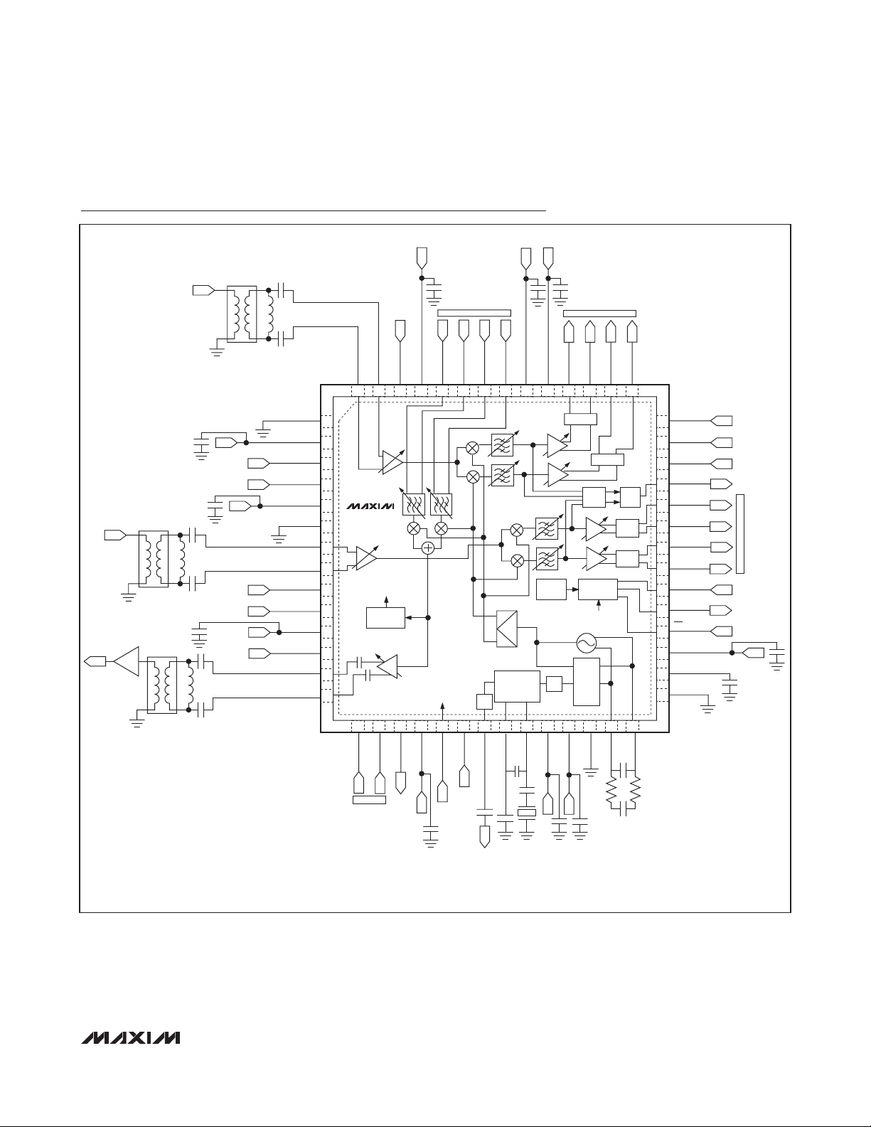
MAX2839AS
2.3GHz to 2.7GHz MIMO Wireless
BroadbandRF Transceiver
______________________________________________________________________________________ 37
Typical Operating Circuit
Rx B INPUT
Tx OUTPUT
Rx A INPUT
Rx/Tx GAIN
CONTROL
CLKOUT
SELECT
Rx/Tx GAIN
CONTROL
Rx/Tx GAIN
CONTROL
Rx/Tx GAIN
CONTROL
GNDRXLNA_A
V
CCRXLNA_A
CLKOUT_DIV
V
CCRXLNA_B
GNDRXLNA_B
RXINB+
RXINB-
V
CCTXPAD
TXOUT+
TXOUT-
MODE
CONTROL
TXRX
RXINA-
RXINA+
63 62 41 61 37 60 59 73 72 32 58 57 31 30
+
1
2
B0
64
38
3
MAX2839AS
39
5
40
B4
9
IMUX/QMUX
B3
8
10
B2
7
43
45
AM
DETECTOR
CCRXMX
V
SERIAL
INTERFACE
TXBBQ-
Tx INPUTS
TXBBQ+
TXBBI+
÷
CCRXFLVCCRXVGA
V
TXBBI-
90°
0°
CRYSTAL
OSCILLATOR/
BUFFER
TEMP
SENSOR
÷
Rx A OUTPUTS
RXBBIA+
IMUX
INTERFACE
PLL
RXBBIA-
QMUX
RSSI
MUX
SERIAL
SCLK
RXBBQA+
RSSI
QMUX
IMUX
RXBBQA-
56
29
71
70
28
69
27
68
53
66
25
23
22
21
RXHP
B6
B7
RSSI
RXBBQB+
RXBBQB-
RXBBIB+
RXBBIB-
DIN
DOUT
CS
V
CCVCO
VCOBYP
GNDVCO
Rx BASBAND
HPF CONTROL
Rx/Tx GAIN
CONTROL
Rx GAIN
CONTROL
Rx B
OUTPUTS
SERIAL
INPUT
SERIAL
OUTPUT
SERIAL
INPUT
44 42 13 46 15 65 47 16 55 17 18 19 20 51
B5
B1
Rx/Tx GAIN
CONTROL
CCTXMX
V
SCLK
SERIAL
INPUT
ENABLE
MODE
CONTROL
REFERENCE
CLOCK
OUTPUT
PABIA S
CLKOUT
REFCLK
XTAL1
CCCP
V
CCXTAL
V
GNDCP
CPOUT+
PLL
FILTER
CPOUT-

MAX2839AS
2.3GHz to 2.7GHz MIMO Wireless
Broadband RF Transceiver
38 ______________________________________________________________________________________
Chip Information
PROCESS: BiCMOS
Bump Configuration
PACKAGE TYPE PACKAGE CODE DOCUMENT NO.
73 WLP W733A5+1
21-0146
Package Information
For the latest package outline information and land patterns, go
to www.maxim-ic.com/packages
. Note that a “+”, “#”, or “-” in
the package code indicates RoHS status only. Package drawings may show a different suffix character, but the drawing pertains to the package regardless of RoHS status.
36 35 34 33
1
62
63
2
3
38
4
39
5
6
7
8
9
10
43
11
12
13
61
64
40
41
MAX2839AS
42
44
45
54
46
47
15
14
31
32
59
60
37
55
16
58 57
73
72
71
69
66
65
49
48
17
30
29
56
70
28
68
27
67
26
53
25
24
23
52
22
50
51
21
18
19
20

MAX2839AS
2.3GHz to 2.7GHz MIMO Wireless
Broadband RF Transceiver
Maxim cannot assume responsibility for use of any circuitry other than circuitry entirely embodied in a Maxim product. No circuit patent licenses are
implied. Maxim reserves the right to change the circuitry and specifications without notice at any time.
Maxim Integrated Products, 120 San Gabriel Drive, Sunnyvale, CA 94086 408-737-7600 ____________________
39
© 2010 Maxim Integrated Products Maxim is a registered trademark of Maxim Integrated Products, Inc.
Revision History
REVISION
NUMBER
0 4/09 Initial release —
1 5/10
REVISION
DATE
DESCRIPTION
Added soldering temperature to Absolute Maximum Ratings; corrected name in
global references to MAX2839AS Evaluation Kit
PAGES
CHANGED
2–18
 Loading...