

Page 1
General Description
The MAX2838 direct-conversion, zero-IF, RF transceiver is designed specifically for 3.3GHz to 3.9GHz wireless broadband systems. The MAX2838 completely
integrates all circuitry required to implement the RF
transceiver function, providing RF-to-baseband receive
path, baseband-to-RF transmit path, VCO, frequency
synthesizer, and baseband/control interface. The
device includes a fast-settling sigma-delta RF synthesizer with smaller than 29Hz frequency steps. The
MAX2838 supports 2Tx, 2Rx MIMO applications with a
master device providing coherent LO to the slave
device. The transceiver IC also integrates circuits for
on-chip DC-offset cancellation, I/Q error, and carrierleakage detection circuits. Only an RF bandpass filter
(BPF), TCXO, RF switch, PA, and a small number of
passive components are needed to form a complete
wireless broadband RF radio solution.
The MAX2838 completely eliminates the need for an
external SAW filter by implementing on-chip monolithic
filters for both the receiver and transmitter. The baseband filters along with the Rx and Tx signal paths are
optimized to meet the stringent noise figure and linearity specifications. The device supports up to 2048-FFT
OFDM and implements programmable channel filters
for 1.5MHz to 28MHz RF channel bandwidths. The
transceiver requires only 2µs Tx-Rx switching time. The
IC is available in a small 48-pin thin QFN package measuring only 6mm x 6mm x 0.8mm.
Applications
802.16-2004/802.16d Fixed WiMAX™
802.16e MIMO Mobile WiMAX
WiMAX Pico and Femto Basestations
NLOS Wireless Broadband Systems
Features
♦ 3.3GHz to 3.9GHz Wide-Band Operation
♦ Master-Slave Modes with Coherent LO for MIMO
♦ Complete RF Transceiver, and PA Driver
0dBm Linear OFDM Transmit Power
-70dBr Tx Spectral Emission Mask
2.8dB Rx Noise Figure
Tx/Rx I/Q Error and LO Leakage Detection and
Adjustment
Automatic Rx DC Offset Correction
Monolithic Low-Noise VCO with -39dBc Integrated
Phase Noise
Programmable Rx I/Q Lowpass Channel Filters
Programmable Tx I/Q Lowpass Anti-Aliasing Filter
Sigma-Delta Fractional-N PLL with 29Hz Step Size
60dB Tx Gain Control Range with 1dB Step Size,
Digitally Controlled
94dB Rx Gain Control Range with 2dB Step Size,
Digitally Controlled
60dB Analog RSSI Instantaneous Dynamic Range
4-Wire SPI™ Digital Interface
I/Q Analog Baseband Interface
Digital Tx/Rx/Shutdown Mode Control
Low-Power CLOCKOUT Mode
On-Chip Digital Temperature Sensor Readout
♦ +2.7V to +3.6V Transceiver Supply
♦ Low-Power Shutdown Mode
♦ Small 48-Pin Thin QFN Package (6mm x 6mm x 0.8mm)
MAX2838
3.3GHz to 3.9GHz
Wireless Broadband RF Transceiver
________________________________________________________________
Maxim Integrated Products
1
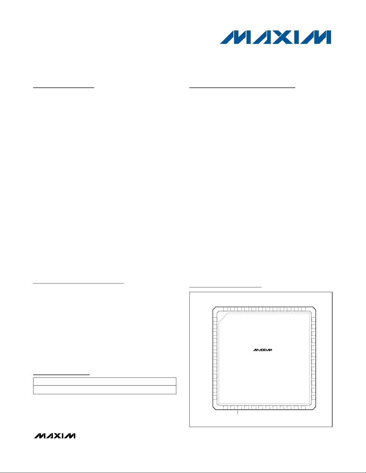
Pin Configuration
Ordering Information
19-1049; Rev 1; 8/08
For pricing, delivery, and ordering information, please contact Maxim Direct at 1-888-629-4642,
or visit Maxim’s website at www.maxim-ic.com.
*
EP = Exposed paddle.
+
Denotes a lead-free package.
T = Tape and reel.
WiMAX is a trademark of the WiMAX Forum.
SPI is a trademark of Motorola, Inc.
PART TEMP RANGE PIN-PACKAGE
M AX 2838E TM + T- 40°C to + 85°C 48 TQ FN - E P *
VCCRXLNA
GNDRXLNA
RXRF+
RXRF-
VCCTXPAD
TXRF+
TXRF-
TXBBI-
TXBBI+
TXBBQ+
TXBBQ-
VCCRXMX
RXTX
ENABLE
48 47 46 45 44 43 42 41 40 39 38 37
+
1
2
3
B5
4
5
6
B4
7
8
B3
B2
9
10
11
12
B1
13 14 15 16 17 18 19 20 21 22 23 24
PABIAS
VCCTMX
MAX2838
CS
SCLK
VCCDIG
CLKOUT
48 THIN QFN
REFCLK
VCCRXFL
VCCCP
RXHP
GNDCP
VCCRXVGA
CPOUT+
RXBBI+
CPOUT-
RXBBI-
GNDVCO
36
35
34
33
32
31
30
29
28
27
26
25
RXBBQ+
RXBBQ-
B6
B7
RSSI
DIN
DOUT
EXTVCO+
EXTVCO-
VCCLO
VCCVCO
VCOBYP
Page 2
MAX2838
3.3GHz to 3.9GHz
Wireless Broadband RF Transceiver
2 _______________________________________________________________________________________
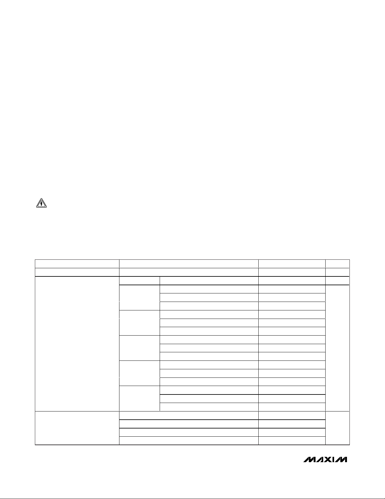
ABSOLUTE MAXIMUM RATINGS
DC ELECTRICAL CHARACTERISTICS
(MAX2838 Evaluation Kit, VCC_ = 2.7V to 3.6V, TA= -40°C to +85°C, ENABLE and RXTX set according to operating mode, CS =
high, SCLK = DIN = low, transmitter and receiver in maximum gain, no input signal at RF inputs, all RF inputs and outputs terminated
into 50Ω, receiver baseband outputs are open. 90mV
RMS
differential I and Q signals (1MHz) applied to I and Q baseband inputs of
transmitter in transmit mode, all registers set to recommended settings and corresponding test mode, unless otherwise noted.
Typical values are at V
CC
= 2.8V, fLO= 3.6GHz, and TA= +25°C, unless otherwise noted.) (Note 1)
Stresses beyond those listed under “Absolute Maximum Ratings” may cause permanent damage to the device. These are stress ratings only, and functional
operation of the device at these or any other conditions beyond those indicated in the operational sections of the specifications is not implied. Exposure to
absolute maximum rating conditions for extended periods may affect device reliability.
V
CC_
Pins to GND..................................................-0.3V to +3.6V
RF Inputs: RXRF+, RXRF-, EXTVCO+,
EXTVCO- to GND ................................................-0.3V to +3.6V
RF Outputs: TXRF+, TXRF-, EXTVCO+,
EXTVCO- to GND ................................................-0.3V to +3.6V
Analog Inputs: TXBBI+, TXBBI-, TXBBQ+,
TXBBQ-, REFCLK to GND ...................................-0.3V to +3.6V
Analog Outputs: RXBBI+, RXBBI-, RXBBQ+,
RXBBQ-, RSSI, VCOBYP, CPOUT+, CPOUT-,
PABIAS to GND ...................................................-0.3V to +3.6V
Digital Inputs: ENABLE, RXTX, CS, SCLK,
DIN, RXHP B1–B7 to GND ..................................-0.3V to +3.6V
Digital Outputs: DOUT, CLKOUT to GND .............-0.3V to +3.6V
Short-Circuit Duration
Analog Outputs: RXBBI+, RXBBI-, RXBBQ+,
RSSI, VCOBYP,RXBBQ-, CPOUT+, CPOUT-,
PABIAS, TXRF-, TXRF+ ......................................................10s
Digital Outputs: DOUT, CLKOUT .........................................10s
RF Input Power: RXRF+, RXRF- .....................................+15dBm
RF Output Differential Load VSWR: TXRF+, TXRF- .................6:1
Continuous Power Dissipation (T
A
= +70°C)
48-Pin Thin QFN (derate 37mW/°C above +70°C) ...... > 2.96W
Operating Temperature Range ...........................-40°C to +85°C
Junction Temperature......................................................+150°C
Storage Temperature Range .............................-65°C to +160°C
Lead Temperature (soldering, 10s) .................................+300°C
CAUTION! ESD SENSITIVE DEVICE
PARAMETERS CONDITIONS MIN TYP MAX UNITS
Supply Voltage V
Supply Current
Rx I/Q Output Common-Mode
Voltage
CC_
S hutd ow n m ode TA = +25°C 12 µA
Standby mode,
see Tables
1 and 2
Rx mode, see
Tables 1 and 2
Tx mode, see
Tables 1 and 2
Rx calibration
mode, see
Tables 1 and 2
Tx calibration
mode, see
Tables 1 and 2
D9:D8 = 00 in A4:A0 = 00100 0.8 1.0 1.2
D9:D8 = 01 in A4:A0 = 00100 1.1
D9:D8 = 10 in A4:A0 = 00100 1.2
D9:D8 = 11 in A4:A0 = 00100 1.35
Single configuration 35 52
MIMO master configuration 44
MIMO slave configuration 11
Single configuration 103 133
MIMO master configuration 112
MIMO slave configuration 80
Single configuration 152 186
MIMO master configuration 160
MIMO slave configuration 128
Single configuration 142 182
MIMO master configuration 151
MIMO slave configuration 119
Single configuration 111 145
MIMO master configuration 120
MIMO slave configuration 88
2.7 2.8 3.6 V
mA
V
Page 3
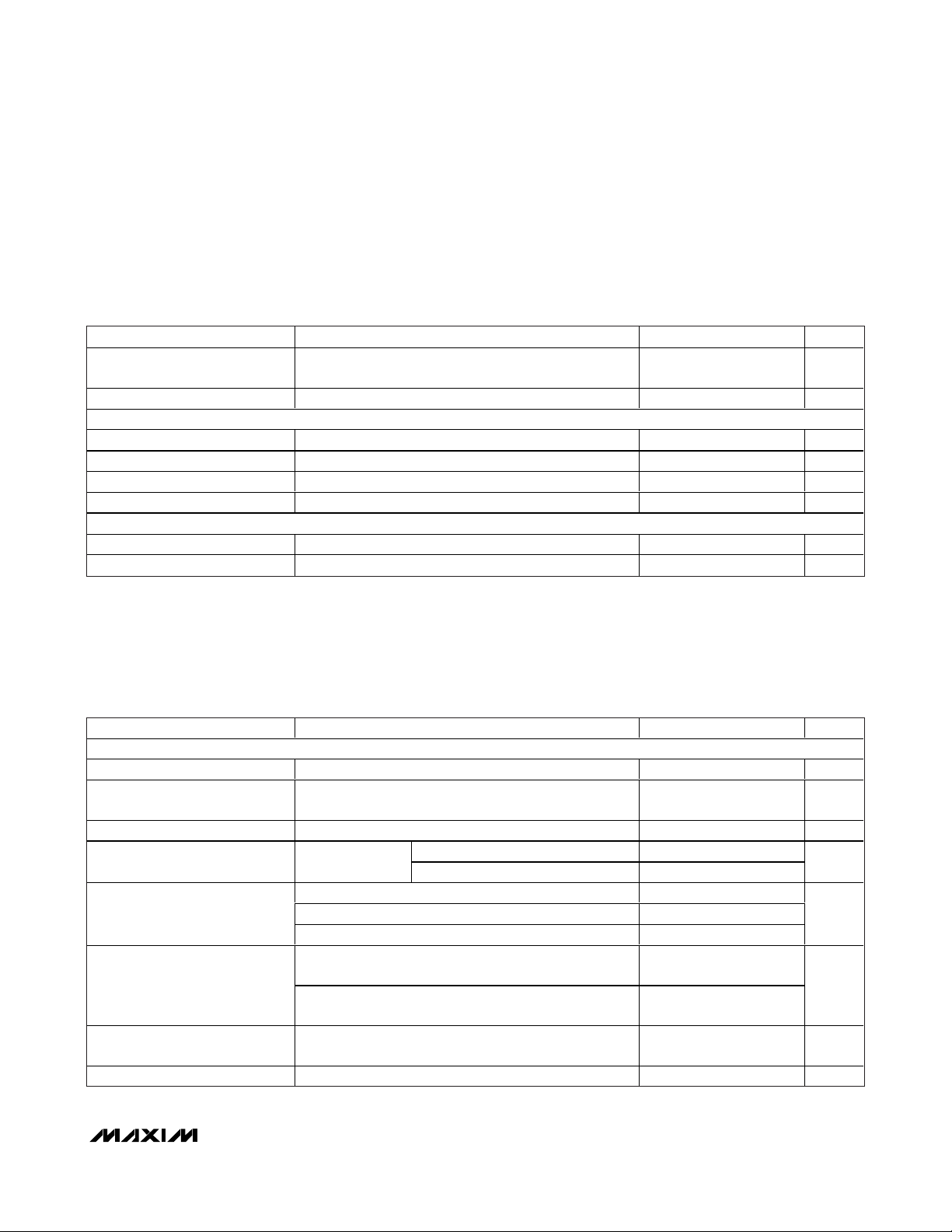
MAX2838
3.3GHz to 3.9GHz
Wireless Broadband RF Transceiver
_______________________________________________________________________________________ 3
AC ELECTRICAL CHARACTERISTICS—Rx MODE
(MAX2838 Evaluation Kit, VCC_ = 2.8V, TA= +25°C, fLO= 3.6GHz, fRF= 3.601GHz, receiver baseband I/Q outputs at 90mV
RMS
, f
REF
= 40MHz, CS = ENABLE = RXTX = high, SCLK = DIN = low, channel bandwidth BW = 7MHz, with power matching for the RF inputs
using the typical applications and registers set to default settings and corresponding test mode, unless otherwise noted.
Unmodulated single-tone RF input signal is used with specifications that normally apply over the entire operating conditions, unless
otherwise indicated. Rx I/Q differential output load impedance = 10kΩ || 8pF.) (Note 1)
DC ELECTRICAL CHARACTERISTICS (continued)
(MAX2838 Evaluation Kit, VCC_ = 2.7V to 3.6V, TA= -40°C to +85°C, ENABLE and RXTX set according to operating mode, CS =
high, SCLK = DIN = low, transmitter and receiver in maximum gain, no input signal at RF inputs, all RF inputs and outputs terminated
into 50Ω, receiver baseband outputs are open. 90mV
RMS
differential I and Q signals (1MHz) applied to I and Q baseband inputs of
transmitter in transmit mode, all registers set to recommended settings and corresponding test mode, unless otherwise noted.
Typical values are at V
CC
= 2.8V, fLO= 3.6GHz, and TA= +25°C, unless otherwise noted.) (Note 1)
PARAMETERS CONDITIONS MIN TYP MAX UNITS
Tx Baseband Input CommonMode Voltage Operating Range
Tx Baseband Input Bias Current Source current 8 20 µA
LOGIC INPUTS: ENABLE, RXTX, SCLK, DIN, CS, B1:B7, RXHP
Digital Input Voltage High, V
Digital Input Voltage Low, V
Digital Input Current High, I
Digital Input Current Low, I
LOGIC OUTPUTS: DOUT
Digital Output Voltage High, V
Digital Output Voltage Low, V
DC-coupled 0.5 1.2 V
IH
IL
IH
IL
Sourcing 100µA V
OH
Sinking 100µA 0.4 V
OL
V
- 0.4 V
C C
0.4 V
-1 +1 µA
-1 +1 µA
- 0.4 V
C C
PARAMETER CONDITIONS MIN TYP MAX UNITS
RECEIVER SECTION: LNA RF INPUT TO BASEBAND I/Q OUTPUTS
RF Input Frequency Range 3.3 3.9 GHz
Peak-to-Peak Gain Variation over
RF Input Frequency Range
RF Input Return Loss All LNA settings 10 dB
Total Voltage Gain TA = -40°C to +85°C
Gain Change Settling Time
Baseband Gain Range
Baseb and Gai n M i ni m um S tep S i ze 2dB
Tested at band edges and band center 1.8 dB
Maximum gain, B7:B1 = 0000000 88 98
Minimum gain, B7:B1 = 1111111 5 10
From max RF gain to max RF Gain - 8dB 8
From max RF gain to max RF gain - 16dB 16RF Gain Steps
From max RF gain to max RF gain - 32dB 32
Any RF or baseband gain change; gain settling to within
±1dB of steady state; RXHP = 1
Any RF or baseband gain change; gain settling to within
±0.1dB of steady state; RXHP = 1
Fr om m axi m um b aseb and g ai n ( B5:B1 = 00000) to m i ni m um
b aseb and g ai n ( B5:B1 = 11111)
200
500
62 dB
dB
dB
ns
Page 4
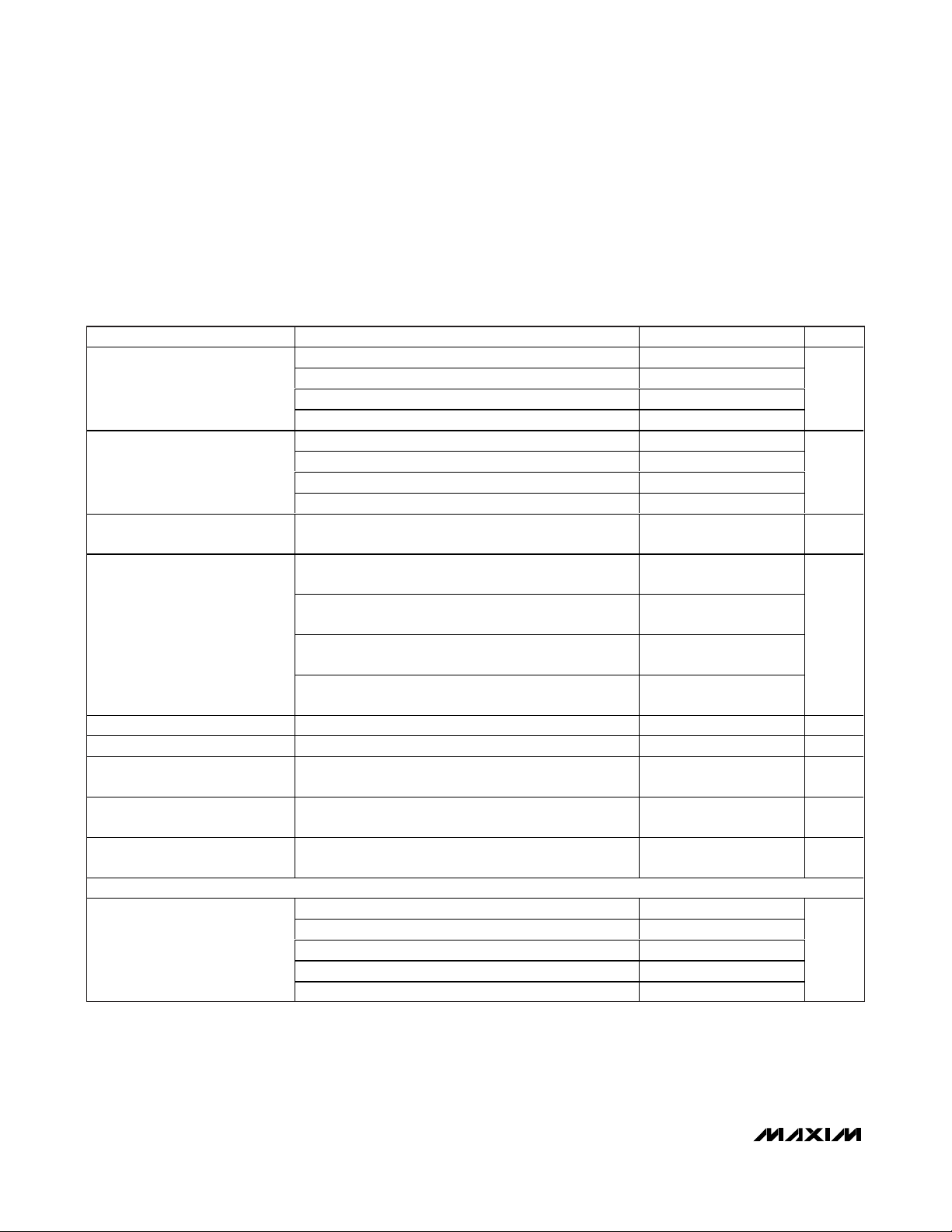
MAX2838
3.3GHz to 3.9GHz
Wireless Broadband RF Transceiver
4 _______________________________________________________________________________________
AC ELECTRICAL CHARACTERISTICS—Rx MODE (continued)
(MAX2838 Evaluation Kit, VCC_ = 2.8V, TA= +25°C, fLO= 3.6GHz, fRF= 3.601GHz, receiver baseband I/Q outputs at 90mV
RMS
, f
REF
= 40MHz, CS = ENABLE = RXTX = high, SCLK = DIN = low, channel bandwidth BW = 7MHz, with power matching for the RF inputs
using the typical applications and registers set to default settings and corresponding test mode, unless otherwise noted.
Unmodulated single-tone RF input signal is used with specifications that normally apply over the entire operating conditions, unless
otherwise indicated. Rx I/Q differential output load impedance = 10kΩ || 8pF.) (Note 1)
PARAMETER CONDITIONS MIN TYP MAX UNITS
DSB Noise Figure
In-Band Input P-1dB
Maximum Output Signal Level
Out-of-Band Input IP3 (Note 2)
I/Q Phase Error 1MHz baseband output; 1 σ variation, TA = +25°C 0.15 D eg r ees
I/Q Gain Imbalance 1MHz baseband output; 1 σ variation, TA = +25°C 0.05 dB
I/Q Output DC Droop
I/Q Static DC Offset
Loopback Gain (for Receiver I/Q
Calibration)
RECEIVER BASEBAND FILTERS
Baseband Highpass Filter Corner
Frequency
Voltage gain ≥ 65dB with max RF gain (B7:B6 = 00) 2.9
V ol tag e g ai n = 50d B w i th m ax RF g ai n - 8d B ( B7:B6 = 01) 7.9
V ol tag e g ai n = 45d B w i th m ax RF g ai n - 16d B ( B7:B6 = 10) 13.7
V ol tag e g ai n = 15d B w i th m ax RF g ai n - 32d B ( B7:B6 = 11) 31.4
Max RF gain (B7:B6 = 00) -35
Max RF gain - 8dB (B7:B6 = 01) -27
Max RF gain - 16dB (B7:B6 = 10) -19
Max RF gain - 32dB (B7:B6 = 11) -3
Over passband frequency range; at any gain setting;
1dB compression point, differential output
Max RF gain (B7:B6 = 00), AGC set for -65dBm wanted
signal
Max RF gain - 8dB (B7:B6 = 01), AGC set for -55dBm
wanted signal
Max RF gain - 16dB (B7:B6 = 10), AGC set for -40dBm
wanted signal
Max RF gain - 32dB (B7:B6 = 11), AGC set for -30dBm
wanted signal
After completion of default power-on on-chip DC
cancellation, 1 σ variation
N o RF i np ut si g nal ; B7:B1 = 0000000, after com p l eti on of
d efaul t p ow er - on on- chi p D C cancel l ati on, 1 σ var i ati on
Tr ansm itter I/Q i nput to r ecei ver I/Q outp ut; tr ansm i tter B6:B1 =
000011, r ecei ver B5:B1 = 10011 p r og r am m ed thr oug h S P I
Corner frequency 1 600
Corner frequency 2 100
Corner frequency 3 30
Corner frequency 4 1
Corner frequency 5 0.1
-7.0 -2 +2.5 dB
2.5 V
-10
-5
-4
+23
±1 V/s
±1.0 mV
dBm
dBm
dB
P-P
kHz
Page 5
MAX2838
3.3GHz to 3.9GHz
Wireless Broadband RF Transceiver
_______________________________________________________________________________________ 5
AC ELECTRICAL CHARACTERISTICS—Rx MODE (continued)
(MAX2838 Evaluation Kit, VCC_ = 2.8V, TA= +25°C, fLO= 3.6GHz, fRF= 3.601GHz, receiver baseband I/Q outputs at 90mV
RMS
, f
REF
= 40MHz, CS = ENABLE = RXTX = high, SCLK = DIN = low, channel bandwidth BW = 7MHz, with power matching for the RF inputs
using the typical applications and registers set to default settings and corresponding test mode, unless otherwise noted.
Unmodulated single-tone RF input signal is used with specifications that normally apply over the entire operating conditions, unless
otherwise indicated. Rx I/Q differential output load impedance = 10kΩ || 8pF.) (Note 1)
PARAMETER CONDITIONS MIN TYP MAX UNITS
A4:A0 = 00010 serial bits D7:D4 = 0000 1.5
A4:A0 = 00010 serial bits D7:D4 = 0001 1.75
A4:A0 = 00010 serial bits D7:D4 = 0010 3.5
A4:A0 = 00010 serial bits D7:D4 = 0011 5.0
A4:A0 = 00010 serial bits D7:D4 = 0100 5.5
A4:A0 = 00010 serial bits D7:D4 = 0101 6.0
A4:A0 = 00010 serial bits D7:D4 = 0110 7.0
RF Channel BW Supported by
Baseband Filter
Baseband Gain Ripple 0 to 3.2MHz for BW = 7MHz 1 dB
Baseband Group Delay Ripple 0 to 3.2MHz for BW = 7MHz 65 ns
Baseband Filter Rejection for
7MHz RF Channel BW
RSSI
RSSI Minimum Output Voltage R
RSSI Maximum Output Voltage R
RSSI Slope 30 mV/dB
RSSI Output Settling Time
A4:A0 = 00010 serial bits D7:D4 = 0111 8.0
A4:A0 = 00010 serial bits D7:D4 = 1000 9.0
A4:A0 = 00010 serial bits D7:D4 = 1001 10.0
A4:A0 = 00010 serial bits D7:D4 = 1010 12.0
A4:A0 = 00010 serial bits D7:D4 = 1011 14.0
A4:A0 = 00010 serial bits D7:D4 = 1100 15.0
A4:A0 = 00010 serial bits D7:D4 = 1101 20.0
A4:A0 = 00010 serial bits D7:D4 = 1110 24.0
A4:A0 = 00010 serial bits D7:D4 = 1111 28.0
At 4.67MHz 7
At > 10.5MHz 53
At > 14MHz 75
At > 29.4MHz 75
≥ 10kΩ 0.65 V
LOAD
≥ 10kΩ 2.4 V
LOAD
To within 3dB of steady
state
+32dB signal step 200
-32dB signal step 800
MHz
dB
ns
P-P
P-P
Page 6
MAX2838
3.3GHz to 3.9GHz
Wireless Broadband RF Transceiver
6 _______________________________________________________________________________________
AC ELECTRICAL CHARACTERISTICS—Tx MODE
(MAX2838 Evaluation Kit, VCC_ = 2.8V, TA= +25°C, fRF= 3.601GHz , fLO= 3.6GHz. f
REF
= 40MHz, ENABLE = CS = high, and RXTX
= SCLK = DIN = low, with power matching for the differential RF pins using the
Typical Operating Circuit
. Lowpass filter is set to
7MHz RF channel BW, 90mV
RMS
sine and cosine signal (or 90mV
RMS
64QAM 1024-FFT OFDMA FUSC I/Q signals wherever OFDM
is mentioned) applied to baseband I/Q inputs of transmitter (differential DC-coupled). Registers set to recommended settings and
corresponding test mode, unless otherwise noted.) (Note 1)
AC ELECTRICAL CHARACTERISTICS—FREQUENCY SYNTHESIS
(MAX2838 Evaluation Kit, VCC= 2.8V, TA= +25°C, fLO= 3.6GHz, f
REF
= 40MHz, CS = high, SCLK = DIN = low, PLL loop bandwidth
= 180kHz, charge-pump comparison frequency = 40MHz, T
A
= +25°C, unless otherwise noted.) (Note 1)
PARAMETER CONDITIONS MIN TYP MAX UNITS
TRANSMIT SECTION: Tx BASEBAND I/Q INPUTS TO RF OUTPUTS
RF Output Frequency Range 3.3 3.9 GHz
Peak-to-Peak Gain Variation over
RF Band
Total Voltage Gain Maximum gain; at unbalanced 50Ω matched output 8 dB
Maximum Output Power over
Frequency
RF Output Return Loss All gain settings 7 dB
RF Gain Control Range 60 dB
RF Gain Control Binary Weights
Unwanted Sideband Suppression
Carrier Leakage Rel ati ve to 0d Bm outp ut p ow er ; w i thout cal i b r ati on b y m od em -40 dBc
Tx I/Q Input Impedance (R || C)
Baseband Frequency Response
for 7MHz RF Channel BW
Baseband Group Delay Ripple 0 to 4.9MHz (BW = 7MHz) 15 ns
O FD M si g nal confor m i ng to sp ectr al em i ssi on m ask and
- 36d B EV M after I/Q i m bal ance cal i br ation by m od em ( N ote 3)
B1 1
B2 2
B3 4
B4 8
B5 16
B6 32
Without calibration by modem, and excludes modem I/Q
imbalance; P
Minimum differential resistance 60 kΩ
Maximum differential capacitance 0.5 pF
0 to 4.67MHz -8
At > 13.23MHz -45
OUT
= 0dBm
2.6 dB
0 dBm
-40 dBc
dB
dB
P-P
PARAMETER CONDITIONS MIN TYP MAX UNITS
FREQUENCY SYNTHESIZER
RF Channel Center Frequency 3.3 3.9 GHz
Channel Center Frequency
Programming Minimum Step Size
Charge-Pump Comparison
Frequency
Reference Frequency Range 11 40 80 MHz
Refer ence Fr eq uency Inp ut Level s AC-coupled to REFCLK pin 800 mV
29 Hz
11 40 MHz
P-P
Page 7
MAX2838
3.3GHz to 3.9GHz
Wireless Broadband RF Transceiver
_______________________________________________________________________________________ 7
AC ELECTRICAL CHARACTERISTICS—FREQUENCY SYNTHESIS (continued)
(MAX2838 Evaluation Kit, VCC= 2.8V, TA= +25°C, fLO= 3.6GHz, f
REF
= 40MHz, CS = high, SCLK = DIN = low, PLL loop bandwidth
= 180kHz, charge-pump comparison frequency = 40MHz, T
A
= +25°C, unless otherwise noted.) (Note 1)
AC ELECTRICAL CHARACTERISTICS—MISCELLANEOUS BLOCKS
(MAX2838 Evaluation Kit, VCC= 2.8V, f
REF
= 40MHz, CS = high, SCLK = DIN = low, and TA= +25°C, unless otherwise noted) (Note 1)
PARAMETER CONDITIONS MIN TYP MAX UNITS
Programmable Reference Divider
Values
Closed-Loop Integrated Phase
Noise
Charge-Pump Output Current On each differential side 0.8 mA
Close-In Spur Level
Reference Spur Level f
Turnaround LO Frequency Error
Temperature Range over which
VCO Maintains Lock
C LKO U T Fr eq uency D i vi d er V al ues A4:A0 = 10100, D6:D5 = 01 ( N ote 4)
CLKOUT Output Swing R = 10kΩ, C = 10pF
External VCO Input Power MIMO slave mode only -10 dBm
External VCO Output Power MIMO master mode only -8 dBm
A4:A0 = 10100, D2:D1 = 00 1
A4:A0 = 10100, D2:D1 = 01 2
Loop BW = 180kHz, integrate phase noise from 200Hz to
5MHz
f
= 0 to 1.8MHz -45
OFFSET
f
= 1.8MHz to 7MHz -70
OFFSET
f
> 7MHz -80
OFFSET
≥ 40MHz -73 dBc
OFFSET
Rel ati ve to stead y state; m easur ed 35µs after Tx- Rx or Rx- Tx
sw i tchi ng i nstant, and 4µs after any r ecei ver g ai n chang es
Rel ati ve to the i ni ti al am b i ent tem p er atur e TA , as l ong as
the fi nal tem p er atur e i s w i thi n op er ati ng tem p er atur e r ang e
-39 dBc
±50 Hz
T
± 40 °C
A
2
Low drive 1.6
High drive 2.4
dBc
V
P-P
PARAMETER CONDITIONS MIN TYP MAX UNITS
PA BIAS DAC: CURRENT MODE
Numbers of bits 6
Minimum Output Sink Current D5:D0 = 000000 in A4:A0 = 11100 0 µA
Maximum Output Sink Current D5:D0 = 111111 in A4:A0 = 11100 310 µA
Compliance Voltage Range 0.8 V
Turn-On Time E xcl ud es p r og r am m ab l e d el ay of 0 to 7µs i n step s of 0.5µs 200 ns
DNL 1 LSB
PA BIAS DAC: VOLTAGE MODE
Output High Level 10mA source current VCC - 0.2 V
Output Low Level 10mA sink current 0.1 V
Turn-On Time E xcl ud es p r og r am m ab l e d el ay of 0 to 7µs i n step s of 0.5µs 200 ns
ON-CHIP TEMPERATURE SENSOR
Temperature Step Size 5°C
Read-out at DOUT pin through SPI
A4:A0 = 00111, D4:D0
TA = +25°C 01111
TA = +85°C 11001Digital Output Code
= -40°C 00100
T
A
Page 8

MAX2838
3.3GHz to 3.9GHz
Wireless Broadband RF Transceiver
8 _______________________________________________________________________________________
Note 1: Min and max limits are guaranteed by test above TA= +25°C and are guaranteed by design and characterization at TA=
-40°C. The power-on register settings are not guaranteed. Recommended register setting must be loaded after V
CC
is supplied.
Note 2: Two tones at +20MHz and +39MHz offset with -35dBm/tone. Measure IM3 at 1MHz.
Note 3: Gain adjusted over max gain and max gain - 3dB.
Note 4: V
CC
rise time (0V to 2.7V) must be less than 1ms.
AC ELECTRICAL CHARACTERISTICS—TIMING
(MAX2838 Evaluation Kit, VCC= 2.8V, fLO= 3.6GHz, f
REF
= 40MHz, CS = high, SCLK = DIN = low, PLL loop bandwidth = 180kHz,
and T
A
= +25°C, unless otherwise noted.) (Note 1)
PARAMETER SYMBOL CONDITIONS MIN TYP MAX UNITS
SYSTEM TIMING
Frequency
Channel Switching Time
Turnaround Time
Tx Turn-On Time (from Standby
Mode)
Tx Tur n- Off Ti m e ( to S tand b y M od e) From Tx-enable falling edge 0.1 µs
Rx Turn-On Time (from Standby
Mode)
Rx Tur n- Off Ti m e ( to S tand b y M od e) From Rx-enable falling edge 0.1 µs
4-WIRE SERIAL INTERFACE TIMING (See Figure 1)
SCLK Rising Edge to CS Falling
Edge Wait Time
Falling Edge of CS to Rising
Edge of First SCLK Time
DIN to SCLK Setup Time t
DIN to SCLK Hold Time t
SCLK Pulse-Width High t
SCLK Pulse-Width Low t
Last Rising Edge of SCLK to
Rising Edge of CS or Clock to
Load Enable Setup Time
CS High Pulse Width t
Ti m e Betw een Ri si ng E d g e of C S
and the N ext Ri si ng E d g e of S C LK
Clock Frequency f
Rise Time t
Fall Time t
SCLK Falling Edge to Valid DOUT t
error
settles to
±50Hz
t
CSO
t
CSS
DS
DH
CH
CL
t
CSH
CSW
t
CS1
CLK
Automatic VCO sub-band selection 2 ms
Manual VCO sub-band selection 56 µs
Measured from Tx or Rx
enable rising edge, signal
settling to within 0.5dB of
steady state
M easur ed fr om Tx enab l e r i si ng ed g e, si g nal
settl i ng to w i thi n 0.5d B of stead y state
M easur ed fr om Rx enab l e r i si ng ed g e, si g nal
settl i ng to w i thi n 0.5d B of stead y state
R
F
D
Rx to Tx 2
Tx to Rx 2
2µs
2µs
6ns
6ns
6ns
6ns
6ns
6ns
6ns
20 ns
6ns
45 MHz
f
/ 10 ns
CLK
f
/ 10 ns
CLK
12.5 ns
µs
Page 9
MAX2838
3.3GHz to 3.9GHz
Wireless Broadband RF Transceiver
_______________________________________________________________________________________
9
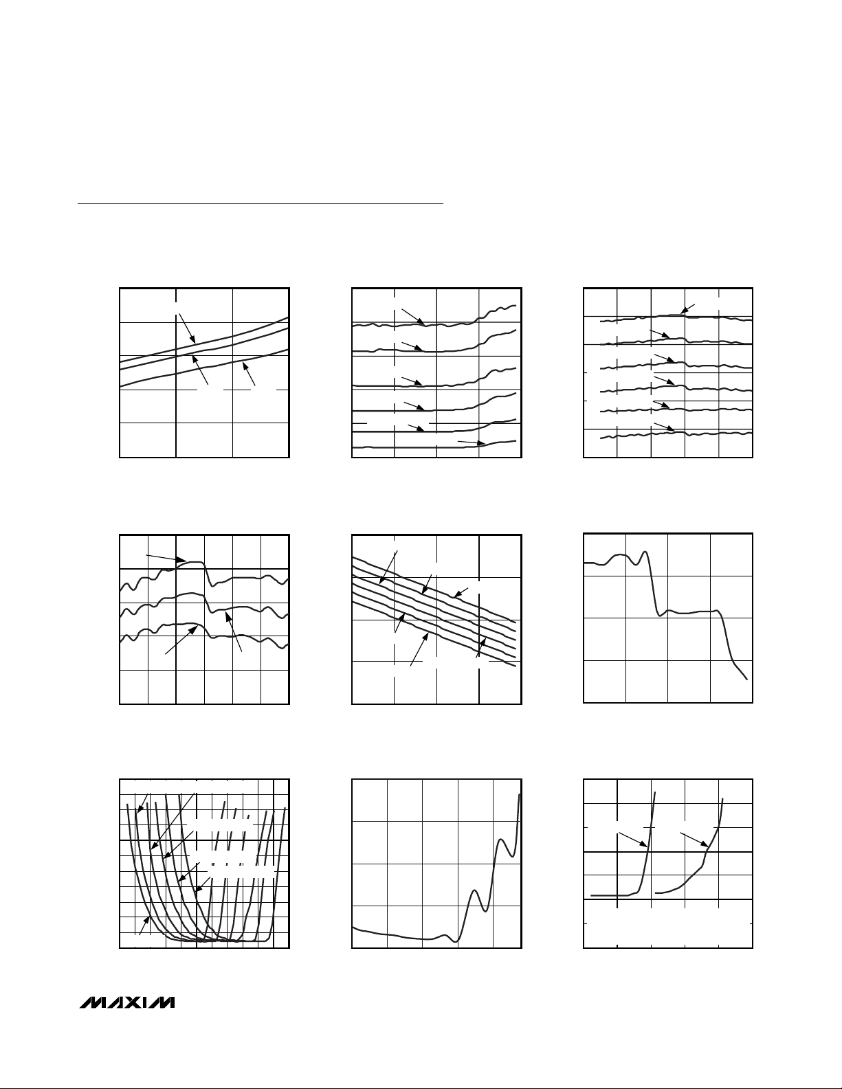
Typical Operating Characteristics
(VCC= 2.8V, TA= +25°C, f
LO
= 3.6GHz, f
REF
= 40MHz, CS = high, RXHP = SCLK = DIN = low, RF BW = 7MHz, using the MAX2838
Evaluation Kit.)
RECEIVER
Rx SUPPLY CURRENT vs. SUPPLY VOLTAGE
105
+85°C
101
97
93
SUPPLY CURRENT (mA)
89
85
2.7 3.3 3.6
+25°C
3.0
SUPPLY VOLTAGE (V)
Rx VOLTAGE GAIN (MAXIMUM LNA GAIN)
vs. FREQUENCY
54
-40°C
52
50
GAIN (dB)
48
46
+85°C
-40°C
+25°C
Rx VOLTAGE GAIN vs. FREQUENCY
60
50
LNA = MAX - 8dB
40
LNA = MAX - 16dB
30
LNA = MAX - 24dB
GAIN (dB)
20
LNA = MAX - 32dB
LNA = MAX - 40dB
10
0
3.0 3.83.4 4.0
FREQUENCY (GHz)
3.63.2
Rx OUTPUT V1dB vs. GAIN SETTING
1.6
1.2
)
RMS
0.8
OUTPUT V1dB (V
0.4
LNA = MAX
MAX2838toc01
NOISE FIGURE (dB)
MAX2838toc03b
VOLTAGE GAIN (dB)
NOISE FIGURE vs. BASEBAND GAIN SETTING
50
LNA = MAX - 40dB
40
LNA = MAX - 32dB
30
LNA = MAX - 24dB
20
LNA = MAX - 16dB
LNA = MAX - 8dB
10
LNA = MAX
0
01632
824
BASEBAND VGA CODE
MAX2838toc02
Rx VOLTAGE GAIN vs. BASEBAND
GAIN SETTING
120
LNA = MAX - 16dB
80
40
LNA = MAX - 32dB
0
LNA = MAX - 40dB
LNA = MAX - 8dB
LNA = MAX
LNA = MAX - 24dB
MAX2838toc04
MAX2838toc03a
MAX2838toc05
44
3.3 3.73.5 3.9
3.63.4 3.8
FREQUENCY (MHz)
Rx EVM vs. PIN (CHANNEL
BANDWIDTH = 10MHz, 64 QAM FUSC)
22
LNA = MAX - 8dB
20
18
16
14
12
10
EVM (%)
8
6
4
2
LNA = MAX
0
-100 -90 -70 -40 -20-50 0-10-30 10
-80 -60
LNA = MAX - 16dB
LNA = MAX - 24dB
LNA = MAX - 32dB
LNA = MAX - 40dB
PIN (dBm)
MAX2838toc06
-40
0 162432
8
BASEBAND VGA CODE
Rx EVM vs. V
(CHANNEL
OUT
BANDWIDTH = 10MHz, 64 QAM FUSC)
16
12
8
EVM (%)
4
0
-30 -15-20
V
OUT
(dBV
RMS
-10-25
)
MAX2838toc07
0
02432
816
BASEBAND VGA CODE
WiMAX EVM vs. OFDM JAMMER
(7MHz CHANNEL BANDWIDTH, 64 QAM FUSC)
14
12
f
10
8
EVM (%)
6
4
2
0
= 7MHz f
OFFSET
P
= P
WANTED
ANTENNA (INCLUDING 4dB FRONT-END LOSS).
EVM AT P
-70 -40 -20
SENSITIVITY
SENSITIVITY
P
JAMMER
= 14MHz
OFFSET
+ 3dB = -71.4dBm AT
= 6%, WITHOUT JAMMER.
at ANTENNA (dBm)
-30-50-60
MAX2838toc08a
Page 10

MAX2838
3.3GHz to 3.9GHz
Wireless Broadband RF Transceiver
10 ______________________________________________________________________________________
Typical Operating Characteristics (continued)
(VCC= 2.8V, TA= +25°C, f
LO
= 3.6GHz, f
REF
= 40MHz, CS = high, RXHP = SCLK = DIN = low, RF BW = 7MHz, using the MAX2838
Evaluation Kit.)
WiMAX EVM vs. OFDM JAMMER
(10MHz CHANNEL BANDWIDTH, 64 QAM FUSC)
MAX2838toc08b
P
JAMMER
AT ANTENNA (dBm)
EVM (%)
-30-50-60
8
10
12
2
4
6
14
0
-70 -40 -20
f
OFFSET
= 10MHz
f
OFFSET
= 20MHz
P
WANTED
= P
SENSITIVITY
+ 3dB = -70.3dBm AT
ANTENNA (INCLUDING 4dB FRONT-END LOSS).
EVM AT P
SENSITIVITY
= 5.85%, WITHOUT JAMMER.
Rx EMISSION SPECTRUM, LNA INPUT
(Tx OFF, LNA = MAX)
MAX2838toc09
0Hz 26.5GHz
(dBm)
-110
-100
-90
-80
-70
-60
-50
-40
-30
-20
-10
Rx INPUT DIFFERENTIAL IMPEDANCE
vs. FREQUENCY
MAX2838toc10
3.3 3.5 3.7
FREQUENCY (GHz)
3.9
REAL COMPONENT (Ω)
IMAGINARY COMPONENT (Ω)
26
30
29
28
27
-75
-55
-60
-65
-70
IMAGINARY
REAL
Rx INPUT RETURN LOSS vs. FREQUENCY
(LNA = MAX)
MAX2838toc11a
30kHz 6.0GHz
(dB)
-50
-40
-30
-20
-10
0
10
20
30
40
50
3.9GHz
3.6GHz
3.3GHz
RSSI VOLTAGE vs. INPUT POWER
MAX2838toc12
PIN (dBm)
RSSI VOLTAGE (V)
1.5
1.0
2.0
2.5
0.5
-100 -40 -10-70
LNA = MAX - 40dB
LNA = MAX - 32dB
LNA = MAX - 24dB
LNA = MAX - 16dB
LNA = MAX - 8dB
LNA = MAX
Rx RSSI STEP RESPONSE
(+40dB SIGNAL STEP)
MAX2838toc13
200ns/div
3V
0V
1.45V
0.45V
LNA GAIN CONTROL
RSSI OUTPUT
Rx RSSI STEP RESPONSE
(-40dB SIGNAL STEP)
MAX2838toc14
200ns/div
3V
0V
1.5V
0.45V
LNA GAIN CONTROL
RSSI
Rx LPF GROUP DELAY vs. FREQUENCY
MAX2838toc15
FREQUENCY (MHz)
LPF GROUP DELAY (ns)
200
300
250
50
150
100
350
0
0 6 12 1610 1424 8
CHANNEL BW = 5MHz
CHANNEL BW = 8MHz
CHANNEL BW = 9MHz
CHANNEL BW = 10MHz
Rx INPUT RETURN LOSS vs. FREQUENCY
(LNA = MAX - 32dB)
MAX2838toc11b
30kHz 6.0GHz
(dB)
-50
-40
-30
-20
-10
0
10
20
30
40
50
3.9GHz
3.6GHz
3.3GHz
Page 11

MAX2838
3.3GHz to 3.9GHz
Wireless Broadband RF Transceiver
______________________________________________________________________________________
11
Typical Operating Characteristics (continued)
(VCC= 2.8V, TA= +25°C, f
LO
= 3.6GHz, f
REF
= 40MHz, CS = high, RXHP = SCLK = DIN = low, RF BW = 7MHz, using the MAX2838
Evaluation Kit.)
Rx DC OFFSET SETTLING RESPONSE
(+8dB BB VGA GAIN STEP)
MAX2838toc16
10μs/div
2V/div
10mV/div
VGA GAIN CONTROL
Rx DC OFFSET SETTLING RESPONSE
(-8dB BB VGA GAIN STEP)
MAX2838toc17
10μs/div
2V/div
10mV/div
VGA GAIN CONTROL
Rx DC OFFSET SETTLING RESPONSE
(-16dB BB VGA GAIN STEP)
MAX2838toc18
10μs/div
2V/div
10mV/div
VGA GAIN CONTROL
Rx DC OFFSET SETTLING RESPONSE
(-32dB BB VGA GAIN STEP)
MAX2838toc19
10μs/div
2V/div
10mV/div
VGA GAIN CONTROL
Rx BBVGA SETTLING RESPONSE
(+8dB GAIN STEP)
MAX2838toc20
200ns/div
100mV/div
2V/div
VGA GAIN CONTROL
Rx BBVGA SETTLING RESPONSE
(-8dB BB VGA GAIN STEP)
MAX2838toc21
200ns/div
100mV/div
2V/div
VGA GAIN CONTROL
Rx BBVGA SETTLING RESPONSE
(-16dB GAIN STEP)
MAX2838toc22
200ns/div
500mV/div
2V/div
VGA GAIN CONTROL
Rx BBVGA SETTLING RESPONSE
(-32dB GAIN STEP)
MAX2838toc23
200ns/div
1V/div
2V/div
VGA GAIN CONTROL
Rx LNA SETTLING RESPONSE
(MAX TO MAX - 8dB)
MAX2838toc24
1μs/div
500mV/div
2V/div
LNA GAIN CONTROL
Page 12

MAX2838
3.3GHz to 3.9GHz
Wireless Broadband RF Transceiver
12 ______________________________________________________________________________________
Typical Operating Characteristics (continued)
(VCC= 2.8V, TA= +25°C, f
LO
= 3.6GHz, f
REF
= 40MHz, CS = high, RXHP = SCLK = DIN = low, RF BW = 7MHz, using the MAX2838
Evaluation Kit.)
TRANSMITTER
Rx LNA SETTLING RESPONSE
(MAX TO MAX - 16dB)
500mV/div
2V/div
474
395
316
237
158
LNA GAIN CONTROL
HISTOGRAM: IQ GAIN IMBALANCE
1μs/div
DEV = 51.8mV
SAMPLE SIZE = 7839
MEAN = 0
MAX2838toc25
MAX2838toc28
Rx BB FREQUENCY RESPONSE
10
0
-10
-20
-30
RESPONSE (dB)
-40
-50
-60
-70
FREQUENCY (MHz)
HISTOGRAM: Rx PHASE IMBALANCE
774
MEAN = 0
DEV = 0.11878°
645
SAMPLE SIZE = 7841
516
387
258
Rx BB FREQUENCY RESPONSE
2
MAX2838toc26
10 1000.1 1
1
0
-1
-2
RESPONSE (dB)
-3
-4
-5
-6
10 1000.1 1
FREQUENCY (MHz)
MAX2838toc27
HISTOGRAM: Rx STATIC DC OFFSET
996
MEAN = 0
DEV = 0.23981mV
MAX2838toc29
830
SAMPLE SIZE = 7841
664
498
332
MAX2838toc30
79
1σ/div
129
1σ/div
166
POWER-ON DC OFFSET CANCELLATION
WITH INPUT SIGNAL
2V/div
200mV/div
ENABLE
MAX2838toc31a
4.00μs/div
POWER-ON DC OFFSET CANCELLATION
WITHOUT INPUT SIGNAL
2V/div
10mV/div
2μs/div
ENABLE
Tx SUPPLY CURRENT vs. SUPPLY VOLTAGE
160
MAX2838toc31b
157
154
151
SUPPLY CURRENT (mA)
148
145
+85°C
1σ/div
MAX2838toc32
-40°C
+25°C
3.3 3.62.7 3.0
Page 13

MAX2838
3.3GHz to 3.9GHz
Wireless Broadband RF Transceiver
______________________________________________________________________________________
13
Typical Operating Characteristics (continued)
(VCC= 2.8V, TA= +25°C, f
LO
= 3.6GHz, f
REF
= 40MHz, CS = high, RXHP = SCLK = DIN = low, RF BW = 7MHz, using the MAX2838
Evaluation Kit.)
Tx BASEBAND FREQUENCY RESPONSE
10
0
CHANNEL BW = 20MHz
-10
-20
CHANNEL BW = 12MHz
-30
-40
RESPONSE (dB)
CHANNEL BW = 1.75MHz
-50
CHANNEL BW = 1.5MHz
-60
CHANNEL BW = 5MHz
-70
0.1 10 1001
CHANNEL BW = 28MHz
FREQUENCY (MHz)
Tx OUTPUT POWER vs. GAIN SETTING
10
-10
(dBm)
-30
OUT
P
-50
-40°C
+85°C
+25°C
MAX2838toc33
MAX2838toc35
10dB/div
Tx BASEBAND FREQUENCY RESPONSE
2
1
0
-1
-2
-3
RESPONSE (dB)
-4
-5
-6
0.1 10 1001
FREQUENCY (MHz)
Tx OUTPUT SPECTRUM
P
= 0dBm
OUT
MAX2838toc33a
MAX2838toc36
MASK
Tx OUTPUT POWER vs. FREQUENCY
4
2
0
(dBm)
-2
OUT
P
-4
-6
-8
3300 3700 39003400 36003500 3800
TX GAIN SET TO MAX - 3dB
-40°C
+25°C
FREQUENCY (MHz)
+85°C
Tx CARRIER SUPPRESSION vs. FREQUENCY
-35
-40
-45
-50
CS (dBc)
-55
-60
-65
TX GAIN SET TO MAX - 3dB
+85°C
-40°C
+25°C
MAX2838toc34
MAX2838toc37
-70
0643216 48
TX GAIN CODE
Tx CARRIER SUPPRESSION vs.
GAIN SETTING
-20
-25
-30
-35
-40
-45
CS (dBc)
-50
-55
-60
-65
-70
-40°C
06432 4816
TX GAIN CODE
-70
3.625GHz3.583GHz
3300 3700 39003400 36003500 3800
FREQUENCY (MHz)
Tx SIDEBAND SUPPRESSION vs.
+85°C
+25°C
MAX2838toc38
Tx SIDEBAND SUPPRESSION vs. FREQUENCY
-30
-40
-50
-60
SS (dBc)
-70
+85°C
-80
-90
3300 3700 39003400 36003500 3800
TX GAIN SET TO MAX - 3dB
-40°C
FREQUENCY (MHz)
+25°C
MAX2838toc39
-30
-40
-50
SS (dBc)
-60
-70
-80
0705030 6010 4020
GAIN SETTING
+85°C
-40°C
+25°C
TX GAIN CODE
MAX2838toc40
Page 14

MAX2838
3.3GHz to 3.9GHz
Wireless Broadband RF Transceiver
14 ______________________________________________________________________________________
Typical Operating Characteristics (continued)
(VCC= 2.8V, TA= +25°C, f
LO
= 3.6GHz, f
REF
= 40MHz, CS = high, RXHP = SCLK = DIN = low, RF BW = 7MHz, using the MAX2838
Evaluation Kit.)
EVM vs. Tx OUTPUT POWER (64 QAM
FUSC, 10MHz CHANNEL BANDWIDTH)
MAX2838toc41
P
OUT
(dBm)
EVM (%)
1.6
0.8
1.2
0.4
2.0
0
-40 -10 0-30 -20
Tx OUTPUT EMISSION SPECTRUM
MAX2838toc42
(dBm)
-10
-50
-30
-70
10
-90
0
-40
-20
-60
-80
0Hz 26.5GHz
f
LO
fLO / 3
f
LO
x 4/3
fLO x 2
HISTOGRAM: Tx LO LEAKAGE
MAX2838toc43
1σ/div
248
310
62
186
124
372
MEAN = -46.235dBc
DEV = 5.1577dB
SAMPLE SIZE = 7841
HISTOGRAM: Tx SIDEBAND SUPPRESSION
MAX2838toc44
1σ/div
336
420
84
252
168
504
MEAN = -47.856dBc
DEV = 2.8827dB
SAMPLE SIZE = 7841
Tx OUTPUT RETURN LOSS vs. FREQUENCY
MAX2838toc45
(dB)
30
-10
10
-30
50
-50
40
0
20
-20
-40
30kHz 6.0GHz
3.9GHz
3.6GHz
3.3GHz
LO FREQUENCY vs.
DIFFERENTIAL TUNE VOLTAGE
MAX2838toc46
DIFFERENTIAL TUNE VOLTAGE (V)
LO FREQUENCY (GHz)
4.0
3.6
3.8
3.4
3.2
4.2
3.0
0 1.51.0 2.52.00.5
PHASE NOISE vs. OFFSET FREQUENCY
MAX2838toc47
OFFSET FREQUENCY (MHz)
PHASE NOISE (dBc/Hz)
-50
-60
-70
-80
-90
-100
-110
-120
-130
-140
-150
0.0001 0.10.01 1010.001
VCO GAIN vs. DIFFERENTIAL TUNE VOLTAGE
MAX2838toc48
DIFFERENTIAL TUNE VOLTAGE (V)
VCO GAIN (MHz/V)
200.00
180.00
160.00
140.00
120.00
100.00
80.00
60.00
40.00
20.00
0.00
0 1.51.0 2.52.00.5
CHANNEL-SWITCHING FREQUENCY SETTLING
(3.3GHz TO 3.9GHz, MANUAL VCO SUB-BAND SELECTION)
MAX2838toc49a
99.69
TIME (μs)
0
10kHz/div
-50kHz
50kHz
SYNTHESIZER
Page 15

MAX2838
3.3GHz to 3.9GHz
Wireless Broadband RF Transceiver
______________________________________________________________________________________
15
Typical Operating Characteristics (continued)
(VCC= 2.8V, TA= +25°C, f
LO
= 3.6GHz, f
REF
= 40MHz, CS = high, RXHP = SCLK = DIN = low, RF BW = 7MHz, using the MAX2838
Evaluation Kit.)
CHANNEL-SWITCHING FREQUENCY SETTLING
(3.9GHz TO 3.3GHz, MANUAL VCO SUB-BAND SELECTION)
MAX2838toc49b
99.69
TIME (μs)
0
10kHz/div
-50kHz
50kHz
CHANNEL-SWITCHING FREQUENCY SETTLING
(3.3GHz TO 3.9GHz, AUTOMATIC VCO
50kHz
SUB-BAND SELECTION)
CHANNEL-SWITCHING FREQUENCY SETTLING
(3.9GHz TO 3.3GHz, AUTOMATIC VCO
SUB-BAND SELECTION)
0
MAX2838toc50
2V/div
MAX2838toc49c
TIME (ms)
1.998
Tx-TO-Rx TURNAROUND FREQUENCY
GLITCH SETTLING
RXTX
2V/div
MAX2838toc49d
50kHz
10kHz/div
-50kHz
Rx-TO-Tx TURNAROUND FREQUENCY
GLITCH SETTLING
RXTX
MAX2838toc51
10kHz/div
-50kHz
0
TIME (ms)
1.998
1kHz/div
FREQUENCY ERROR
4μs/div
1kHz/div
FREQUENCY ERROR
4μs/div
Page 16

MAX2838
3.3GHz to 3.9GHz
Wireless Broadband RF Transceiver
16 ______________________________________________________________________________________
Typical Operating Circuit
RX INPUT
TX OUTPUT
RX/TX GAIN
RX/TX GAIN
CONTROL
RX/TX GAIN
CONTROL
RX/TX GAIN
CONTROL
RX/TX GAIN
CONTROL
CONTROL
VCCRXLNA
GNDRXLNA
RXRF+
RXRF-
VCCTXPAD
TXRF+
TXRF-
TXBBI-
VCCRXFL
RSSI
÷
RX BASEBAND
HPF CONTROL
MODE
CONTROL
TXBBI+
TXBBQ+
TXBBQ-
VCCRXMX
RXTX
ENABLE
48 47 46 45 44 43 42 41 40 39 38
1
2
B5
3
4
5
B4
6
7
IMUX/QMUX
B3
8
B2
B1
AM
9
DETECTOR
10
11
12
SERIAL INTERFACE
MAX2838
REFERENCE
BUFFER
90°
0°
RXHP
VCCRXVGA
TO
RSSI
MUX
TEMP SENSOR
RSSI
SERIAL
INTERFACE
CS SCLK
PLL
RX I OUTPUTSTX INPUT
RXBBI+
IMUX
RXBBI37
QMUX
RSSI
MUX
36
35
34
33
32
31
30
29
28
27
26
25
RXBBQ+
RXBBQ-
B6
B7
RSSI
DIN
DOUT
EXTVCO+
EXTVCO-
VCCLO
VCCVCO
VCOBYP
RX Q
OUTPUTS
RX/TX GAIN
CONTROL
RX GAIN
CONTROL
SERIAL
INPUTS
SERIAL
INPUTS
EXTERNAL
VCO INPUT
OR OUTPUT
GNDVCO
13 14 15 16 17 18 19 20 21 22 23 24
PABIAS
VCCTXMX
SERIAL
INPUTS
CS
SCLK
SERIAL
INPUTS
REFERENCE
CLOCK BUFFER
CLKOUT
OUTPUT
VCCDIG
REFERENCE
REFCLK
CLOCK
INPUT
VCCCP
GNDCP
CPOUT+
PLL LOOP
FILTER
CPOUT-
GNDVCO
Page 17

MAX2838
3.3GHz to 3.9GHz
Wireless Broadband RF Transceiver
______________________________________________________________________________________ 17
Pin Description
PIN NAME FUNCTION
1 VCCRXLNA LNA Supply Voltage. Bypass with a capacitor as close as possible to the pin.
2 GNDRXLNA LNA Ground
3 B5 Receiver and Transmitter Gain-Control Logic Input Bit 5
4 RXRF+
5 RXRF-
6 B4 Receiver and Transmitter Gain-Control Logic Input Bit 4
7 VCCTXPAD Supply Voltage for Power-Amplifier Driver. Bypass with a capacitor as close as possible to the pin.
8 B3 Receiver and Transmitter Gain-Control Logic Input Bit 3
9 B2 Receiver and Transmitter Gain-Control Logic Input Bit 2
10 TXRF+
11 TXRF-
12 B1 Receiver and Transmitter Gain-Control Logic Input Bit 1
13 PABIAS Transmit PA Bias DAC Output
14 VCCTXMX Transmitter Upconverter Supply Voltage. Bypass with a capacitor as close as possible to the pin.
15 CS Chip-Select Logic Input of 4-Wire Serial Interface (See Figure 1)
16 SCLK Serial-Clock Logic Input of 4-Wire Serial Interface (See Figure 1)
17 CLKOUT Reference Clock Divided Output
18 VCCDIG Digital Circuit Supply Voltage. Bypass with a capacitor as close as possible to the pin.
19 REFCLK Reference Clock Input
20 VCCCP PLL Charge-Pump Supply Voltage. Bypass with a capacitor as close as possible to the pin.
21 GNDCP Charge-Pump Circuit Ground
22 CPOUT+
23 CPOUT-
24 GNDVCO VCO Ground
25 VCOBYP
26 VCCVCO VCO Supply Voltage. Bypass with a capacitor as close as possible to the pin.
27 VCCLO LO Generation Supply Voltage. Bypass with a capacitor as close as possible to the pin.
28 EXTVCO-
29 EXTVCO+
30 DOUT Data Logic Output of 4-Wire Serial Interface (See Figure 1)
31 DIN Data Logic Input of 4-Wire Serial Interface (See Figure 1)
32 RSSI RSSI or Temperature Sensor Multiplexed Analog Output
33 B7 Receiver Gain-Control Logic Input Bit 7
34 B6 Receiver and Transmitter Gain-Control Logic Input Bit 6
35 RXBBQ-
36 RXBBQ+
37 RXBBI-
38 RXBBI+
39 VCCRXVGA Receiver VGA Supply Voltage. Bypass with a capacitor as close as possible to the pin.
LNA Differential Inputs. Inputs are internally DC-coupled. Two external series capacitors and one
shunt inductor match the inputs to 100Ω differential.
Power-Amplifier Driver Differential Output. Outputs are internally DC-coupled. Two external series
capacitors and one shunt inductor match the outputs to 100Ω differential.
Differential Charge-Pump Output. Connect the frequency synthesizer’s loop filter between CPOUT+
and CPOUT- (see the Typical Operating Circuit).
On-Chip VCO Regulator Output Bypass. Bypass with a 1µF capacitor to GND. Do not connect other
circuitry to this point.
External VCO Differential Input or Output. Input for slave configuration and output for master
configuration. Leave unconnected for single configuration.
Receiver Baseband Q-Channel Differential Outputs. In Tx calibration mode, these pins are the LO
leakage and sideband detector outputs.
Receiver Baseband I-Channel Differential Outputs. In Tx calibration mode, these pins are the LO
leakage and sideband detector outputs.
Page 18

MAX2838
3.3GHz to 3.9GHz
Wireless Broadband RF Transceiver
18 ______________________________________________________________________________________
Pin Description (continued)
Table 1. Operating Mode for MIMO Master and Single Configuration (Note 5)
Note 5: Set SPI Reg 24 D1:D0 = “00” for single-transceiver mode of operation. Set SPI Reg 16 D4:D3 = “11,” Reg 24 D8 = “1,” Reg
24 D1:D0 = “01” for MIMO master configuration.
Note 6: Unused states of SPI Reg 16, D1:D0 above are not tested, and therefore, should not be used.
Note 7: Parts of transceiver may be selectively enabled.
Note 8: PA bias DAC may be kept active in these non-transmit mode(s) by SPI programming.
Note 9: Set SPI Reg 5 D5 = “1” to mux AM detector output to RXBB pins.
Note 10: Set SPI Reg 26 D3 = “1.”
Note 11: CLKOUT signal is active independent of the states of SPI Reg 16, D1:D0, and is only dependent on the states of ENABLE
and RXTX pins. However, to ensure that the rest of the chip is off when the CLKOUT is active in the clock-out mode, set SPI
Reg 16, D1:D0 to “00” as shown above.
PIN NAME FUNCTION
40 RXHP
41 VCCRXFL Receiver Baseband Filter Supply Voltage. Bypass with a capacitor as close as possible to the pin.
42 TXBBI-
43 TXBBI+
44 TXBBQ+
45 TXBBQ-
46 VCCRXMX Receiver Downconverters Supply Voltage. Bypass with a capacitor as close as possible to the pin.
47 RXTX Mode Control Logic Input. See Table 1 for operating modes.
48 ENABLE Mode Control Logic Input. See Table 1 for operating modes.
—EP
MODE
SHUTDOWN xx 0 0 Off Off Off Off None
STANDBY (Note 7) 01 0 1 Off Off On On None
CLOCK OUT 00 (Note 11) 0 1 Off Off Off On None
Rx 01 1 1 On Off ( N ote 8) On On None
Tx 01 1 0 Off On On On None
Tx CALIBRATION
(Note 9)
Rx CALIBRATION
(Note 10)
Receiver Baseband AC-Coupling Highpass Corner Frequency Control Logic Input. Connect to
ground if not being used.
Transmitter Baseband I-Channel Differential Inputs
Transmitter Baseband Q-Channel Differential Inputs
Exposed Paddle. Connect to the ground plane with multiple vias for proper operation and heat
dissipation. Do not share with any other pin grounds and bypass capacitors’ ground.
MODE CONTROL LOGIC INPUTS CIRCUIT BLOCK STATES
SPI REG 16,
D1:D0 (Note 6)
11 1 0 Off
11 1 1
ENABLE
PIN
RXTX PIN Rx PATH Tx PATH PLL, VCO
On
On
(except
LNA)
(except PA
driver)
On
(except PA
driver)
On On
On On Loopback
CLOCK
OUT
CALI-
BRATION
SEC T I O N S
ON
AM d etector
+ RX I,Q
b uffer s
Page 19

MAX2838
3.3GHz to 3.9GHz
Wireless Broadband RF Transceiver
______________________________________________________________________________________ 19
Detailed Description
Configurations
The MAX2838 can be configured in a) single mode, for
non-MIMO or SISO applications, b) MIMO master
mode, and c) MIMO slave mode. Options b) and c) are
for MIMO applications where a coherent LO is required
for all transmitters and all receivers.
Modes of Operation
The modes of operation for the MAX2838 are clock-out,
shutdown, standby, Tx, Rx, Tx calibration, and Rx calibration. See Table 1 for a summary of the modes of
operation. The logic input pins—RXTX (pin 47) and
ENABLE (pin 48)—control the various modes.
Shutdown Mode (Complete IC Power-Down)
All circuit blocks are powered down, except the 4-wire
serial bus and its internal programmable registers.
Current drain is the minimum possible with the supply
voltages applied. If the digital supply voltage is applied
at the VCCDIG pin, the registers can be loaded.
Standby Mode
PLL, VCO, and LO generation blocks are ON, so that
Tx or Rx modes can be quickly enabled from this
mode. These and other blocks may be selectively
enabled in this mode.
Rx Mode
All Rx circuit blocks are powered on and active.
Antenna signal is applied; RF is downconverted, filtered, and buffered at Rx BB I & Q outputs.
Tx Mode
All Tx circuit blocks are powered on. The external PA is
powered on after a programmable delay.
Clock-Out Only
Only the clock-out signal is active on the CLKOUT pin.
The clock output divider is also functional. The rest of
the transceiver is powered down.
Rx Calibration
Part of the Rx and Tx circuit blocks except the LNA and
PA driver are powered on and active. The transmitter
IQ input signal is upconverted to RF and at the output
of the Tx gain control (VGA). It is fed to the receiver at
the input of the downconverter. Either or both of the two
receiver channels can be connected to the transmitter
and powered on. The I/Q lowpass filters are not present
in the transmitter signal path (they are bypassed).
Tx Calibration
All Tx circuit blocks except the PA driver and external
PA are powered on and active. The AM detector and
receiver I/Q channel buffers are also on, along with
multiplexers in receiver side to route this AM detector’s
signal to each I and Q differential lines.
Table 2. Operating Mode for MIMO Slave Configuration (Note 12)
Note 12: Set SPI Reg 16 D4:3 = “00,” Reg 24 D8 = “0,” Reg 24 D1:0 = “10” to select the MIMO slave configuration.
MODE CONTROL LOGIC INPUTS CIRCUIT BLOCK STATES
C A L I-
MODE
SHUTDOWN xx 0 0 Off Off Off Off None
STANDBY (Note 7) 01 0 1 Off Off Off On None
CLOCK OUT 00 (Note 11) 0 1 Off Off Off On None
Rx 01 1 1 On Off ( N ote 8) Off On None
Tx 01 1 0 Off On Off On None
Tx CALIBRATION
(Note 9)
Rx CALIBRATION
(Note 10)
SPI REG 16,
D1:D0 (Note 4)
11 1 0 Off
11 1 1
ENABLE
PIN
RXTX PIN Rx PATH Tx PATH PLL, VCO
On
On
(except
LNA)
(except PA
driver)
On
(except PA
driver)
Off On
Off On Loop-back
CLOCK
OUT
B R A T I O N
SEC T I O N S
AM d etector
+ RX I,Q
b uffer s
O N
Page 20

MAX2838
3.3GHz to 3.9GHz
Wireless Broadband RF Transceiver
20 ______________________________________________________________________________________
Programmable Registers and
4-Wire SPI-Interface
The MAX2838 includes 32 programmable 16-bit registers. The most significant bit (MSB) is the read/write
selection bit. The next 5 bits are register addresses.
The 10 least significant bits (LSBs) are register data.
Register data is loaded through the 4-wire
SPI/MICROWIRE™-compatible serial interface. Data at
the DIN pin is shifted in MSB first and is framed by CS.
When CS is low, the clock is active, and input data is
shifted at the rising edge of the clock. During the read
mode, register data selected by address bits is shifted
out to the DOUT pin at the falling edges of the clock. At
CS rising edge, the 10-bit data bits are latched into the
register selected by address bits. See Figure 1.
MICROWIRE is a trademark of National Semiconductor Corp.
Chip Information
PROCESS: BiCMOS
DIN
SCLK
CS
DOUT
DIN
SCLK
CS
DOUT
Figure 1. 4-Wire SPI Serial-Interface Timing Diagram
BIT 1
DON’T CARE
BIT 6BIT 2
BIT 14BIT 13BIT 5
t
CH
t
t
CSOtCSS
BIT 1
DS
BIT 2
t
DH
DON’T CARE
SPI REGISTER WRITE
BIT 5
SPI REGISTER READ
t
CL
BIT 6 BIT 14BIT 13
t
D
DON’T CARE
t
CSH
t
CSW
t
CS1
Page 21

MAX2838
3.3GHz to 3.9GHz
Wireless Broadband RF Transceiver
______________________________________________________________________________________ 21
Package Information
For the latest package outline information and land patterns, go to www.maxim-ic.com/packages.
PACKAGE TYPE PACKAGE CODE DOCUMENT NO.
48 TQFN-EP T4866+2
21-0141
Page 22

MAX2838
3.3GHz to 3.9GHz
Wireless Broadband RF Transceiver
Maxim cannot assume responsibility for use of any circuitry other than circuitry entirely embodied in a Maxim product. No circuit patent licenses are
implied. Maxim reserves the right to change the circuitry and specifications without notice at any time.
22
____________________Maxim Integrated Products, 120 San Gabriel Drive, Sunnyvale, CA 94086 408-737-7600
© 2008 Maxim Integrated Products is a registered trademark of Maxim Integrated Products, Inc.
Revision History
REVISIO N
NUMBER
0 10/07 Initial release —
1 8/08
REVISIO N
DATE
DESCRIPTION
Removed CLKOUT frequency divide-by-1 ratio in AC Electrical
Characteristics—Frequency Synthesis table
PAGES
CHANGED
7
 Loading...