

Page 1
General Description
The MAX2831/MAX2832 direct conversion, zero-IF, RF
transceivers are designed specifically for 2.4GHz to
2.5GHz 802.11g/b WLAN applications. The MAX2831
completely integrates all circuitry required to implement
the RF transceiver function, providing an RF power
amplifier (PA), RF-to-baseband receive path, basebandto-RF transmit path, VCO, frequency synthesizer, crystal
oscillator, and baseband/control interface. The MAX2832
integrates the same functional blocks except for the PA.
Both devices include a fast-settling sigma-delta RF synthesizer with smaller than 20Hz frequency steps and a
digitally tuned crystal oscillator allowing use of a low-cost
crystal. The devices also integrate on-chip DC-offset
cancellation and I/Q errors and carrier leakage-detection
circuits. Only an RF bandpass filter (BPF), crystal, RF
switch, and a small number of passive components are
needed to form a complete 802.11g/b WLAN RF frontend solution.
The MAX2831/MAX2832 completely eliminate the need
for an external SAW filter by implementing on-chip monolithic filters for both the receiver and transmitter. The
baseband filters are optimized to meet the IEEE 802.11g
standard and proprietary turbo modes up to 40MHz
channel bandwidth. These devices are suitable for the full
range of 802.11g OFDM data rates (6Mbps to 54Mbps)
and 802.11b QPSK and CCK data rates (1Mbps to
11Mbps). The ICs are available in a small, 48-pin TQFN
package measuring only 7mm x 7mm x 0.8mm.
Applications
Wi-Fi, PDA, VOIP, and Cellular Handsets
Wireless Speakers and Headphones
General 2.4GHz ISM Radios
Features
♦ 2.4GHz to 2.5GHz ISM Band Operation
♦ IEEE 802.11g/b Compatible (54Mbps OFDM and
11Mbps CCK)
♦ Complete RF Transceiver, PA, and Crystal
Oscillator (MAX2831)
Best-in-Class Transceiver Performance
62mA Receiver Current
2.6dB Rx Noise Figure
-76dBm Rx Sensitivity (54Mbps OFDM)
No I/Q Calibration Required
0.1dB/0.35° Rx I/Q Gain/Phase Imbalance
33dB RF and 62dB Baseband Gain Control
Range
60dB Range Analog RSSI per RF Gain Setting
Fast Rx I/Q DC-Offset Settling
Programmable Baseband Lowpass Filter
20-Bit Sigma-Delta Fractional-N PLL with
< 20Hz Step Size
Digitally Tuned Crystal Oscillator
+18.5dBm Transmit Power (5.6% EVM with
54Mbps OFDM)
31dB Tx Gain Control Range
Integrated Power Detector (MAX2831)
Serial or Parallel Gain-Control Interface
> 40dB Tx Sideband Suppression without
Calibration
Tx/Rx I/Q Error Detection
♦ Transceiver Operates from +2.7V to +3.6V
♦ PA Operates from +2.7V to +4.2V (MAX2831)
♦ Low-Power Shutdown Mode
♦ Small 48-Pin TQFN Package
(7mm x 7mm x 0.8mm)
MAX2831/MAX2832
2.4GHz to 2.5GHz 802.11g/b
RF Transceivers with Integrated PA
________________________________________________________________ Maxim Integrated Products 1
Ordering Information
19-0363; Rev 2; 3/11
For pricing, delivery, and ordering information, please contact Maxim/Dallas Direct! at
1-888-629-4642, or visit Maxim’s website at www.maxim-ic.com.
Pin Configuration appears at end of data sheet.
EVALUATION KIT
AVAILABLE
*EP = Exposed pad.
+Denotes a lead(Pb)-free/RoHS-compliant package.
T = Tape and reel.
PART TEMP RANGE PIN-PACKAGE
M A X2 8 3 1 E TM + T- 40°C to + 85°C 48 TQFN- EP*
M A X2 8 3 2 E TM + T- 40°C to + 85°C 48 TQFN- EP*
Page 2
MAX2831/MAX2832
2.4GHz to 2.5GHz 802.11g/b
RF Transceivers with Integrated PA
2 _______________________________________________________________________________________
ABSOLUTE MAXIMUM RATINGS
DC ELECTRICAL CHARACTERISTICS
(MAX2831 EV kit: V
CC_
= 2.7V to 3.6V, V
CCPA
= V
CCTXPA
= 2.7V to 4.2V, TA= -40°C to +85°C, Rx set to the maximum gain. CS =
high, RXHP = SCLK = DIN = low, RSSI and clock output buffer are off, no signal at RF inputs, all RF inputs and outputs terminated
into 50Ω, receiver baseband outputs are open. 100mV
RMS
differential I and Q signals (54Mbps IEEE 802.11g OFDM) applied to I/Q
baseband inputs of transmitter in transmit mode, f
REF
= 40MHz, and registers set to recommended settings and corresponding test
mode, unless otherwise noted. Typical values are at V
CC
= 2.8V, V
CCPA
= 3.3V, and TA= +25°C, LO frequency = 2.437GHz, unless
otherwise noted. RF inputs/outputs specifications are referenced to device pins and do not include 1dB loss from EV kit PCB, balun,
and SMA connectors.) (Note 1)
Stresses beyond those listed under “Absolute Maximum Ratings” may cause permanent damage to the device. These are stress ratings only, and functional
operation of the device at these or any other conditions beyond those indicated in the operational sections of the specifications is not implied. Exposure to
absolute maximum rating conditions for extended periods may affect device reliability.
V
CCTXPA
, V
CCPA
and TXRF_ to GND ....................-0.3V to +4.5V
V
CCLNA
, V
CCTXMX
, V
CCPLL
, V
CCCP
, V
CCXTAL
, V
CCVCO
,
V
CCRXVGA
, V
CCRXFL
, and V
CCRXMX
_ to GND....-0.3V to +3.9V
B6, B7, B3, B2, SHDN, B5, CS, SCLK, DIN, B1, TUNE, B4,
TXBBI_, TXBBQ_, RXHP, RXTX, RXBBI_, RXBBQ_, RSSI,
BYPASS, CPOUT, LD, CLOCKOUT, XTAL, CTUNE, RXRF_ to
GND .......................................-0.3V to (Operating V
CC
+ 0.3V)
RXBBI_, RXBBQ_, RSSI, BYPASS, CPOUT, LD, CLOCKOUT
Short-Circuit Duration ..........................................................10s
RF Input Power ...............................................................+10dBm
Continuous Power Dissipation (T
A
= +70°C)
48-Pin TQFN (derates 27.8mW/°C above +70°C) ..........2.22W
Operating Temperature Range ...........................-40°C to +85°C
Junction Temperature......................................................+150°C
Storage Temperature Range .............................-65°C to +160°C
Lead Temperature (soldering, 10s) .................................+300°C
Soldering Temperature (reflow) .......................................+260°C
CAUTION! ESD SENSITIVE DEVICE
PARAMETERS CONDITIONS MIN TYP MAX UNITS
V
Supply Voltage
Supply Current
Rx I/Q Output Common-Mode
Voltage
Rx I/Q Output Common-Mode
Voltage Variation
Tx Baseband Input CommonMode Voltage Operating Range
Tx Baseband Input Bias Current Source current 22 µA
CC_
V
CCPA
S hutd own m od e,
B7: B1 = 0000000,
r efer ence osci ll ator not
ap pl i ed
Standby mode
Rx mode
Tx mode, TA = +25°C,
V
CC
3.3V, (Note 2)
Rx calibration mode TA = +25°C 101
Tx calibration mode T
T
A
TA = -40°C (relative to TA = +25°C) -17
T
= +85°C (relative to TA = +25°C) 15
A
DC-coupled 0.9 1.3 V
= 2.8V, V
= +25°C at default common-mode setting 0.98 1.2 1.33 V
, V
CCTXPA
CCPA
T
= +25°C 20 µA
A
TA = +25°C 28 35
= -40°C to +85°C 35
T
A
TA = +25°C 62 78
= -40°C to +85°C 82
T
A
MAX2831, transmit section 82 104
M AX 2831, P A, P
=
MAX2832 86
= +25°C 78
A
2.7 3.6
2.7 4.2
= + 18.2d Bm 209 258
OU T
V
mA
mV
Page 3
MAX2831/MAX2832
2.4GHz to 2.5GHz 802.11g/b
RF Transceivers with Integrated PA
_______________________________________________________________________________________ 3
DC ELECTRICAL CHARACTERISTICS (continued)
(MAX2831 EV kit: V
CC_
= 2.7V to 3.6V, V
CCPA
= V
CCTXPA
= 2.7V to 4.2V, TA= -40°C to +85°C, Rx set to the maximum gain. CS =
high, RXHP = SCLK = DIN = low, RSSI and clock output buffer are off, no signal at RF inputs, all RF inputs and outputs terminated
into 50Ω, receiver baseband outputs are open. 100mV
RMS
differential I and Q signals (54Mbps IEEE 802.11g OFDM) applied to I/Q
baseband inputs of transmitter in transmit mode, f
REF
= 40MHz, and registers set to recommended settings and corresponding test
mode, unless otherwise noted. Typical values are at V
CC
= 2.8V, V
CCPA
= 3.3V, and TA= +25°C, LO frequency = 2.437GHz, unless
otherwise noted. RF inputs/outputs specifications are referenced to device pins and do not include 1dB loss from EV kit PCB, balun,
and SMA connectors.) (Note 1)
AC ELECTRICAL CHARACTERISTICS—Rx Mode
(MAX2831 EV kit: V
CC_
= 2.8V, V
CCPA
= V
CCTXPA
= 3.3V, TA=+25°C, fRF= 2.439GHz, fLO= 2.437GHz; receiver baseband I/Q out-
puts at 112 mV
RMS
(-19dBV), f
REF
= 40MHz, SHDN = CS = high, RXTX = SCLK = DIN = low, with power matching for the differential
RF pins using the typical applications and registers set to default settings and corresponding test mode, unless otherwise noted.
Unmodulated single-tone RF input signal is used with specifications which normally apply over the entire operating conditions, unless
otherwise indicated. RF inputs/outputs specifications are referenced to device pins and do not include 1dB loss from EV kit PCB,
balun, and SMA connectors.) (Note 1)
PARAMETERS CONDITIONS MIN TYP MAX UNITS
LOGIC INPUTS: SHDN, RXTX, SCLK, DIN, CS, B7:B1, RXHP
Digital Input-Voltage High, V
Digital Input-Voltage Low, V
Digital Input-Current High, I
Digital Input-Current Low, I
LOGIC OUTPUTS: LD, CLOCKOUT
Digital Output-Voltage High, V
Digital Output-Voltage Low, V
IH
IL
IH
IL
Sourcing 100µA
OH
Sinking 100µA 0.4 V
OL
VCC -
0.4
-1 +1 µA
-1 +1 µA
V
-
CC
0.4
V
0.4 V
V
RECEIVER SECTION: LNA RF INPUT-TO-BASEBAND I/Q OUTPUTS
RF Input Frequency Range 2.4 2.5 GHz
RF Input Return Loss
Total Voltage Gain
RF Gain Steps (Note 3)
RF Gain-Change Settling Time
PARAMETER CONDITIONS MIN TYP MAX UNITS
High RF gain 18
Mid RF gain 11
Low RF gain 14
Maximum gain, B7:B1 =
1111111
Minimum gain, B7:B1 =
0000000
From high-gain mode (B7:B6 = 11) to medium-gain
mode (B7:B6 = 10)
From high-gain mode (B7:B6 = 11) to low-gain mode
(B7:B6 = 0X)
Gain change from high gain to medium gain, high gain to
low, or medium gain to low gain; gain settling to within
±2dB of steady state; RXHP = 1
TA = +25°C 86 98
= -40°C to +85°C 83
T
A
T
= +25°C 3 8
A
-16
-33
0.2 µs
dB
dB
dB
Page 4
MAX2831/MAX2832
2.4GHz to 2.5GHz 802.11g/b
RF Transceivers with Integrated PA
4 _______________________________________________________________________________________
AC ELECTRICAL CHARACTERISTICS—Rx Mode (continued)
(MAX2831 EV kit: V
CC_
= 2.8V, V
CCPA
= V
CCTXPA
= 3.3V, TA=+25°C, fRF= 2.439GHz, fLO= 2.437GHz; receiver baseband I/Q out-
puts at 112 mV
RMS
(-19dBV), f
REF
= 40MHz, SHDN = CS = high, RXTX = SCLK = DIN = low, with power matching for the differential
RF pins using the typical applications and registers set to default settings and corresponding test mode, unless otherwise noted.
Unmodulated single-tone RF input signal is used with specifications which normally apply over the entire operating conditions, unless
otherwise indicated. RF inputs/outputs specifications are referenced to device pins and do not include 1dB loss from EV kit PCB,
balun, and SMA connectors.) (Note 1)
Baseband Gain Range
DSB Noise Figure
In-Band Compression Point
Based on EVM
PARAMETER CONDITIONS MIN TYP MAX UNITS
In-Band Output P-1dB Voltage gain = 90dB, with B7:B6 = 11 2.5 V
Out-of-Band Input IP3 (Note 4)
I/Q Phase Error 1σ variation (without calibration) ±0.35 D eg r ees
I/Q Gain Imbalance 1σ variation (without calibration) ±0.1 dB
RX I/Q Output Load Impedance
(R || C)
Tx-to-Rx Conversion Gain for Rx
I/Q Calibration
Baseband VGA Settling Time
I/Q Output DC Step when RXHP
Transitions from 1 to 0 in
Presence of 802.11g Short
Sequence
I/Q Output DC Droop
I/Q Static DC Offset RXHP = 1, B7:B1 = 1101110, 1σ variation ±1 mV
Spurious Signal Emissions from
LNA input
RECEIVER BASEBAND FILTERS
Gain Ripple in Passband 10kHz to 8.5MHz at baseband ±1.3 DB
G r oup - D el ay Ri p p l e i n P assb and 10kHz to 8.5MHz at baseband ±45 ns
From maximum baseband gain (B5:B1 = 11111) to
minimum baseband gain (B5:B1 = 00000)
Voltage gain = maximum with B7:B6 = 11 2.6
Voltage gain = 50dB with B7:B6 = 11 3.2
Voltage gain = 45dB with B7:B6 = 10 16
Voltage gain = 15dB with B7:B6 = 0X 34
-19dBV
output EVM degrades to
9%
B7:B6 = 11 -12
B7:B6 = 10 -4
B7:B6 = 0X 24
Minimum differential resistance 10 kΩ
Maximum differential capacitance 10 pF
For receiver gain, B7:B1 = 1101111 (Note 5) 0.5 dB
Gain change from B5:B1 = 10111 to B5:B1 = 00111; gain
settling to within ±2dB of steady state
After switching RXHP to logic 0 from initial logic 1, during
ideal short sequence data at -55dBm input in AWGN
channel, for -19dBV output; normalized to RMS signal on
I and Q outputs; transition point varied from 0 to 0.8µs in
steps of 0.1µs
After switching RXHP to 0, D13:D12, Register 7
(A3:A0 = 0111)
RF = 1GHz to 26.5GHz -51 dBm
55 62 67 dB
baseband
RMS
B7:B6 = 11 -41
B7:B6 = 10 -24
B7:B6 = 0X -6
0.1 µs
-5 dBc
±1 V/s
dB
dBm
P-P
dBm
P-P
P-P
Page 5
MAX2831/MAX2832
2.4GHz to 2.5GHz 802.11g/b
RF Transceivers with Integrated PA
_______________________________________________________________________________________ 5
AC ELECTRICAL CHARACTERISTICS—Rx Mode (continued)
(MAX2831 EV kit: V
CC_
= 2.8V, V
CCPA
= V
CCTXPA
= 3.3V, TA=+25°C, fRF= 2.439GHz, fLO= 2.437GHz; receiver baseband I/Q out-
puts at 112 mV
RMS
(-19dBV), f
REF
= 40MHz, SHDN = CS = high, RXTX = SCLK = DIN = low, with power matching for the differential
RF pins using the typical applications and registers set to default settings and corresponding test mode, unless otherwise noted.
Unmodulated single-tone RF input signal is used with specifications which normally apply over the entire operating conditions, unless
otherwise indicated. RF inputs/outputs specifications are referenced to device pins and do not include 1dB loss from EV kit PCB,
balun, and SMA connectors.) (Note 1)
Baseband Filter Rejection
(Nominal Mode)
RSSI
RSSI Minimum Output Voltage R
RSSI Maximum Output Voltage R
RSSI Slope 30 mV/dB
RSSI Output Settling Time
PARAMETER CONDITIONS MIN TYP MAX UNITS
At 8.5MHz 3.2
At 15MHz 27
At 20MHz 50
At > 40MHz 80
LOAD
LOAD
To within 3dB of steady
state
≥ 10kΩ || 5pF 0.4 V
≥ 10kΩ || 5pF 2.4 V
+32dB signal step 200
-32dB signal step 600
dB
ns
Page 6
MAX2831/MAX2832
2.4GHz to 2.5GHz 802.11g/b
RF Transceivers with Integrated PA
6 _______________________________________________________________________________________
AC ELECTRICAL CHARACTERISTICS—Tx Mode
(MAX2831 EV kit: V
CC_
= 2.8V, V
CCPA
= V
CCTXPA
= 3.3V, TA= +25°C, fRF= 2.439GHz , fLO= 2.437GHz. f
REF
= 40MHz, SHDN =
RXTX = CS = high, and SCLK = DIN = low, with power matching for the differential RF pins using the typical applications circuit.
100mV
RMS
sine and cosine signal (or 100mV
RMS
54Mbps IEEE 802.11g I/Q signals wherever OFDM is mentioned) applied to baseband I/Q inputs of transmitter (differential DC-coupled). Registers set to recommend settings and corresponding test mode, unless
otherwise noted. RF inputs/outputs specifications are referenced to device pins and do not include 1dB loss from EV kit PCB, balun,
and SMA connectors.) (Note 1)
TRANSMIT SECTION: Tx BASEBAND I/Q INPUTS TO RF OUTPUTS
RF Output Frequency Range 2.4 2.5 GHz
Output Power
PARAMETER CONDITIONS MIN TYP MAX UNITS
MAX2831
Output power adjusted
54Mbps 802.11g
OFDM signal
802.11b signal,
141mV
IEEE802.11b I/Q
signals
RMS
,
to meet 5.6% EVM,
and spectral mask
B6:B1 = 000000 -7.5
Output power adjusted
to meet spectral mask
18.5
21
dBm
MAX2832
U nw anted S i d eb and S up p r essi on Without I/Q calibration, B6:B1 = 100001 -42 dBc
Carrier Leakage at Center
Frequency of Channel
Transmitter Spurious Signal
Emissions (MAX2831)
Transmitter Spurious Signal
Emissions (MAX2832)
Without DC offset correction -30 dBc
B6:B1 = 111000,
OFDM signal
B6:B1 = 111111,
OFDM signal
-3dB VGA back off -5.3
B6:B1 = 000000 -31.5
1/3 x f
LO
< 1GHz -36
> 1GHz -47
2/3 x f
LO
4/3 x f
LO
5/3 x f
LO
8/3 x f
LO
2 x f
LO
3 x f
LO
1/3 x f
LO
< 1GHz -65
> 1GHz -72
2/3 x f
LO
4/3 x f
LO
5/3 x f
LO
8/3 x f
LO
2 x f
LO
3 x f
LO
-67
-64
-42
-65
-51
-33
-54
-78
-78
-46
-72
-46
-60
-75
dBm/
MHz
dBm/
MHz
Page 7
MAX2831/MAX2832
2.4GHz to 2.5GHz 802.11g/b
RF Transceivers with Integrated PA
_______________________________________________________________________________________ 7
AC ELECTRICAL CHARACTERISTICS—Tx Mode (continued)
(MAX2831 EV kit: V
CC_
= 2.8V, V
CCPA
= V
CCTXPA
= 3.3V, TA= +25°C, fRF= 2.439GHz , fLO= 2.437GHz. f
REF
= 40MHz, SHDN =
RXTX = CS = high, and SCLK = DIN = low, with power matching for the differential RF pins using the typical applications circuit.
100mV
RMS
sine and cosine signal (or 100mV
RMS
54Mbps IEEE 802.11g I/Q signals wherever OFDM is mentioned) applied to baseband I/Q inputs of transmitter (differential DC-coupled). Registers set to recommend settings and corresponding test mode, unless
otherwise noted. RF inputs/outputs specifications are referenced to device pins and do not include 1dB loss from EV kit PCB, balun,
and SMA connectors.) (Note 1)
RF Output Return Loss
Tx I/Q Input Load Impedance
(R || C)
Baseband -3dB Corner
Frequency
Baseband Filter Rejection At 30MHz, in nominal mode 62 dB
Minimum Power Detector Output
Voltage
Maximum Power Detector Output
Voltage
RF P ow er D etector Resp onse Ti m e 0.3 µs
TRANSMITTER LO LEAKAGE AND I/Q CALIBRATION USING LO LEAKAGE AND SIDEBAND DETECTOR (see the Tx/Rx
Calibration Mode section)
Tx BASEBAND I/Q INPUTS TO RECEIVER OUTPUTS
LO Leakage and Sideband
Detector Output
Amplifier Gain Range D12:D11 = 00 to D12:D11 = 11, A3:A0 = 0110 30 dB
Lower -3dB Corner Frequency 1 MHz
PARAMETER CONDITIONS MIN TYP MAX UNITS
O ff- chi p b al un + m atch, si ng l eend ed
Minimum differential resistance 20 kΩ
Maximum differential capacitance 0.7 pF
D1:D0 = 01, Register 8
(A3:A0 = 1000)
Short sequence transmitter power = +9dBm 0.3 V
Short sequence transmitter power = +19dBm 1.2 V
Calibration register,
D12:D11 = 00,
A3:A0 = 0110
MAX2831 -20
MAX2832 -10
Nominal mode 11 MHz
Output at 1 x f
(for LO leakage = -29dBc),
f
= 2MHz, 100mV
TONE
Output at 2 x f
(for LO leakage = -240dBc),
f
= 2MHz, 100mV
TONE
TONE
RMS
TONE
RMS
-34
-44
d BV
dB
RM S
Page 8
MAX2831/MAX2832
2.4GHz to 2.5GHz 802.11g/b
RF Transceivers with Integrated PA
8 _______________________________________________________________________________________
AC ELECTRICAL CHARACTERISTICS—Frequency Synthesis
(MAX2831 EV kit: V
CC_
= 2.7V, V
CCPA
= V
CCTXPA
= 3.3V, TA= +25°C, fLO= 2.437GHz, f
REF
= 40MHz, SHDN = CS = high, SCLK =
DIN = low, PLL loop bandwidth = 150kHz, and T
A
= +25°C, unless otherwise noted.) (Note 1)
PARAMETER CONDITIONS MIN TYP MAX UNITS
FREQUENCY SYNTHESIZER
RF Channel Center Frequency 2.4 2.5 GHz
Channel Center Frequency
Programming Minimum Step Size
Charge-Pump Comparison
Frequency
Reference Frequency Range 20 44 MHz
Reference Frequency Input
Levels
Reference Frequency Input
Impedance (R || C)
Closed-Loop Phase Noise
Closed-Loop Integrated Phase
Noise
Charge-Pump Output Current 1mA
Reference Spurs 20MHz offset -55 dBc
VCO Frequency Error
VOLTAGE-CONTROLLED OSCILLATOR
Pushing Referred to 2400MHz LO, VCC varies by 0.3V 210 kHz
VCO Tuning Voltage Range 0.5 2.2 V
LO Tuning Gain
AC-coupled to XTAL pin 800 mV
Resistance (XTAL) 5 kΩ
Capacitance (XTAL) 4 pF
f
= 1kHz -86
OFFSET
f
= 10kHz -94
OFFSET
f
= 100kHz -94
OFFSET
f
= 1MHz -110
OFFSET
= 10MHz -120
f
OFFSET
RMS phase jitter; integrate from 10kHz to 10MHz offset 0.9 D eg r ees
M easur ed fr om Tx- Rx or Rx- Tx
tr ansi ti on
V
= 0.5V 103
TUNE
V
= 2.2V 86
TUNE
3µs to 9µs 50
> 9µs 1
20 Hz
20 MHz
P-P
dBc/Hz
kHz
MHz/V
Page 9
MAX2831/MAX2832
2.4GHz to 2.5GHz 802.11g/b
RF Transceivers with Integrated PA
_______________________________________________________________________________________ 9
AC ELECTRICAL CHARACTERISTICS—Miscellaneous Blocks
(MAX2831 EV kit: V
CC_
= 2.8V, V
CCPA
= V
CCTXPA
= 3.3V, fLO= 2.437GHZ, f
REF
= 40MHz, SHDN = CS = high, SCLK = DIN = low,
and T
A
= +25°C, unless otherwise noted.) (Note 1)
AC ELECTRICAL CHARACTERISTICS—Timing
(MAX2831 EV kit: V
CC_
= 2.8V, V
CCPA
= V
CCTXPA
= 3.3V, TA=+25°C, fLO= 2.437GHz, f
REF
= 40MHz, SHDN = CS = high, SCLK =
DIN = low, PLL loop bandwidth = 150kHz, and T
A
= +25°C, unless otherwise noted.) (Note 1)
PARAMETER CONDITIONS MIN TYP MAX UNITS
CRYSTAL OSCILLATOR
On-Chip Tuning Capacitance
Range
On-Chip Tuning Capacitance
Step Size
ON-CHIP TEMPERATURE SENSOR
M axi m um cap aci tance, A3:A0 = 1110, D 6:D 0 = 1111111 15.4
M i ni m um cap aci tance, A3:A0 = 1110, D 6:D 0 = 0000000 0.5
TA = -40°C 0.35
TA = +25°C 1Output Voltage A3:A0 = 1000, D 9:D 8 = 01
T
= +85°C 1.6
A
0.12 pF
PARAMETER CONDITIONS MIN TYP MAX UNITS
SYSTEM TIMING (See Figure 3)
Turn-On Time
Crystal Oscillator Turn-On Time 90% of final output amplitude level 1 ms
Channel Switching Time Loop BW = 150kHz, fRF = 2.5GHz to 2.4GHz 25 µs
From SHDN rising edge to LO settled within 1kHz using
external reference frequency input
60 µs
pF
V
Rx/Tx Turnaround Time
Tx Turn-On Time (from Standby
Mode)
Tx Turn-Off Time (from Standby
Mode)
Rx Turn-On Time (from Standby
Mode)
Rx Turn-Off Time (from Standby
Mode)
Measured from Tx or Rx
enable rising edge; signal
settling to within ±2dB of
steady state
From Tx-enable active rising edge; signal settling to
within ±2dB of steady state
From Tx-enable inactive rising edge 1 µs
From Rx-enable active rising edge; signal settling to
within ±2dB of steady state
From Rx-enable inactive rising edge 0.1 µs
Rx to Tx 2
µs
Tx to Rx, RXHP = 1 2
1.5 µs
1.9 µs
Page 10
MAX2831/MAX2832
2.4GHz to 2.5GHz 802.11g/b
RF Transceivers with Integrated PA
10 ______________________________________________________________________________________
AC ELECTRICAL CHARACTERISTICS—Timing (continued)
(MAX2831 EV kit: V
CC_
= 2.8V, V
CCPA
= V
CCTXPA
= 3.3V, TA=+25°C, fLO= 2.437GHz, f
REF
= 40MHz, SHDN = CS = high, SCLK =
DIN = low, PLL loop bandwidth = 150kHz, and T
A
= +25°C, unless otherwise noted.) (Note 1)
Note 1: Min and max limits are guaranteed by test at TA= +25°C and +85°C and guaranteed by design and characterization at
T
A
= -40°C. The power-on register settings are not production tested. Recommended register setting must be loaded after
VCCis supplied.
Note 2: Guaranteed by design and characterization.
Note 3: The nominal part-to-part variation of the RF gain step is ±1dB.
Note 4: Two tones at +25MHz and +48MHz offset with -35dBm/tone. Measure IM3 at 2MHz.
Note 5: Tx I/Q inputs = 100mV
RMS
.
3-WIRE SERIAL-INTERFACE TIMING (See Figure 2)
SCLK Rising Edge to CS Falling
Edge Wait Time, t
Falling Edge of CS to Rising
Edge of First SCLK Time, t
DIN to SCLK Setup Time, t
DIN to SCLK Hold Time, t
SCLK Pulse-Width High, t
SCLK Pulse-Width Low, t
Last Rising Edge of SCLK to
Rising Edge of CS or Clock to
Load Enable Setup Time, t
CS High Pulse Width, t
Time Between the Rising Edge of
CS and the Next Rising Edge of
SCLK, t
Clock Frequency, f
Rise Time, t
Fall Time, t
PARAMETER CONDITIONS MIN TYP MAX UNITS
CS1
R
F
CSO
CLK
CSS
DS
DH
CH
CL
CSH
CSW
6ns
6ns
6ns
6ns
6ns
6ns
6ns
20 ns
6ns
20 MHz
2ns
2ns
Page 11
MAX2831/MAX2832
2.4GHz to 2.5GHz 802.11g/b
RF Transceivers with Integrated PA
______________________________________________________________________________________ 11
Typical Operating Characteristics
(MAX2831 EV kit, V
CC_
= 2.8V, V
CCPA
= V
CCTXPA
= 3.3V, TA= +25°C, fLO= 2.437GHz, f
REF
= 40MHz, SHDN = CS = high, RXHP =
SCLK = DIN = low.)
Rx ICC vs. V
67
66
65
64
(mA)
CC
I
63
62
61
2.7 2.8 2.9 3.0 3.1 3.2 3.3 3.4 3.5 3.6
TA = -40°C
TA = +85°C
V
CC
Rx IN-BAND OUTPUT P-1dB vs. GAIN
0
-1
)
-2
RMS
-3
LNA MEDIUM/LOW-
-4
GAIN SWITCH POINT
-5
OUTPUT P-1dB (dBV
-6
-7
15 25 35 45 55 75 85 95
LNA MEDIUM/HIGHGAIN SWITCH POINT
GAIN (dB)
(V)
CC
TA = +25°C
NOISE FIGURE
vs. BASEBAND GAIN SETTINGS
45
MAX2831/32 toc01
NF (dB)
MAX2831/32 toc04
EVM (%)
40
35
30
25
20
15
10
5
0
02468101214161820222426283032
BASEBAND GAIN SETTINGS
22
LNA = HIGH GAIN
20
18
LNA = MEDIUM GAIN
16
14
12
10
8
6
4
2
0
-80 -70 -60 -50 -40 -30 -20 -10 0
LNA = LOW GAIN
LNA = MEDIUM GAIN
LNA = HIGH GAIN
Rx EVM vs. P
P
(dBm)
IN
IN
LNA = LOW GAIN
Rx VOLTAGE GAIN
vs. BASEBAND GAIN SETTING
100
90
LNA = HIGH GAIN
80
MAX2831/32 toc02
70
60
50
GAIN (dB)
40
30
20
10
0
02468101214161820222426283032
BASEBAND GAIN SETTINGS
LNA = MEDIUM GAIN
LNA = LOW GAIN
Rx EVM vs. V
3.0
PIN = -50dBm
LNA = HIGH GAIN
2.5
MAX2831/32 toc05
2.0
1.5
EVM (%)
1.0
0.5
0
-29 -27 -25 -23 -21 -19 -17 -15 -13 -11 -9
V
(dBV
OUT
RMS
MAX2831/32 toc03
OUT
MAX2831/32 toc06
)
OFDM EVM WITH OFDM JAMMER
vs. OFFSET FREQUENCY
15
14
PIN = -62dBm
13
12
11
10
9
8
7
EVM (%)
6
5
4
3
2
1
0
-65 -55 -45 -35 -25
f
OFFSET
f
OFFSET
= 25MHz
P
JAMMER
= 20MHz
f
OFFSET
(dBm)
= 40MHz
MAX2831/32 toc07
Rx EMISSION SPECTRUM, LNA INPUT
-40
-50
-60
-70
VCO LEAKAGE
-80
-90
dBM
-100
-110
-120
-130
-140
DC 26.5GHz
3x VCO
1.5 VCO LEAKAGE
2x VCO LEAKAGE
4x VCO
MAX2831/32 toc08
RBW = 300kHz
LNA = LOW GAIN
LNA INPUT RETURN LOSS
vs. RF FREQUENCY
-5
MID GAIN
-10
-15
-20
LOW GAIN
INPUT RETURN LOSS (dB)
-25
-30
2300 2350 2400 2450 2500 2550 2600
HIGH GAIN
RF FREQUENCY (MHz)
MAX2831/32 toc09
Page 12

MAX2831/MAX2832
2.4GHz to 2.5GHz 802.11g/b
RF Transceivers with Integrated PA
12 ______________________________________________________________________________________
Typical Operating Characteristics (continued)
(MAX2831 EV kit, V
CC_
= 2.8V, V
CCPA
= V
CCTXPA
= 3.3V, TA= +25°C, fLO= 2.437GHz, f
REF
= 40MHz, SHDN = CS = high, RXHP =
SCLK = DIN = low.)
Rx RSSI OUTPUT vs. INPUT POWER
PIN (dBm)
RSSI OUTPUT (V)
MAX2831/32 toc10
-120 -100 -80 -60 -40 -20 0 20
0
0.5
1.0
1.5
2.0
2.5
3.0
LNA = HIGH GAIN
LNA = MEDIUM GAIN
LNA = LOW GAIN
Rx RSSI STEP RESPONSE
(+32dB LNA GAIN STEP)
3V
0
0.45
1.45V
200ns/div
MAX2831/32 toc11
Rx RSSI STEP RESPONSE
(-32dB LNA GAIN STEP)
3V
0V
0V
1.5V
200ns/div
MAX2831/32 toc12
Rx I/Q DC OFFSET SETTLING RESPONSE
(+8dB BB VGA GAIN STEP)
2.0V
5mV
40ns/div
10mV
0V
0V
MAX2831/32 toc13
Rx I/Q DC OFFSET SETTLING RESPONSE
(-8dB BB VGA GAIN STEP)
MAX2831/32 toc14
2.5V
5mV
40ns/div
10mV
0V
0mV
Rx I/Q DC OFFSET SETTLING RESPONSE
(-16dB BB VGA GAIN STEP)
3V
MAX2831/32 toc15
5mV
400ns/div
10mV
0V
0V
Rx I/Q DC OFFSET SETTLING RESPONSE
(-32dB BB VGA GAIN STEP)
3V
MAX2831/32 toc16
5mV
400ns/div
10mV
0V
0V
I/Q OUTPUT DC ERROR DROOP
(RxHP = 1→0; 100Hz MODE)
3V
MAX2831/32 toc17
-5mV
20ms/div
0V
0V
-10mV
Rx BB VGA SETTLING RESPONSE
(+8 GAIN STEP)
500mV
-500mV
3V
0V
0V
MAX2831/32 toc18
40ns/div
Page 13

MAX2831/MAX2832
2.4GHz to 2.5GHz 802.11g/b
RF Transceivers with Integrated PA
______________________________________________________________________________________ 13
Typical Operating Characteristics (continued)
(MAX2831 EV kit, V
CC_
= 2.8V, V
CCPA
= V
CCTXPA
= 3.3V, TA= +25°C, fLO= 2.437GHz, f
REF
= 40MHz, SHDN = CS = high, RXHP =
SCLK = DIN = low.)
Rx BB VGA SETTLING RESPONSE
3V
0V
500mV
0V
-500mV
RF LNA SETTLING RESPONSE
(HIGH TO MEDIUM)
3V
(-8 GAIN STEP)
40ns/div
MAX2831/32 toc19
MAX2831/32 toc22
Rx BB VGA SETTLING RESPONSE
(-16 GAIN STEP)
3V
0V
500mV
0V
-500mV
40ns/div
RF LNA SETTLING RESPONSE
(HIGH TO LOW)
3V
MAX2831/32 toc20
MAX2831/32 toc23
Rx BB VGA SETTLING RESPONSE
(-32 GAIN STEP)
3V
0V
500mV
0V
-500mV
40ns/div
Rx BB FREQUENCY RESPONSE vs.
FINE SETTING (COARSE SETTING = 8.5MHz)
20
0
-20
MAX2831/32 toc21
MAX2831/32 toc24
0V
500mV
0V
-500mV
100ns/div
Rx BB FREQUENCY RESPONSE vs.
COARSE SETTING (FINE SETTING = 010)
20
0
-20
-40
dB
-60
-80
-100
-120
1 10 100
FREQUENCY (MHz)
500mV
-500mV
MAX2831/32 toc25
0V
0V
20ns/div
100ns/div
RX BASEBAND FILTER
GROUP DELAY
FREQUENCY (MHz)
MAX2831/32 toc26
-40
dB
-60
-80
-100
110100
FREQUENCY (MHz)
HISTOGRAM: Rx STATIC DC OFFSET
78
MEAN: 0mV
STD: 0.977mV
65
SAMPLE SIZE: 1006
52
39
26
13
121
0
1σ/div
MAX2831/32 toc27
Page 14
MAX2831/MAX2832
2.4GHz to 2.5GHz 802.11g/b
RF Transceivers with Integrated PA
14 ______________________________________________________________________________________
Typical Operating Characteristics (continued)
(MAX2831 EV kit, V
CC_
= 2.8V, V
CCPA
= V
CCTXPA
= 3.3V, TA= +25°C, fLO= 2.437GHz, f
REF
= 40MHz, SHDN = CS = high, RXHP =
SCLK = DIN = low.)
Tx OUTPUT POWER vs. GAIN SETTING
(MAX2832 ONLY)
GAIN SETTINGS
P
OUT
(dBm)
MAX2831/32 toc36
0 4 8 12 16 20 24 28 32 36 40 44 48 52 56 60 64
-30
-25
-40
-35
-20
-15
-10
-5
0
HISTOGRAM: Rx GAIN IMBALANCE
138
MEAN: 0dB
STD: 0.064dB
115
SAMPLE SIZE: 951
92
69
46
23
0
1σ/div
MAX2831/32 toc28
HISTOGRAM: Tx LO LEAKAGE
48
MEAN: -33.45dBc
STD: 6.31dB
40
SAMPLE SIZE: 999
32
24
16
MAX2831/32 toc31
HISTOGRAM: Rx PHASE IMBALANCE
114
95
76
57
38
19
0
°
MEAN: 0.3
°
STD: 0.314
SAMPLE SIZE: 1013
1σ/div
HISTOGRAM: Tx SIDEBAND
SUPPRESSION
72
MEAN: -42dBc
STD: 1.9dB
60
SAMPLE SIZE: 1000
48
36
24
MAX2831/32 toc29
(mA)
I
MAX2831/32 toc32
88
Tx ICC vs. V
TA = +85°C
86
84
CC
82
80
78
2.7 2.8 2.9 3.0 3.1 3.2 3.3 3.4 3.5 3.6
TA = +25°C
V
(V)
CC
CC
TA = -40°C
HISTOGRAM: Tx OUTPUT POWER
VARIATION
12
10
8
6
4
MEAN: 18.5dBm
GAIN ADJUSTED
TO ACHIEVE 5.6%
EVM
MAX2831/32 toc30
MAX2831/32 toc33
8
0
Tx BASEBAND FREQUENCY RESPONSE
0
-10
-20
-30
-40
-50
-60
FILTER RESPONSE (dB)
-70
-80
-90
0.1 1 10 100
BASEBAND FREQUENCY (MHz)
1σ/div
MAX2831/32 toc34
12
0
1σ/div
Tx OUTPUT POWER vs. FREQUENCY
(B6:B1 = 111111)
(MAX2832 ONLY)
0
-0.5
-1.0
-1.5
(dBm)
-2.0
OUT
P
-2.5
-3.0
-3.5
-4.0
2.40 2.42 2.44 2.46 2.48 2.50
TA = -40°C
TA = +85°C
FREQUENCY (GHz)
TA = +25°C
MAX2831/32 toc35
2
0
0.1dB/div
Page 15

MAX2831/MAX2832
2.4GHz to 2.5GHz 802.11g/b
RF Transceivers with Integrated PA
______________________________________________________________________________________ 15
Typical Operating Characteristics (continued)
(MAX2831 EV kit, V
CC_
= 2.8V, V
CCPA
= V
CCTXPA
= 3.3V, TA= +25°C, fLO= 2.437GHz, f
REF
= 40MHz, SHDN = CS = high, RXHP =
SCLK = DIN = low.)
EVM vs. Tx OUTPUT POWER
(MAX2832 ONLY)
OUTPUT POWER (dBm)
EVM (%)
MAX2831/32 toc36a
-30 -24 -18 -12 -6 0
1.00
1.25
1.50
1.75
2.00
2.25
2.50
2.75
3.00
802.11g P
OUT
vs. GAIN SETTING
(UPPER GAIN CONTROL RANGE)
GAIN SETTINGS
P
OUT
(dBm)
MAX2831/32 toc44
40 44 48 52 56 60 64
12
14
16
18
20
22
8
7
6
5
EVM (%)
4
3
2
V
CCPA
0246810121416182022
Tx EVM vs. P
V
= 4.2V
CCPA
V
= 3.3V
CCPA
V
= 3.0V
CCPA
= 2.7V
P
(dBm)
OUT
OUT
11g SPECTRAL MASK
-9
-19
-29
-39
-49
-59
dBm
-69
-79
-89
-99
-109
2387 2487
280
250
MAX2831/32 toc39a
220
190
PA SUPPLY CURRENT (mA)
160
130
02468101214161820 2422
P
EVM = 2.12%
(MAX2832 ONLY)
= -2.17dBm
OUT
FREQUENCY (MHz)
PA SUPPLY CURRENT vs. P
V
= 4.2V
CCPA
V
CCPA
P
(dBm)
OUT
246724472407 2427
OUT
= 2.7V, 3.0V, 3.3V
Tx OUTPUT SPURS
(MAX2832 ONLY)
MAX2831/32 toc37
dBm
-10
-20
-30
RF
-40
-50
-60
-70
-80
-90
-100
-110
VCO
2x VCO
2x RF
DC 26.5GHz
3x VCO
RBW = 1MHz
802.11g SIGNAL
4x VCO
Tx GAIN VARIATION vs. FREQUENCY
(B6:B1 = 101001)
MAX2831/32 toc40
TA = +25°C
1dB/div
TA = +85°C
2.40 2.42 2.44 2.46 2.48 2.50
FREQUENCY (GHz)
MAX2831/32 toc38
TA = -40°C
MAX2831/32 toc41
Tx OUTPUT POWER vs. FREQUENCY
20
GAIN ADJUSTED TO ACHIEVE 5.6% EVM
19
(dBm)
18
OUT
P
17
TA = +85°C
16
2.40 2.42 2.44 2.46 2.48 2.50
-9
P
= 18.64dBm
OUT
-19
EVM = 5.6%
TA = +25°C
TA = -40°C
FREQUENCY (GHz)
MAX2831/32 toc42
-29
-39
-49
dBm
-59
-69
-79
-89
-99
-109
2387 2487
FREQUENCY (MHz)
246724472407 2427
MAX2831/32 toc43
11g SPECTRAL MASK
Page 16

MAX2831/MAX2832
2.4GHz to 2.5GHz 802.11g/b
RF Transceivers with Integrated PA
16 ______________________________________________________________________________________
Typical Operating Characteristics (continued)
(MAX2831 EV kit, V
CC_
= 2.8V, V
CCPA
= V
CCTXPA
= 3.3V, TA= +25°C, fLO= 2.437GHz, f
REF
= 40MHz, SHDN = CS = high, RXHP =
SCLK = DIN = low.)
POWER DETECTOR OVER FREQUENCY
2.0
1.8
1.6
1.4
1.2
1.0
0.8
0.6
POWER DETECTOR (V)
0.4
0.2
0
0 2 4 6 8 10 12 14 16 18 20 22
OUTPUT POWER (dBm)
fRF = 2.4GHz
fRF = 2.5GHz
MAX2831/32 toc45
POWER DETECTOR (V)
POWER-DETECTOR OUTPUT
300mV
-300mV
20dB GAIN STEP
1V
0V
100ns/div
PA ENVELOPE
MAX2831/32 toc48
20dBm
POWER DETECTOR
-20dBm
POWER DETECTOR OVER SUPPLY VOLTAGE
2.0
1.8
1.6
1.4
1.2
1.0
0.8
0.6
0.4
0.2
0
0 2 4 6 8 10 12 14 16 18 20 22
V
= 2.7V, 3.0V
CCPA
V
CCPA
OUTPUT POWER (dBm)
= 3.3V, 4.2V
PA OUTPUT ENVELOPE RESPONSE
50mV
-50mV
TX I/Q INPUT
0
PA ENVELOPE
1µs/div
MAX2831/32 toc46
POWER DETECTOR (V)
MAX2831/32 toc49
POWER DETECTOR OVER TEMPERATURE
2.0
1.8
1.6
1.4
1.2
1.0
0.8
0.6
0.4
0.2
0
0 2 4 6 8 10 12 14 16 18 20 22
TA = +85°C
P
(dBm)
OUT
TA = -40°C,
PA OUTPUT POWER HISTORGRAM
FOR 1.1V POWER DETECTOR OUTPUT
12
10
8
6
4
2
0
MEAN = 18.5dBm
0.1dB/div
MAX2831/32 toc47
+25°C
MAX2831/32 toc50
PA OUTPUT RETURN LOSS
-10
vs. RF FREQUENCY
-15
-20
-25
OUTPUT RETURN LOSS (dB)
-30
2300 2350 2400 2450 2500 2550 2600
RF FREQUENCY (MHz)
MAX2831/32 toc51
10
0
-10
-20
-30
-40
-50
-60
-70
-80
-90
Tx OUTPUT SPURS
RF
2x RF
VCO
2x VCO
3x RF
4x RF
MAX2831/32 toc52
RBW = 1MHz
802.11g SIGNAL
26.5GHzDC
Page 17

MAX2831/MAX2832
2.4GHz to 2.5GHz 802.11g/b
RF Transceivers with Integrated PA
______________________________________________________________________________________ 17
Typical Operating Characteristics (continued)
(MAX2831 EV kit, V
CC_
= 2.8V, V
CCPA
= V
CCTXPA
= 3.3V, TA= +25°C, fLO= 2.437GHz, f
REF
= 40MHz, SHDN = CS = high, RXHP =
SCLK = DIN = low.)
Rx TO Tx TURNAROUND
PLL SETTLING TIME
25kHz
-25kHz
50µs0
5kHz/
div
MAX2831/32 toc58
CLOCK OUTPUT
0V
10ns/div
3V
MAX2831/32 toc60
f
CLOCK
= 40MHz
C
LOAD
= 5pF
CRYSTAL-OSCILLATOR OFFSET FREQUENCY
vs. CRYSTAL-OSCILLATOR TUNING BITS
C
TUNE
(DIGITAL BITS)
CRYSTAL OFFSET FREQUENCY (Hz)
MAX2831/32 toc61
0 102030405060708090100110120130
-800
-700
-600
-500
-400
-300
-200
-100
0
100
200
300
400
500
600
700
800
KYOCERA
(CX-3225SB)
Tx-Rx TURNAROUND PLL SETTLING TIME
5kHz/div
-25kHz
050µs
25kHz
MAX2831/32 toc59
LO FREQUENCY vs. V
2600
2550
2500
2450
2400
LO FREQUENCY (MHz)
2350
2300
0.2 0.4 0.6 0.8 1.0 1.2 1.4 1.6 1.8 2.0 2.2 2.4
V
TUNE
PLL SETTLING TIME FROM
SHUTDOWN TO STANDBY MODE
50kHz
(V)
TUNE
MAX2831/32 toc56
LO PHASE NOISE
vs. OFFSET FREQUENCY
OFFSET FREQUENCY (MHz)
PLL SETTLING TIME
FROM STANDBY TO Tx
MAX2831/32 toc53
-50
-60
-70
-80
-90
(dBc/Hz)
-100
-110
-120
PHASE NOISE
-130
-140
-150
0.001 0.01 0.1 1 10
50kHz
MAX2831/32 toc57
CHANNEL SWITCHING FREQUENCY
SETTLING (FROM 2500MHz TO 2400MHz)
50kHz
MAX2831/32 toc54
10kHz/
div
-50kHz
MAX2831/32 toc55
250µs0
10kHz/
div
-50kHz
0 2ms
10kHz/
div
-50kHz
030
µ
s
Page 18

MAX2831/MAX2832
2.4GHz to 2.5GHz 802.11g/b
RF Transceivers with Integrated PA
18 ______________________________________________________________________________________
Block Diagrams/Typical Operating Circuits
RX BASEBAND HPF
MODE
CONTROL
TX INPUT RX I OUTPUTS
CORNER FREQUENCY
CONTROL
RXTX
48 47 46 45 44 43 42 41 40 39 38 37
V
CCLNA
1
GNDRXLNA
RX/TX
RX INPUT
GAIN CONTROL
RX GAIN
CONTROL
RX/TX GAIN
TX OUTPUT
CONTROL
RX/TX GAIN
CONTROL
MODE CONTROL
RXRF+
RXRF-
V
CCPA
TXRF+
TXRF-
SHDN
B6
B7
B3
B2
MAX2831
2
3
4
5
6
IMUX QMUX
7
DETECTOR
8
9
10
11
TEMP
SENSOR
RSSI
12
13 14 15 16 17 18 19 20 21 22 23 24
CCTXPA
V
CCRXMX
V
GNDTEST
AM
POWER DETECTOR
RSSI
MUX
B5
CS
TXBBI+
RSSI
TXBBI-
CCTXMX
V
TXBBQ+
TEMP
SENSOR
SERIAL
INTERFACE
SCLK
TXBBQ-
90°
TO RSSI
MUX
DIN
0°
CCRXFL
V
RSSITORSSI
CCPLL
V
RXHP
MUX
÷
÷
CLOCKOUT
CCRXVGA
RXBBI+
V
MUX
PLL
CRYSTAL
OSCILLATOR/
BUFFER
B1
LD
MUX
RXBBI-
CPOUT
36
35
34
33
32
31
30
29
28
27
26
25
RXBBQ+
RXBBQ-
B4
BYPASS
TUNE
GNDVCO
V
CCVCO
CTUNE
XTAL
V
CCXTAL
GNDCP
V
CCCP
RX Q
OUTPUTS
RX/TX GAIN
CONTROL
RX/TX GAIN
CONTROL
NOTE: ALL GROUND (PINS 2, 26, AND 31) AND BYPASS CAPACITORS’ GROUND REQUIRE THEIR OWN VIAS TO GROUND.
DO NOT CONNECT THEM TO THE EXPOSED PADDLE GROUND.
SERIAL INPUTS
REFERENCE
CLOCK BUFFER
OUTPUT
RX/TX GAIN
CONTROL
Page 19

MAX2831/MAX2832
2.4GHz to 2.5GHz 802.11g/b
RF Transceivers with Integrated PA
______________________________________________________________________________________ 19
Block Diagrams/Typical Operating Circuits (continued)
RX INPUT
TX OUTPUT
RX/TX
GAIN CONTROL
RX GAIN
CONTROL
RX/TX GAIN
CONTROL
RX/TX GAIN
CONTROL
MODE CONTROL
RX BASEBAND HPF
CORNER FREQUENCY
CCRXFL
TXBBQ-
V
90°
0°
TO RSSI
MUX
DIN
CCPLL
V
CONTROL
RXHP
RSSITORSSI
MUX
÷
÷
CLOCKOUT
CCRXVGA
RXBBI+
V
MUX
PLL
CRYSTAL
OSCILLATOR/
BUFFER
LD
RXBBI-
RXBBQ+
36
RXBBQ-
35
MUX
B1
CPOUT
34
33
32
31
30
29
28
27
26
25
B4
BYPASS
TUNE
GNDVCO
V
CCVCO
CTUNE
XTAL
V
CCXTAL
GNDCP
V
CCCP
RX Q
OUTPUTS
RX/TX GAIN
CONTROL
V
CCLNA
GNDRXLNA
RXRF+
RXRF-
V
CCPA
TXRF+
TXRF-
SHDN
MODE
CONTROL
CCRXMX
GNDTEST
MAX2832
IMUX QMUX
AM
DETECTOR
TEMP
SENSOR
RSSI
B5
V
RSSI
MUX
CS
RXTX
48 47 46 45 44 43 42 41 40 39 38 37
1
2
B6
3
4
5
B7
6
7
B3
8
9
10
B2
11
12
13 14 15 16 17 18 19 20 21 22 23 24
CCTXPA
V
TX INPUT RX I OUTPUTS
TXBBQ+
TXBBI-
TXBBI+
TEMP
SENSOR
SERIAL
INTERFACE
RSSI
CCTXMX
V
SCLK
RX/TX GAIN
CONTROL
NOTE: ALL GROUND (PINS 2, 26, AND 31) AND BYPASS CAPACITORS’ GROUND REQUIRE THEIR OWN VIAS TO GROUND.
DO NOT CONNECT THEM TO THE EXPOSED PADDLE GROUND.
SERIAL INPUTS
REFERENCE
CLOCK BUFFER
OUTPUT
RX/TX GAIN
CONTROL
Page 20

MAX2831/MAX2832
2.4GHz to 2.5GHz 802.11g/b
RF Transceivers with Integrated PA
20 ______________________________________________________________________________________
Pin Description
PIN NAME FUNCTION
1V
2 GNDRXLNA LNA Ground
3 B6 Receiver and Transmitter Gain-Control Logic-Input Bit 6
4 RXRF+
5 RXRF-
6 B7 Receiver Gain-Control Logic-Input Bit 7
7V
8 B3 Receiver and Transmitter Gain-Control Logic-Input Bit 3
9 TXRF+
10 TXRF-
11 B2 Receiver and Transmitter Gain-Control Logic-Input Bit 2
12 SHDN Active-Low Shutdown and Standby Logic Input. See Table 31 for operating modes.
13 V
14 B5 Receiver and Transmitter Gain-Control Logic-Input Bit 5
15 CS Active-Low Chip-Select Logic Input of 3-Wire Serial Interface (See Figure 2)
16 RSSI RSSI, PA Power Detector (MAX2831 Only) or Temperature-Sensor Multiplexed Analog Output
17 V
18 SCLK Serial-Clock Logic Input of 3-Wire Serial Interface (See Figure 2)
19 DIN Data Logic Input of 3-Wire Serial Interface (See Figure 2)
20 V
21 CLOCKOUT Reference Clock Buffer Output
22 LD
23 B1 Receiver and Transmitter Gain-Control Logic-Input Bit 1
24 CPOUT
25 V
26 GNDCP Charge-Pump Circuit Ground
27 V
28 XTAL Crystal or Reference Clock Input. AC-couple a crystal or a reference clock to this analog input.
29 CTUNE
30 V
31 GNDVCO VCO Ground
32 TUNE VCO TUNE Input (see the Block Diagrams/Typical Operating Circuits)
33 BYPASS
34 B4 Receiver and Transmitter Gain-Control Logic-Input Bit 4
CCLNA
CCPA
CCTXPA
CCTXMX
CCPLL
CCCP
CCXTAL
CCVCO
LNA Supply Voltage
LNA Differential Input. Input is internally AC-coupled and matched to 100Ω differential. Connect
directly to a 2:1 balun.
Supply Voltage for Second Stage of Power Amplifier
Power-Amplifier Differential Output for the MAX2831. PA output must be AC-coupled. PA driver
internally AC-coupled differential outputs and matched to 100Ω differential for the MAX2832. Connect
directly to a 2:1 balun.
Supply Voltage for First-Stage of PA and PA Driver
Transmitter Upconverter Supply Voltage
PLL and Registers Supply Voltage. Connect to the supply voltage to retain the register settings.
Lock- D etect Log i c Outp ut of Fr eq uency S ynthe si zer . O utp ut hi g h i nd i cates that the fr eq uency synthesi zer
i s l ocked . O utp ut p r og r am m ab l e as C M OS or op en- d r ai n outp ut. ( S ee Tab l es 16 and 20.)
Charge-Pump Output. Connect the frequency synthesizer’s loop filter between CPOUT and TUNE
(see the Block Diagrams/Typical Operating Circuits).
PLL Charge-Pump Supply Voltage
Crystal Oscillator Supply Voltage
Connection for Crystal Oscillator Off-Chip Capacitors. When using an external reference clock input,
leave CTUNE unconnected.
VCO Supply Voltage
On-Chip VCO Regulator Output Bypass. Bypass with a 0.1µF to 1µF capacitor to GND. Do not
connect other circuitry to this point.
Page 21

MAX2831/MAX2832
2.4GHz to 2.5GHz 802.11g/b
RF Transceivers with Integrated PA
______________________________________________________________________________________ 21
Detailed Description
The MAX2831/MAX2832 single-chip, low-power, direct
conversion, zero-IF transceivers are designed to support
802.11g/b applications operating in the 2.4GHz to
2.5GHz band. The fully integrated transceivers include a
receive path, transmit path, voltage-controlled oscillator
(VCO), sigma-delta fractional-N synthesizer, crystal oscillator, RSSI, PA power detector (MAX2831), temperature
sensor, Rx and Tx I/Q error-detection circuitry, basebandcontrol interface and linear power amplifier (MAX2831).
The only additional components required to implement a
complete radio front-end solution are a crystal, a pair of
baluns, a BPF, a switch, and a small number of passive
components (RCs, no inductors required).
Receiver
The fully integrated receiver achieves a noise figure of
2.6dB in high-gain mode, and an input compression point
of -6dBm in low-gain mode, while consuming only 62mA
of supply current. The receiver integrates an LNA and
VGA with a 95dB digitally programmable gain control
range, direct-conversion downconverters, I/Q baseband
lowpass filters with programmable LPF corner frequencies, analog RSSI and integrated DC-offset correction circuitry. A logic-low on the RXTX input (pin 48) and a
logic-high on the SHDN input (pin 12) enable the receiver.
LNA Input Matching
The LNA features a differential input that is internally
AC-coupled and internally matched to 100Ω. Connect a
2:1 balun transformer directly to the RXRF+ (pin 4) and
RXRF- (pin 5) ports to convert the differential 100Ω
input impedance to a single-ended 50Ω input. Provide
electrically symmetrical input traces from the LNA input
to the balun to maintain IP2 performance and RF common-mode noise rejection.
LNA Gain Control
The LNA has three gain modes: max gain, max gain 16dB, and max gain - 33dB. The three LNA gain modes
can be serially programmed through the SPI™ interface
by programming bits D6:D5 in Register 11 (A3:A0 =
1011) or programmed in parallel through the digital
logic gain-control pins, B7 (pin 6) and B6 (pin 3). Set
bit D12 = 1 in Register 8 (A3:A0 = 1000) to enable programming through the SPI interface, or set bit D12 = 0
to enable parallel programming. See Table 1 for LNA
gain-control settings.
Pin Description (continued)
Table 1. LNA Gain-Control Settings (Pins
B7:B6 or Register A3:A0 = 1011, D6:D5)
SPI is a trademark of Motorola, Inc.
PIN NAME FUNCTION
35 RXBBQ-
36 RXBBQ+
37 RXBBI-
38 RXBBI+
39 V
40 RXHP Receiver Baseband AC-Coupling High-Pass Corner Frequency Control Logic Input
41 V
42 TXBBQ-
43 TXBBQ+
44 TXBBI-
45 TXBBI+
46 V
47 GNDTEST Connect to Ground
48 RXTX RX/TX Mode Control Logic Input. See Table 31 for operating modes.
—EP
CCRXVGA
CCRXFL
CCRXMX
Receiver Baseband Q-Channel Differential Outputs. In TX calibration mode, these pins are the LO
leakage and sideband detector outputs.
Receiver Baseband I-Channel Differential Outputs. In TX calibration mode, these pins are the LO
leakage and sideband detector outputs.
Receiver VGA Supply Voltage
Receiver Baseband Filter Supply Voltage
Transmitter Baseband I-Channel Differential Inputs
Transmitter Baseband Q-Channel Differential Inputs
Receiver Downconverters Supply Voltage
Exposed Paddle. Connect to the ground plane with multiple vias for proper operation and heat
dissipation. Do not share with any other pin grounds and bypass capacitors' ground.
B7 OR D6 B6 OR D5 NAME DESCRIPTION
1 1 High Max gain
1 0 Medium Max gain - 16dB (typ)
0 X Low Max gain - 33dB (typ)
Page 22

MAX2831/MAX2832
2.4GHz to 2.5GHz 802.11g/b
RF Transceivers with Integrated PA
22 ______________________________________________________________________________________
Baseband Variable-Gain Amplifier
The receiver baseband variable-gain amplifiers provide
62dB of gain control range programmable in 2dB steps.
The VGA gain can be serially programmed through the
SPI interface by setting bits D4:D0 in Register 11 (A3:A0
= 1011) or programmed in parallel through the digital
logic gain-control pins, B5 (pin 14), B4 (pin 34), B3 (pin
8), B2 (pin 11), and B1 (pin 23). Set bit D12 = 1 in
Register 8 (A3:A0 = 1000) to enable serial programming
through the serial interface or set bit D12 = 0 to enable
parallel programming through the external logic pins.
See Table 2 for the gain-step value and Table 3 for
baseband VGA gain-control settings.
Receiver Baseband Lowpass Filter
The receiver integrates lowpass filters that provide an
upper -3dB corner frequency of 8.5MHz (nominal mode)
with 50dB of attenuation at 20MHz, and 45ns of group
delay ripple in the passband (10kHz to 8.5MHz). The
upper -3dB corner frequency is tightly controlled on-chip
and does not require user adjustment. However, provisions are made to allow fine tuning of the upper -3dB corner frequency. In addition, coarse frequency tuning
allows the -3dB corner frequency to be set to 7.5MHz
(11b mode), 8.5MHz (11g mode), 15MHz (turbo 1 mode),
and 18MHz (turbo 2 mode) by programming bits D1:D0
in Register 8 (A3:A0 = 1000). See Table 4. The coarse
corner frequency can be fine-tuned approximately ±10%
in 5% steps by programming bits D2:D0 in Register 7
(A3:A0 = 0111). See Table 5 for receiver LPF fine -3dB
corner frequency adjustment.
Baseband Highpass Filter
and DC Offset Correction
The receiver implements programmable AC and nearDC coupling of I/Q baseband signals. Temporary ACcoupling is used to quickly remove LO leakage and
other DC offsets that could saturate the receiver outputs. When DC offsets have settled, near DC-coupling
is enabled to avoid attenuation of the received signal.
AC-coupling is set (-3dB highpass corner frequency of
600kHz) when a logic-high is applied to RXHP (pin 40).
Near DC-coupling is set (-3dB highpass corner frequency of 100Hz nominal) when a logic-low is applied
to RXHP. Bits D13:D12 in Register 7 (A3:A0 = 0111)
allow the near DC-coupling -3B highpass corner frequency to be set to 100Hz (D13:D12 = 00), 4kHz
(D13:D12 = X1), or 30kHz (D13:D12 = 10). See Table 6.
Table 2. Receiver Baseband VGA GainStep Value (Pins B5:B1 or Register D4:D0,
A3:A0 = 1011)
Table 3. Baseband VGA Gain-Control
Settings in Receiver Gain-Control Register
(Pin B5:B1 or Register D4:D0, A3:A0 = 1011)
Table 4. Receiver LPF Coarse -3dB
Corner Frequency Settings in Register
(A3:A0 = 1000)
Table 5. Receiver LPF Fine -3dB Corner
Frequency Adjustment in Register
(A3:A0 = 0111)
Table 6. Receiver Highpass Filter -3dB
Corner Frequency Programming
X = Don’t care.
PIN/BIT GAIN STEP (dB)
B1/D0 2
B2/D1 4
B3/D2 8
B4/D3 16
B5/D4 32
BITS (D1:D0)
00 7.5 11b
01 8.5 11g
10 15 Turbo 1
11 18 Turbo 2
-3dB CORNER
FREQUENCY (MHz)
MODE
BITS (D2:D0)
000 90
001 95
010 100
011 105
100 110
% ADJUSTMENT RELATIVE TO
COARSE SETTING
B5:B1 OR D4:D0 GAIN
11111 Max
11110 Max - 2dB
11101 Max - 4dB
::
00000 Min
RXHP
1 XX 600k
0 00 100 (recommended)
0X1 4k
0 10 30k
A3:A0 = 0111,
D13:D12
-3dB HIGHPASS CORNER
FREQUENCY (Hz)
Page 23

MAX2831/MAX2832
2.4GHz to 2.5GHz 802.11g/b
RF Transceivers with Integrated PA
______________________________________________________________________________________ 23
Receiver I/Q Baseband Outputs
The differential outputs (RXBBI+, RXBBI-, RXBBQ+,
RXBBQ-) of the baseband amplifiers have a differential
output impedance of ~300Ω, and are capable of driving differential loads up to 10kΩ || 10pF. The outputs
are internally biased to a common-mode voltage of
1.1V and are intended to be DC-coupled to the inphase (I) and quadrature (Q) analog-to-digital data
converter inputs of the accompanying baseband IC.
Additionally, the common-mode output voltage can be
adjusted from 1.1V to 1.4V through programming bits
D11:D10 in Register 15 (A3:A0 = 1111).
Received Signal-Strength Indicator (RSSI)
The RSSI output (pin 16) can be programmed to multiplex an analog output voltage proportional to the
received signal strength, the PA output power
(MAX2831), or the die temperature. Set bits D9:D8 = 00
in Register 8 (A3:A0 = 1000) to enable the RSSI output
in receive mode (off in transmit mode). Set bit D10 = 1
to enables the RSSI output when RXHP = 1, and disable the RSSI output when RXHP = 0. Set bit D10 = 0 to
enable the RSSI output independent of RXHP. See
Table 7 for a summary of the RSSI output versus register programming and RXHP.
The received signal strength indicator provides an analog voltage proportional to the log of the sum of the
squares of the I and Q channels, measured after the
receive baseband filters and before the variable-gain
amplifiers. The RSSI analog output voltage is proportional to the RF input signal level and LNA gain state
over a 60dB range, and is not dependent upon VGA
gain. See the graph RX RSSI Output vs. Input Power in
the Typical Operating Characteristics for further details.
Transmitter
The transmitter integrates baseband lowpass filters,
direct-upconversion mixers, a VGA, a PA driver, and a linear RF PA with a power detector (MAX2831). A logic-high
on the RXTX input (pin 48) and a logic-high on the SHDN
input (pin 12) enable the transmitter.
Transmitter I/Q Baseband Inputs
The differential analog inputs of the transmitter baseband
amplifier I/Q inputs (TXBBI+, TXBBI-, TXBBQ+, TXBBQ-)
have a differential impedance of 20kΩ || 1pF. The inputs
require an input common-mode voltage of 0.9V to 1.3V,
which is provided by the DC-coupled I and Q DAC outputs of the accompanying baseband IC.
Transmitter Baseband Lowpass Filtering
The transmitter integrates lowpass filters that can be
tuned to -3dB corner frequencies of 8MHz (11b),
11MHz (11g), 16.5MHz (turbo 1 mode), and 22.5MHz
(turbo 2 mode) through programming bits D1:D0 in
Register 8 (A3:A0 = 1000) and bit D5:D3 in Register 7
(A3:A0 = 0111). The -3dB corner-frequency is tightly controlled on-chip and does not require user adjustment.
Additionally, provisions are made to fine tune the -3dB corner frequency through bits D5:D3 in the Filter
Programming register (A3:A0 = 0111). See Tables 8 and 9.
Table 7. RSSI Pin Truth Table
Table 8. Transmitter LPF Coarse -3dB
Corner Frequency Settings in Register
(A3:A0 = 1000)
Table 9. Transmitter LPF Fine -3dB
Corner Frequency Adjustment in
Register (A3:A0 = 0111)
X = Don’t care.
INPUT CONDITIONS
A3:A0 = 1000,
D9:D8
X 0 0 No signal
00 0 1 RSSI
01 0 1
10 0 1
00 1 X RSSI
01 1 X
10 1 X
A3:A0 = 1000,
D10
RXHP
RSSI OUTPUT
Temperature
sensor
Power detector
(MAX2831)
Temperature
sensor
Power detector
(MAX2831)
BITS (D1:D0)
00 8 11b
01 11 11g
10 16.5 Turbo 1
11 22.5 Turbo 2
-3dB CORNER
FREQUENCY (MHz)
MODE
BITS (D5:D3)
000 90
001 95
010 100
011 105
100 110 (11g)
101 115
101–111 Not used
% ADJUSTMENT RELATIVE TO
COARSE SETTING
Page 24

MAX2831/MAX2832
2.4GHz to 2.5GHz 802.11g/b
RF Transceivers with Integrated PA
24 ______________________________________________________________________________________
Transmitter Variable-Gain Amplifier
The variable-gain amplifier of the transmitter provides
31dB of gain control range programmable in 0.5dB
steps over the top 8dB of the gain control range and in
1dB steps below that. The transmitter gain can be programmed serially through the SPI interface by setting
bits D5:D0 in Register 12 (A3:A0 = 1100) or in parallel
through the digital logic gain-control pins B6:B1 (pins
3, 6, 8, 11, 14, 23, and 34, respectively). Set bit D10 =
0 in Register 9 (A3:A0 = 1001) to enable parallel programming, and set bit D10 = 1 to enable programming
through the 3-wire serial interface. See Table 10 for the
transmitter VGA gain-control settings.
Power-Amplifier Driver Output Matching (MAX2832)
The PA driver of the MAX2832 has a 100Ω differential
output with on-chip AC-coupling capacitors. Provide
electrically symmetrical traces to present a balanced
load to the PA driver output to help maintain driver linearity and RF common-mode rejection.
Power-Amplifier Bias, Enable Delay
and Output Matching (MAX2831)
The MAX2831 integrates a 2-stage PA, providing
+18.5dBm of output power at 5.6% EVM (54Mbps
OFDM signal) in 802.11g mode while exceeding the
802.11g spectral mask requirements. The first and second stage PA bias currents are set through programming bits D2:D0 and bits D6:D3 in Register 10 (A3:A0 =
1010), respectively. An adjustable PA enable delay, relative to the transmitter enable (RXTX low-to-high transition), can be set from 200ns to 7µs through
programming bits D13:D10 in Register 10 (A3:A0 =
1010).
The PA of the MAX2831 has a 100Ω differential output
that is internally matched. The output has to be AC-coupled using two off-chip 1.5pF capacitors to a 100Ω:50Ω
balun. Provide electrically symmetrical traces from the
PA output to the balun to present a balanced load and to
reduce out-of-band spurs.
Power Detector (MAX2831)
The MAX2831 integrates a voltage-peak detector at the
PA output and provides an analog voltage proportional
to PA output power. See the Power Detector Over
Frequency and Power Detector Over Supply Voltage
graphs in the Typical Operating Characteristics. Set bits
D9:D8 = 10 in Register 8 (A3:A0 = 1000) to multiplex the
power-detector analog output voltage to the RSSI output
(pin 16).
Synthesizer Programming
The MAX2831/MAX2832 integrate a 20-bit sigma-delta
fractional-N synthesizer, allowing the device to achieve
excellent phase-noise performance (0.9° RMS from
10kHz to 10MHz), fast PLL settling times, and an RF frequency step-size of 20Hz. The synthesizer includes a
divide-by-1 or a divide-by-2 reference frequency
divider, an 8-bit integer portion main divider with a divisor range programmable from 64 to 255, and a 20-bit
fractional portion main-divider. Bit D2 in Register 5
(A3:A0 = 0101) sets the reference oscillator divider ratio
to 1 or 2. Bits D7:D0 in Register 3 (A3:A0 = 0011) set
the integer portion of the main divider. The 20-bit fractional portion of the main-divider is split between two
registers. The 14 MSBs of the fractional portion are set
in Register 4 (A3:A0 = 0100), and the 6 LSBs of the fractional portion of the main divider are set in Register 3
(A3:A0 = 0011). See Tables 11 and 12.
Table 10. Transmitter VGA Gain-Control
Settings
NUMBER
63 111111 Max
62 111110 Max - 0.5dB
61 111101 Max - 1.0dB
:: :
49 110001 Max - 7dB
48 110000 Max - 7.5dB
47 101111 Max - 8dB
46 101110 Max - 8dB
45 101101 Max - 9dB
44 101100 Max - 9dB
:: :
5 000101 Max - 29dB
4 000100 Max - 29dB
3 000011 Max - 30dB
2 000010 Max - 30dB
1 000001 Max - 31dB
0 000000 Max - 31dB
D5:D0 Or
B6:B1
OUTPUT SIGNAL POWER
Page 25

MAX2831/MAX2832
2.4GHz to 2.5GHz 802.11g/b
RF Transceivers with Integrated PA
______________________________________________________________________________________ 25
Calculating Integer and Fractional Divider Ratios
The desired integer and fractional divider ratios can be
calculated by dividing the RF frequency (f
RF
) by f
COMP
.
For nominal 802.11g/b operation, a 40MHz reference
oscillator is divided by 2 to generate a 20MHz comparison frequency (f
COMP
). The following method can be
used when calculating divider ratios supporting various
reference and comparison frequencies:
LO Frequency Divider = f
RF
/ f
COMP
= 2437MHz /
20MHz = 121.85
Integer Divider = 121 (d) = 0111 1001 (binary)
Fractional Divider = 0.85 x (220- 1) = 891289 (decimal)
= 1101 1001 1001 1001 1001
See Table 13 for integer and fractional divider ratios for
802.11g/b systems using a 20MHz comparison frequency.
Table 11. Integer Divider Register (A3:A0 = 0011)
Table 12. Fractional Divider Register (A3:A0 = 0100)
Table 13. IEEE 802.11g/b Divider-Ratio Programming Words
BIT RECOMMENDED DESCRIPTION
D13:D8 00000 6 LSBs of 20-Bit Fractional Portion of Main Divider
D7:D0 01111001 8-Bit Integer Portion of Main Divider. Programmable from 64 to 255.
BIT RECOMMENDED DESCRIPTION
D13:D0 11011001100110 14 MSBs of 20-Bit Fractional Portion of Main Divider
f
RF
(MHz)
2412 120.6 0111 1000b 2666h 1Ah
2417 120.85 0111 1000b 3666h 1Ah
2422 121.1 0111 1001b 0666h 1Ah
2427 121.35 0111 1001b 1666h 1Ah
2432 121.6 0111 1001b 2666h 1Ah
2437 121.85 0111 1001b 3666h 1Ah
2442 122.1 0111 1010b 0666h 1Ah
2447 122.35 0111 1010b 1666h 1Ah
2452 122.6 0111 1010b 2666h 1Ah
2457 122.85 0111 1010b 3666h 1Ah
2462 123.1 0111 1011b 0666h 1Ah
2467 123.35 0111 1011b 1666h 1Ah
2472 123.6 0111 1011b 2666h 1Ah
2484 124.2 0111 1100b 0CCCh 33h
(f
RF
/ f
COMP
)
INTEGER DIVIDER FRACTIONAL DIVIDER
A3:A0 = 0011, D7:D0 A3:A0 = 0100, D13:D0 A3:A0 = 0011, D13:D8
Page 26
MAX2831/MAX2832
2.4GHz to 2.5GHz 802.11g/b
RF Transceivers with Integrated PA
26 ______________________________________________________________________________________
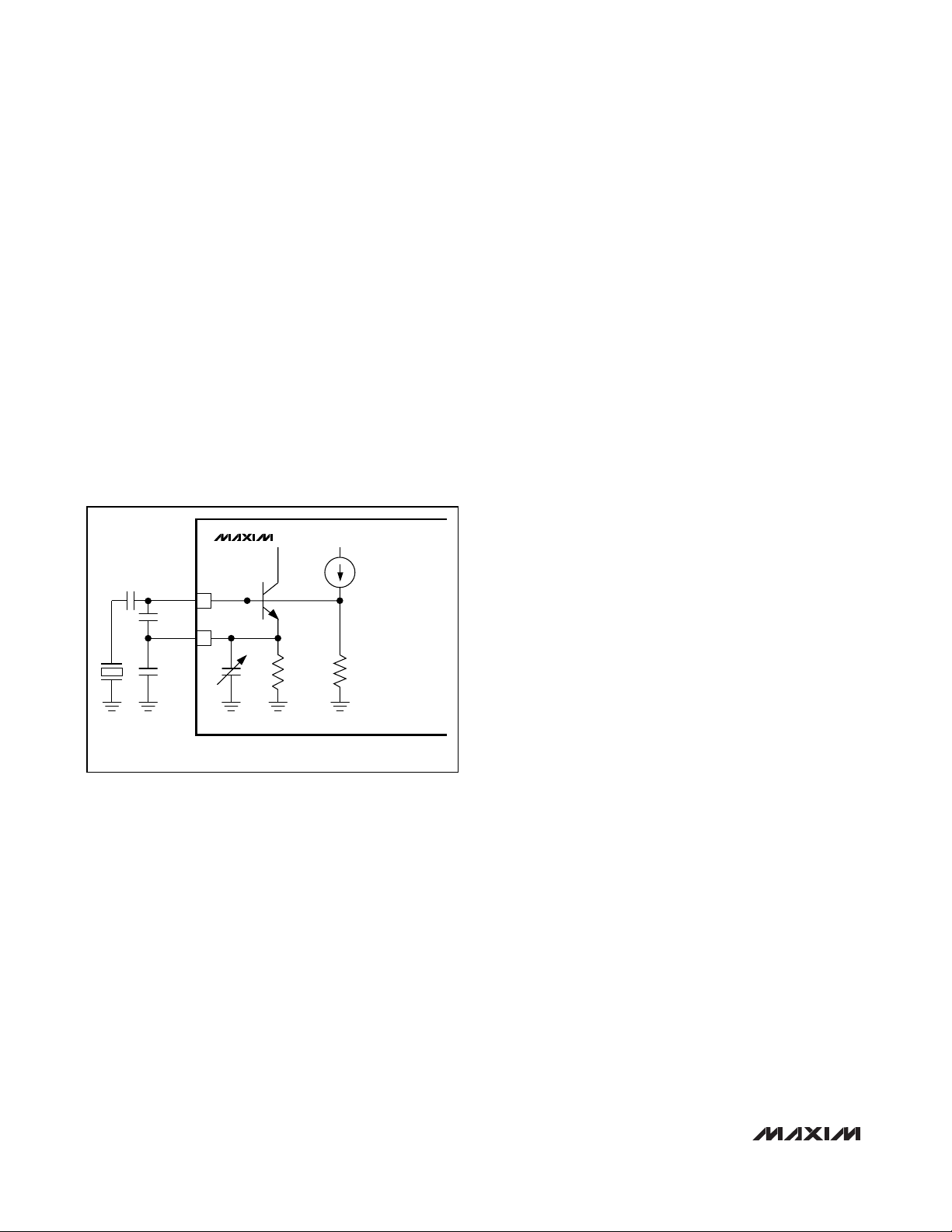
Crystal Oscillator
The crystal oscillator has been optimized to work with
low-cost crystals (e.g., Kyocera CX-3225SB). See Figure
1. The crystal oscillator frequency can be fine tuned
through bits D6:D0 in Register 14 (A3:A0 = 1110), which
control the value of C
TUNE
from 0.5pF to 15.4pF in
0.12pF steps. See the Crystal-Oscillator Offset
Frequency vs. Crystal-Oscillator Tuning Bits graph in the
Typical Operating Characteristics. The crystal oscillator
can be used as a buffer for an external reference frequency source. In this case, the reference signal is ACcoupled to the XTAL pin, and capacitors C1 and C2 are
not connected. When used as a buffer, the XTAL input
pin has to be AC-coupled. The XTAL pin has an input
impedance of 5kΩ || 4pF, (set D6:D0 = 0000000 in
Register 14 A3:A0 = 1110).
Reference Clock Output Divider/Buffer
The reference oscillator of the MAX2831/MAX2832 has
a divider and a buffered output for routing the reference clock to the accompanying baseband IC. Bit D10
in Register 14 (A3:A0 = 1110) sets the buffer divider to
divide by 1 or 2, independent of the divide ratio for the
reference frequency provided to the PLL. Bit B9 in the
same register enables or disables the reference buffer
output. See the Clock Output waveform in the Typical
Operating Characteristics.
Loop Filter
The PLL charge-pump output, CPOUT (pin 24), connects to an external third-order, lowpass RC loop-filter,
which in turn connects to the voltage tuning input,
TUNE (pin 32), of the VCO, completing the PLL loop.
The charge-pump output sink and source current is
1mA, and the VCO tuning gain is 103MHz/V at 0.5V
tune voltage and 86MHz/V at 2.2V tune voltage. The RC
loop-filter values have been optimized for a loop bandwidth of 150kHz, to achieve the desired Tx/Rx turnaround settling time, while maintaining loop stability
and good phase noise. Refer to the MAX2831 EV kit
schematic for the recommended loop-filter component
values. Keep the line from this pinto the tune input as
short as possible to prevent spurious pickup.
Lock-Detector Output
The PLL features a logic lock-detect output. A logic-high
indicates the PLL is locked, and a logic-low indicates
the PLL is not locked. Bit D5 in Register 5 (A3:A0 =
0101) enables or disables the lock-detect output. Bit
D12 in Register 1 (A3:A0 = 0001) configures the lockdetect output as a CMOS or open-drain output. In opendrain output mode, bit D9 in Register 5 (A3:A0 = 0101)
enables or disables an internal 30kΩ pullup resistor
from the open-drain output.
Figure 1. Crystal Oscillator Schematic
MAX2831
MAX2832
XTAL
28
C1
CTUNE
29
C2
FOR EXTERNAL REFERENCE CLOCK SET, C1 = C2 = OPEN
C
1.35kΩ
TUNE
5.9kΩ
Page 27

MAX2831/MAX2832
2.4GHz to 2.5GHz 802.11g/b
RF Transceivers with Integrated PA
______________________________________________________________________________________ 27
*The power-on register settings are not production tested. Recommended register settings must be loaded after VCCis supplied.
Table 14. Recommended Register Settings*
Figure 2. 3-Wire SPI Serial-Interface Timing Diagram
Programmable Registers and
3-Wire SPI-Interface
The MAX2831/MAX2832 include 16 programmable, 18bit registers. The 14 most significant bits (MSBs) are
used for register data. The 4 least significant bits
(LSBs) of each register contain the register address.
See Table 14 for a summary of the registers and recommended register settings.
Register data is loaded through the 3-wire SPI/
MICROWIRE™-compatible serial interface. Data is
shifted in MSB first and is framed by CS. When CS is
low, the clock is active, and data is shifted with the rising edge of the clock. When CS transitions high, the
shift register is latched into the register selected by the
contents of the address bits. See Figure 2. Only the last
18 bits shifted into the device are retained in the shift
register. No check is made on the number of clock
pulses. For programming data words less than 14 bits
long, only the required data bits and the address bits
need to be shifted, resulting in faster Rx and Tx gain
control where only the LSBs need to be programmed.
MICROWIRE is a trademark of National Semiconductor Corp.
REGISTER
0 01011101000000 0000 15
1 01000110011010 0001 16
2 01000000000011 0010 17
3 00000001111001 0011 18
4 11011001100110 0100 19
5 00000010100100 0101 20
6 00000001100000 0110 21
7 01000000100010 0111 22
8 10000000100001 1000 23
9 00001110110101 1001 24
10 01110110100100 1010 25
11 00000001111111 1011 26
12 00000101000000 1100 27
13 00111010010010 1101 28
14 00001100111011 1110 29
15 00000101000101 1111 30
D13 D12 D11 D10 D9 D8 D7 D6 D5 D4 D3 D2 D1 D0 (A3:A0)
DATA ADDRESS
TABLE
DIN
SCLK
t
DS
CS
t
t
CSS
CSO
t
DH
BIT 16BIT 2BIT 1 BIT 24BIT 23BIT 15
t
t
CL
CH
t
CSH
t
CSW
t
CS1
Page 28

MAX2831/MAX2832
2.4GHz to 2.5GHz 802.11g/b
RF Transceivers with Integrated PA
28 ______________________________________________________________________________________
Table 20. Register 5 (A3:A0 = 0101)
Table 15. Register 0 (A3:A0 = 0000)
Table 16. Register 1 (A3:A0 = 0001)
Table 17. Register 2 (A3:A0 = 0010)
This register contains the 8-bit integer portion and 6 LSBs of the fractional portion of the divider ratio of the synthesizer.
Table 18. Register 3 (A3:A0 = 0011)
Table 19. Register 4 (A3:A0 = 0100)
DATA BITS RECOMMENDED DESCRIPTION
D13:D11 000 Set to recommended value.
D10 1
D9:D0 1101000000 Set to recommended value.
Fractional-N PLL Mode Enable. Set 1 to enable the fractional-N PLL or set 0 to enable the
integer-N PLL.
DATA BITS RECOMMENDED DESCRIPTION
D13 0 Set to recommended value.
Lock-Detector Output Select. Set to 1 for CMOS Output. Set to 0 for open-drain output. Bit D9
D12 1
D11:D0 000110011010 Set to recommended value.
in register (A3:A0 = 0101) enables or disables an internal 30kΩ pullup resistor in open-drain
output mode.
DATA BITS RECOMMENDED DESCRIPTION
D13:D0 01000000000011 Set to recommended value.
BIT RECOMMENDED DESCRIPTION
D13:D8 00000 6 LSBs of 20-Bit Fractional Portion of Main Divider
D7:D0 01111001 8-Bit Integer Portion of Main Divider. Programmable from 64 to 255.
BIT RECOMMENDED DESCRIPTION
D13:D0 11011001100110 14 MSBs of 20-Bit Fractional Portion of Main Divider
BIT RECOMMENDED DESCRIPTION
D13:D10 0000 Set to recommended value.
Lock-Detect Output Internal Pullup Resistor Enable. Set to 1 to enable internal 30kΩ pullup
D9 0
D8:D6 010 Set to recommended value.
D5 1
D4:D3 00 Set to recommended value.
D2 1 Reference Frequency Divider Ratio to PLL. Set to 0 to divide by 1. Set to 1 to divide by 2.
D1:D0 00 Set to recommended value.
resistor or set to 0 to disable the resistor. Only available when lock-detect, open-drain output
is selected (A3:A0 = 0010, D12 = 1).
Lock-Detect Output Enable. Set to 1 to enable the lock-detect output or set to 0 to disable the
output. The output is high impedance when disabled.
Page 29

MAX2831/MAX2832
2.4GHz to 2.5GHz 802.11g/b
RF Transceivers with Integrated PA
______________________________________________________________________________________ 29
Table 21. Register 6 (A3:A0 = 0110)
Table 22. Register 7 (A3:A0 = 0111)
Table 23. Register 8 (A3:A0 = 1000)
DATA BIT RECOMMENDED DESCRIPTION
D13 0 Set to recommended value.
D12:D11 00
D10:D7 0000 Set to recommended value.
D6 1
D5:D2 1000 Set to recommended value.
D1 0
D0 0
Tx I/Q Calibration LO Leakage and Sideband Detector Gain-Control Bits. D12:D11 = 00: 9dB;
01 19dB; 10: 29dB; 11: 39dB.
Power-Detector Enable in Tx Mode. Set to 1 to enable the power detector or set to 0 to
disable the detector.
Tx Calibration Mode. Set to 1 to place the device in Tx calibration mode or 0 to place the
device in normal Tx mode when RXTX is set to 1 (see Table 31).
Rx Calibration Mode. Set to 1 to place the device in Rx calibration mode or 0 to place the
device in normal Rx mode when RXTX is set to 0 (see Table 31).
BIT RECOMMENDED DESCRIPTION
D13:D12 01
D11:D6 000000 Set to recommended value.
D5:D3 100
D2:D0 010
Receiver Highpass Corner Frequency Setting for RXHP = 0. Set to 00 for 100Hz, X1 for 4kHz,
and 10 for 30kHz.
Transmitter Lowpass Filter Corner Frequency Fine Adjustment (Relative to Coarse Setting).
See Table 8. Bits D1:D0 in A3:A0 = 1000 provide the lowpass filter corner coarse adjustment.
Receiver Lowpass Filter Corner Frequency Fine Adjustment (Relative to Coarse Setting). See
Table 5. Bits D1:D0 in A3:A0 = 1000 provide the lowpass filter corner coarse adjustment.
BIT RECOMMENDED DESCRIPTION
D13 1 Set to recommended value.
Enable Receiver Gain Programming Through the Serial Interface. Set to 1 to enable
D12 0
D11 0 Set to recommended value.
D10 0
D9:D8 00
D7:D2 001000 Set to recommended value.
D1:D0 01
programming through the 3-wire serial interface (D6:D0 in Register A3:A0 = 1011). Set to 0 to
enable programming in parallel through external digital pins (B7:B1).
RSSI Operating Mode. Set to 1 to enable RSSI output independent of RXHP. Set to 0 to
disable RSSI output if RXHP = 0, and enable the RSSI output if RXHP = 1.
RS S I, P ow er D etector or Tem p er atur e S ensor O utp ut S el ect. S et to 00 to enab l e the RS S I
outp ut i n r ecei ve m od e. S et to 01 to enab l e the tem p er atur e sensor outp ut i n r ecei ve and
tr ansm i t m od es. S et to 10 to enab l e the p ow er - d etector outp ut i n tr ansm i t m od e. S ee Tab l e 7.
Receiver and Transmitter Lowpass Filter Corner Frequency Coarse Adjustment. See Tables 4
and 7.
Page 30
MAX2831/MAX2832
2.4GHz to 2.5GHz 802.11g/b
RF Transceivers with Integrated PA
30 ______________________________________________________________________________________
Table 26. Register 11 (A3:A0 = 1011)
Table 27. Register 12 (A3:A0 = 1100)
Table 28. Register 13 (A3:A0 = 1101)
Table 25. Register 10 (A3:A0 = 1010)
Table 24. Register 9 (A3:A0 = 1001)
BIT RECOMMENDED DESCRIPTION
D13:D11 000 Set to recommended value.
Enable Transmitter Gain Programming Through the Serial or Parallel Interface. Set to 1 to
D10 0
D9:D0 1110110101 Set to recommended value.
BIT RECOMMENDED DESCRIPTION
D13:D10 0111
D9:D7 011 Set to recommended value.
D6:D3 0100 Second-Stage Power-Amplifier Bias Current Adjustment. Set to XXXX for 802.11g/b.
D2:D0 100 First-Stage Power-Amplifier Bias Current Adjustment. Set to XXX for 802.11g/b.
enable programming through the 3-wire serial interface (D5:D0 in Register A3:A0 = 1011).
Set to 0 to enable programming in parallel through external digital pins (B6:B1).
P ow er - Am p l i fi er E nab l e D el ay. S ets a d el ay b etw een RX TX l ow - to- hi g h tr ansi ti on and i nter nal P A
enab l e. P r og r am m ab l e i n 0.5µs step s. D 13:D 10 = 0001 ( 0.2µs) and D 13:D 10 = 1111 ( 7µs) .
BIT RECOMMENDED DESCRIPTION
D13:D7 0000000 Set to recommended value.
D6:D5 11
D4:D0 11111
LNA Gain Control. Set to 11 for high-gain mode. Set to 10 for medium-gain mode, reducing
LNA gain by 16dB. Set to 0X for low-gain mode, reducing LNA gain by 33dB.
Receiver VGA Control. Set D4:D0 = 00000 for minimum gain and D4:D0 = 11111 for
maximum gain.
BIT RECOMMENDED DESCRIPTION
D13:D6 00000101 Set to recommended value.
D5:D0 000000
Transmitter VGA Gain Control. Set D5:D0 = 000000 for minimum gain, and set D5:D0 =
111111 for maximum gain.
BIT RECOMMENDED DESCRIPTION
D13:D10 0011 Set to recommended value.
D9:D6 1010 Set to recommended value.
D5:D0 010010 Set to recommended value.
Page 31

MAX2831/MAX2832
2.4GHz to 2.5GHz 802.11g/b
RF Transceivers with Integrated PA
______________________________________________________________________________________ 31
Table 29. Register 14 (A3:A0 = 1110)
Table 30. Register 15 (A3:A0 = 1111)
Table 31. Operating Mode Table
X = Don’t care.
X = Don’t care.
BIT RECOMMENDED DESCRIPTION
D13:D11 000 Set to recommended value.
D10 0 Reference Clock Output Divider Ratio. Set 1 to divide by 2 or set 0 to divide by 1.
D9 1 Refer ence C l ock Outp ut E nab l e. S et 1 to enab l e the r efer ence cl ock outp ut or set 0 to d i sab l e.
D8:D7 10 Set to recommended value.
D6:D0 XXXXXXX Crystal-Oscillator Fine Tune. Tunes crystal oscillator over ±20ppm to within ±1ppm.
BIT RECOMMENDED DESCRIPTION
D13:D12 00 Set to recommended value.
D11:D10 00
D9:D0 0101000101 Set to recommended value.
Receiver I/Q Output Common-Mode Voltage Adjustment. Set D11:D10 = 00: 1.1V,
01: 1.2V, 10: 1.3V, 11: 1.45V.
LOGIC PINS
MODE
SHDN RXTX
Shutdown 0 0 00 Off Off Off None
Standby 0 1 00 Off Off On None
Rx 1 0 X0 On Off On None
Tx 1 1 0X Off On On None
Rx Calibration 1 0 X1
Tx Calibration 1 1 1X Off
REGISTER
SETTINGS
D1:D0
(A3:A0 = 0110)
Rx PATH Tx PATH
On
(except LNA)
CIRCUIT BLOCK STATES
PLL, VCO,
LO GEN,
AUTO-TUNER
Upconverters On
On (except PA
driver and PA)
C al tone, RF p hase
On
CALIBRATION
SECTIONS ON
shi ft, Tx fi l ter
AM detector,
Rx I/Q buffers
Page 32

MAX2831/MAX2832
2.4GHz to 2.5GHz 802.11g/b
RF Transceivers with Integrated PA
32 ______________________________________________________________________________________
Modes of Operation
The modes of operation for the MAX2831/MAX2832 are
shutdown, standby, transmit, receive, transmitter calibration, and receiver calibration. See Table 31 for a summary of the modes of operation. The logic-input pins, SHDN
(pin 12) and RXTX (pin 48), control the various modes.
Shutdown Mode
The MAX2831/MAX2832 feature a low-power shutdown
mode that disables all circuit blocks, except the serialinterface and internal registers, allowing the registers to
be loaded and values maintained, as long as V
CC
is
applied. Set SHDN and RXTX logic-low to place the
device in shutdown mode.
After supply voltage ramp up, supply current in shutdown mode could be high. Program the default value to
SPI register 0 to eliminate high shutdown current.
Standby Mode
The standby mode is used to enable the frequency
synthesizer block while the rest of the device is powered down. In this mode, the PLL, VCO, and LO generators are on, so that Tx or Rx modes can be quickly
enabled from this mode. Set SHDN to a logic-low and
RXTX to a logic-high to place the device in standby
mode.
Receive (Rx) Mode
The complete receive signal path is enabled in this
mode. Set SHDN to logic-high and RXTX to logic-low to
place the device in Rx mode.
Transmit (Tx) Mode
The complete transmitter signal path is enabled in this
mode. Set SHDN and RXTX to logic-high to place the
device in Tx mode.
Tx/Rx Calibration Mode
The MAX2831/MAX2832 feature Rx/Tx calibration modes
to detect I/Q imbalances and transmit LO leakage. In the
Tx calibration mode, all Tx circuit blocks, except the PA
driver and external PA, are powered on and active. The
AM detector and receiver I and Q channel buffers are
also on, along with multiplexers in the receiver side to
route this AM detector’s signal. In this mode, the LO
leakage calibration is done only for the LO leakage signal that is present at the center frequency of the channel
(i.e., in the middle of the OFDM or QPSK spectrum). The
LO leakage calibration includes the effect of all DC offsets in the entire baseband paths of the I/Q modulator
and direct leakage of the LO to the I/Q modulator output.
The LO leakage and sideband detector output are
taken at the receiver I and Q channel outputs during
this calibration phase.
During Tx LO leakage and I/Q imbalance calibration, a
sine and cosine signal (f = f
TONE
) is input to the baseband I/Q Tx pins from the baseband IC. At the LO leakage and sideband-detector output, the LO leakage
corresponds to the signal at f
TONE
and the sideband
suppression corresponds to the signal at 2 x f
TONE
. The
output power of these signals vary 1dB for 1dB of variation in the LO leakage and sideband suppression. To
calibrate the Tx path, first set the power-detector gain
to 9dB using D12:D11 in Register 5 (see Table 21).
Adjust the DC offset of the baseband inputs to minimize
the signal at f
TONE
(LO leakage). Then, adjust the baseband input relative magnitude and phase offsets to
reduce the signal at 2 x f
TONE
.
In Rx calibration mode, the calibrated Tx RF signal is
internally routed to the Rx inputs. In this mode, the
VCO/LO generator/PLL blocks are powered on and
active except for the low-noise amplifier (LNA).
Applications Information
Layout Issues
The MAX2831 EV kit can be used as a starting point for
layout. For best performance, take into consideration
grounding and RF, baseband, and power-supply routing. Make connections from vias to the ground plane as
short as possible. Do not connect the device ground
pin to the exposed paddle ground. Keep the buffered
clock output trace as short as
possible. Do not share the trace with the RF input layer,
especially on or inter-layer or back side of the board.
On the high-impedance ports, keep traces short to minimize shunt capacitance. EV kit Gerber files can be
requested at www.maxim-ic.com.
Power-Supply Layout
To minimize coupling between different sections of the
IC, a star power-supply routing configuration with a
large decoupling capacitor at a central VCCnode is recommended. The VCCtraces branch out from this node,
each going to a separate VCCnode in the circuit. Place
a bypass capacitor as close as possible to each supply
pin. This arrangement provides local decoupling at
each V
CC
pin. Use at least one via per bypass capacitor
for a low-inductance ground connection. Do not share
the capacitor ground vias with any other branch and the
exposed paddle ground.
Page 33

MAX2831/MAX2832
2.4GHz to 2.5GHz 802.11g/b
RF Transceivers with Integrated PA
______________________________________________________________________________________ 33
POWER
Figure 3. Timing Diagram
Pin Configuration
Chip Information
PROCESS: BiCMOS
Package Information
For the latest package outline information and land patterns
(footprints), go to www.maxim-ic.com/packages
. Note that a
"+", "#", or "-" in the package code indicates RoHS status only.
Package drawings may show a different suffix character, but
the drawing pertains to the package regardless of RoHS status.
POWER SUPPLY
ON
I
REF
3-WIRE SERIAL INTERFACE AVAILABLE
SHDN
MAC
RXTX
CS
SCLK
MAC SPI
DIN
TOP VIEW
V
CCLNA
GNDRXLNA
RXRF+
RXRF-
V
CCPA
TXRF+
TXRF-
SHDN
B6
B7
B3
10
B2
11
12
GNDTEST
RXTX
48 47 46 45 44 43 42 41 40 39 38 37
+
1
2
3
4
5
6
7
8
9
13 14 15 16 17 18 19 20 21 22 23 24
B5
CS
CCTXPA
V
SHUTDOWN
CS (SELECT)
MAX2831/MAX2832
SCLK (CLOCK)
DIN (DATA)
INTERNAL PA
ENABLED
CCRXMX
V
TXBBI+
RSSI
TXBBQ+
TXBBI-
MAX2831
MAX2832
SCLK
CCTXMX
V
TQFN
TXBBQ-
DIN
SPI:
CHANNEL FREQUENCY, PA BIAS, TRANSMITTER LINEARITY,
RECEIVER RSSI OPERATION, CALIBRATION MODE, ETC.
(DRIVES POWER RAMP CONTROL)
SHUTDOWN
MODE
CCRXVGA
CCRXFL
V
CCPLL
V
RXHP
CLOCKOUT
RXBBI-
RXBBI+
V
EP
B1
LD
CPOUT
36
35
34
33
32
31
30
29
28
27
26
25
RXBBQ+
RXBBQ-
B4
BYPASS
TUNE
GNDVCO
V
CCVCO
CTUNE
XTAL
V
CCXTAL
GNDCP
V
CCCP
STANDBY
MODE
0 TO 7µs
RECEIVE
MODE
PA ENABLE
TRANSMIT
MODE
PACKAGE
TYPE
48 TQFN- E P T4877+ 4
PACKAGE
CODE
OUTLINE
NO.
21 - 01 44
LAND PATTERN
NO.
90 - 01 30
Page 34

MAX2831/MAX2832
2.4GHz to 2.5GHz 802.11g/b
RF Transceivers with Integrated PA
Maxim cannot assume responsibility for use of any circuitry other than circuitry entirely embodied in a Maxim product. No circuit patent licenses are
implied. Maxim reserves the right to change the circuitry and specifications without notice at any time.
34 ____________________Maxim Integrated Products, 120 San Gabriel Drive, Sunnyvale, CA 94086 408-737-7600
© 2011 Maxim Integrated Products Maxim is a registered trademark of Maxim Integrated Products, Inc.
Revision History
REVISION
NUMBER
0 10/06 Initi al rel ease —
1 3/10 Removed MAX2832 future product reference and made minor corrections 1, 2, 10, 18, 19, 20
23/11
REVISION
DATE
DESCRIPTION
Corrected conditions for Rx I/Q Output Common-Mode Voltage Variation in the
DC Electrical Characteristics; corrected Tables 14, 17, and 27; added text to
Shutdown Mode section
PAGES
CHANGED
2, 27, 28,
30, 32
 Loading...