

Page 1
General Description
The MAX2828/MAX2829 single-chip, RF transceiver ICs
are designed specifically for OFDM 802.11 WLAN applications. The MAX2828 is designed for single-band
802.11a applications covering world-band frequencies
of 4.9GHz to 5.875GHz. The MAX2829 is designed for
dual-band 802.11a/g applications covering world-bands
of 2.4GHz to 2.5GHz and 4.9GHz to 5.875GHz. The ICs
include all circuitry required to implement the RF transceiver function, providing a fully integrated receive path,
transmit path, VCO, frequency synthesizer, and baseband/control interface. Only the PA, RF switches, RF
bandpass filters (BPF), RF baluns, and a small number
of passive components are needed to form the complete RF front-end solution.
Each IC completely eliminates the need for external SAW
filters by implementing on-chip monolithic filters for both
the receiver and transmitter. The baseband filtering and
the Rx/Tx signal paths are optimized to meet the
802.11a/g IEEE standards and cover the full range of the
required data rates (6, 9, 12, 18, 24, 36, 48, and 54Mbps
for OFDM; 1, 2, 5.5, and 11Mbps for CCK/DSSS), at
receiver sensitivity levels up to 10dB better than 802.11a/g
standards. The MAX2828/MAX2829 transceivers are available in the small 56-pin, exposed paddle thin QFN package.
Applications
Single-/Dual-Band 802.11a/b/g Radios
4.9GHz Public Safety Radios
2.4GHz/5GHz MIMO and Smart Antenna Systems
Features
♦ World-Band Operation
MAX2828: 4.9GHz to 5.875GHz (802.11a)
MAX2829: 2.4GHz to 2.5GHz and 4.9GHz to
5.875GHz (802.11a/b/g)
♦ Best-In-Class Transceiver Performance
-75dBm Rx Sensitivity at 54Mbps (802.11g)
-46dB (802.11g)/-51dB (802.11a) Tx Sideband
Suppression
1.5% (802.11g) and 2% (802.11a) Tx EVM
-100dBc/Hz (802.11g)/-95dBc/Hz (802.11a)
LO Phase Noise
Programmable Baseband Lowpass Filters
Integrated PLL with 3-Wire Serial Interface
93dB (802.11g)/97dB (802.11a) Receiver Gain-
Control Range
200ns Rx I/Q DC Settling
60dB Dynamic Range Rx RSSI
30dB Tx Power-Control Range
Tx/Rx I/Q Error Detection
I/Q Analog Baseband Interface for Tx and Rx
Digital Mode Selection (Tx, Rx, Standby, and
Power Down)
Supports Both Serial and Parallel Gain Control
♦ MIMO and Smart Antenna Compatibility
Coherent LO Phase Among Multiple
Transceivers
♦ Support 40MHz Channel Bandwidth (Turbo Mode)
♦ Single +2.7V to +3.6V Supply
♦ 1µA Low-Power Shutdown Mode
♦ Small 56-Pin TQFN Package (8mm x 8mm)
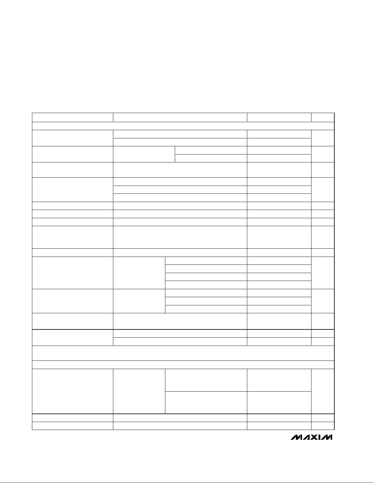
MAX2828/MAX2829
Single-/Dual-Band 802.11a/b/g
World-Band Transceiver ICs
________________________________________________________________ Maxim Integrated Products 1
2
1
3
4
5
6
7
8
B6
TOP VIEW
V
CC
V
CC
B7
N.C.
N.C.
N.C.
GND
RXRFH
GND
TXRFH+
B2
GND
B4
V
CC
V
CC
VCCV
CC
B5
B3
9
TXRFH-
TXENA
PABIAS
V
CC
VCCV
CC
V
CC
TXBBI+
TXBBI-
TXBBQ+
TXBBQ-
R
BIAS
V
REF
GND
DIN
SCLK
RXENA
RXHP
RSSI
V
CC
V
CC
BYPASS
GND
GND
CPOUT
GND
ROSC
LD
B1
RXBBI+
RXBBI-
RXBBQ+
RXBBQ-
10
11
12
13
15 16 17 18 19 201421 22 23 24 25 26 27 28
29
33
32
31
34
35
36
37
38
39
40
41
42
55 54 53 52 51 50 49 48 47 46 45 44 4356
30
TUNE
CS
MAX2828
SHDN
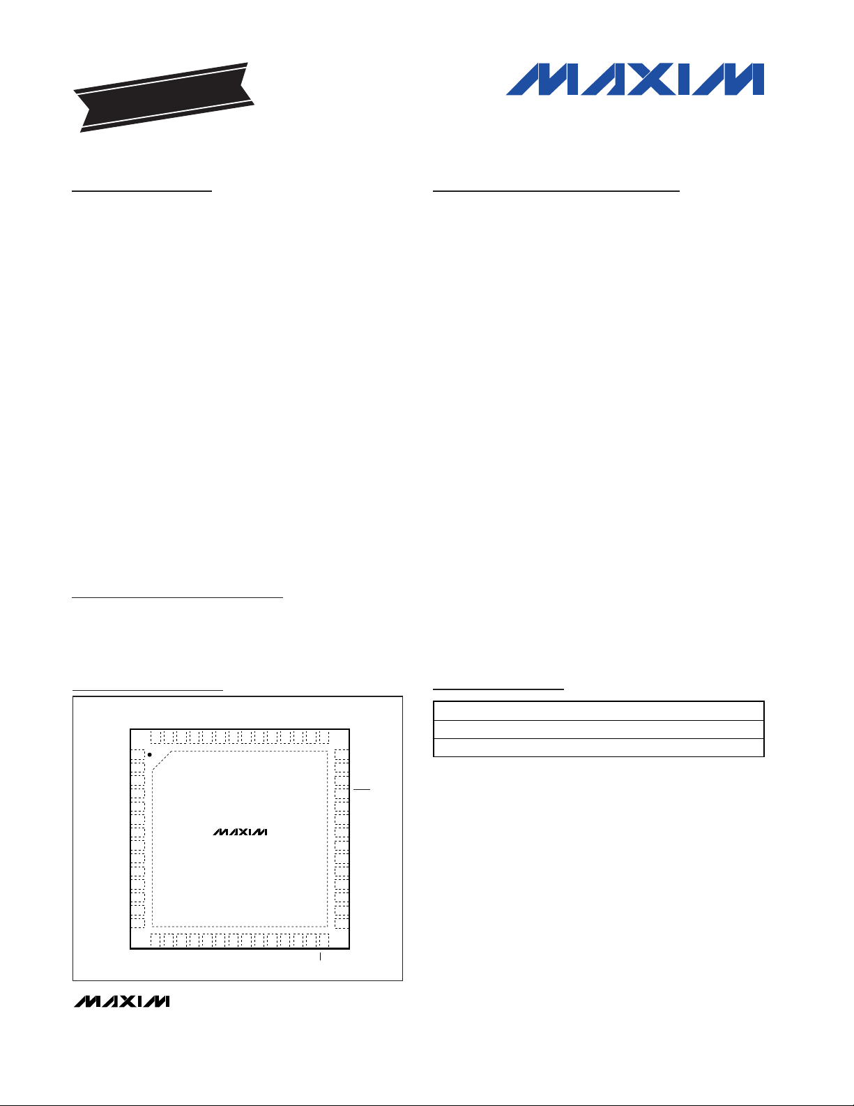
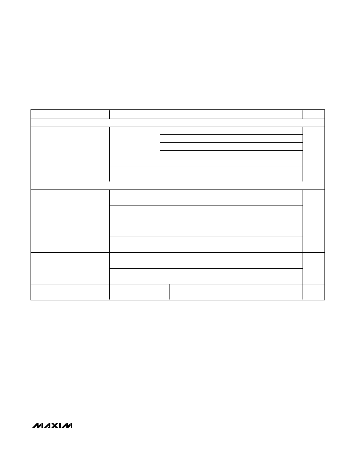
Pin Configurations
Ordering Information
19-3455; Rev 0; 10/04
For pricing, delivery, and ordering information, please contact Maxim/Dallas Direct! at
1-888-629-4642, or visit Maxim’s website at www.maxim-ic.com.
*EP = Exposed paddle.
EVALUATION KIT
AVAILABLE
PART
TEMP RANGE
PIN-PACKAGE
MAX2828 ETN
56 TQFN-EP* (T5688-2)
MAX2829 ETN
56 TQFN-EP* (T5688-2)
Pin Configurations continued at end of data sheet.
-40°C to +85°C
-40°C to +85°C
Page 2
MAX2828/MAX2829
Single-/Dual-Band 802.11a/b/g
World-Band Transceiver ICs
2 _______________________________________________________________________________________
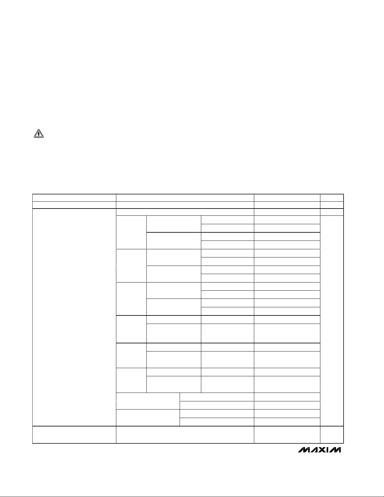
ABSOLUTE MAXIMUM RATINGS
Stresses beyond those listed under “Absolute Maximum Ratings” may cause permanent damage to the device. These are stress ratings only, and functional
operation of the device at these or any other conditions beyond those indicated in the operational sections of the specifications is not implied. Exposure to
absolute maximum rating conditions for extended periods may affect device reliability.
VCC, TXRFH_, TXRFL_ to GND..............................-0.3V to +4.2V
RXRFH, RXRFL, TXBBI_, TXBBQ_, ROSC, RXBBI_, RXBBQ_,
RSSI, PABIAS, V
REF
, CPOUT, RXENA, TXENA, SHDN, CS,
SCLK, DIN, B_, RXHP, LD, R
BIAS
,
BYPASS to GND....................................-0.3V to (V
CC
+ 0.3V)
RXBBI_, RXBBQ_, RSSI, PABIAS, V
REF
, CPOUT,
LD Short-Circuit Duration...................................................10s
RF Input Power ...............................................................+10dBm
Continuous Power Dissipation (T
A
= +70°C)
56-Pin Thin QFN (derate 31.3mW/°C above +70°C)....2500mW
Operating Temperature Range ...........................-40°C to +85°C
Junction Temperature......................................................+150°C
Storage Temperature Range .............................-65°C to +160°C
Lead Temperature (soldering, 10s) .................................+300°C
DC ELECTRICAL CHARACTERISTICS
(MAX2828/MAX2829 evaluation kits: VCC= 2.7V to 3.6V, Rx/Tx set to maximum gain, R
BIAS
= 11kΩ, no signal at RF inputs, all RF
inputs and outputs terminated into 50Ω, receiver baseband outputs are open, no signal applied to Tx I/Q BB inputs in Tx mode,
f
REFOSC
= 40MHz, registers set to default settings and corresponding test mode, TA= -40°C to +85°C, unless otherwise noted.
Typical values are at V
CC
= +2.7V and TA= +25°C, unless otherwise noted.) (Note 1)
PARAMETERS CONDITIONS
UNITS
Supply Voltage 2.7 3.6 V
1 100 µA
TA = +25°C3747
802.11g MAX2829
51
TA = +25°C4451
Standby
mode
802.11a
55
TA = +25°C
151
802.11g MAX2829
158
TA = +25°C
180
Rx mode
802.11a
188
TA = +25°C
164
802.11g MAX2829
175
TA = +25°C
184
Tx mode
802.11a
197
802.11g MAX2829 TA = +25°C65
Standby
mode
(MIMO)
(Note 2)
802.11a
TA = +25°C70
802.11g MAX2829 TA = +25°C
Rx mode
(MIMO)
(Note 2)
802.11a
TA = +25°C
802.11g MAX2829 TA = +25°C
Tx mode
(MIMO)
(Note 2)
802.11a
TA = +25°C
802.11g MAX2829
Tx calibration mode,
T
A
= +25°C
802.11g MAX2829
Supply Current
RX calibration mode,
TA = +25°C
mA
Rx I/Q Output Common-Mode
Voltage
T
A
= +25°C
0.9
V
CAUTION! ESD SENSITIVE DEVICE
Shutdown mode, reference oscillator not applied, VIL = 0
TA = -40°C to +85°C
MAX2828/MAX2829
MAX2828/MAX2829
MAX2828/MAX2829
MAX2828/MAX2829
MAX2828/MAX2829
MAX2828/MAX2829
802.11a MAX2828/MAX2829 147
802.11a MAX2828/MAX2829 210
T
TA = -40°C to +85°C
T
TA = -40°C to +85°C
T
= -40°C to +85°C
A
= -40°C to +85°C
A
= -40°C to +85°C
A
MIN TYP MAX
118
0.80
135
124
142
136
154
139
157
129
188
1.05
Page 3
MAX2828/MAX2829
Single-/Dual-Band 802.11a/b/g
World-Band Transceiver ICs
_______________________________________________________________________________________ 3
AC ELECTRICAL CHARACTERISTICS—802.11g Rx Mode (MAX2829)
(MAX2829 evaluation kit: VCC= +2.7V, fIN= 2.437GHz; receiver baseband I/Q outputs at 112mV
RMS
(-19dBV), f
REFOSC
= 40MHz,
SHDN = RXENA = CS = high, RXHP = TXENA = SCLK = DIN = low, R
BIAS
= 11kΩ, registers set to default settings and correspond-
ing test mode, T
A
= +25°C, unless otherwise noted. Unmodulated single-tone RF input signal is used, unless otherwise indicated.)
(Tables 1, 2, 3)
PARAMETER CONDITIONS
MIN
TYP
MAX
UNITS
RECEIVER SECTION: LNA RF INPUT TO BASEBAND I/Q OUTPUTS
RF Input Frequency Range
GHz
-22
LNA medium-gain mode
(B7:B6 = 10)
-24
RF Input Return Loss
With 50Ω external
match
-12
dB
TA = +25°C8794
Maximum gain,
B7:B1 = 1111111
T
A
= -40°C to +85°C (Note 1) 85
Total Voltage Gain
Minimum gain,
B7:B1 = 0000000
T
A
= +25°C1
dB
From high-gain mode (B7:B6 = 11) to medium-gain
mode (B7:B6 = 10) (Note 3)
-15.5
RF Gain Steps
From high-gain mode (B7:B6 = 11) to low-gain mode
(B7:B6 = 0X) (Note 3)
-30.5
dB
Gain Variation Over RF Band fRF = 2.412GHz to 2.5GHz 3 dB
Baseband Gain Range
From maximum baseband gain (B5:B1 = 11111) to
minimum baseband gain (B5:B1 = 00000)
62 dB
DC ELECTRICAL CHARACTERISTICS (continued)
(MAX2828/MAX2829 evaluation kits: VCC= 2.7V to 3.6V, Rx/Tx set to maximum gain, R
BIAS
= 11kΩ, no signal at RF inputs, all RF
inputs and outputs terminated into 50Ω, receiver baseband outputs are open, no signal applied to Tx I/Q BB inputs in Tx mode,
f
REFOSC
= 40MHz, registers set to default settings and corresponding test mode, TA= -40°C to +85°C, unless otherwise noted.
Typical values are at V
CC
= +2.7V and TA= +25°C, unless otherwise noted.) (Note 1)
PARAMETERS CONDITIONS
MIN
TYP
MAX
UNITS
TA = -40°C (relative to +25°C) -25
Rx I/Q Output Common-Mode
Voltage Variation
T
A
= +85°C (relative to +25°C) 20
mV
Tx Baseband Input CommonMode Voltage Operating Range
0.9 1.3 V
Tx Baseband Input Bias Current 13 µA
Reference Voltage Output -1mA < I
OUT
< +1mA 1.2 V
Digital Input-Voltage High, V
IH
VCC -
0.4
V
Digital Input-Voltage Low, V
IL
0.4 V
Digital Input-Current High, I
IH
-1 +1 µA
Digital Input-Current Low, I
IL
-1 +1 µA
LD Output-Voltage High, V
OH
Sourcing 100µA
V
CC
-
0.4
V
LD Output-Voltage Low, V
OL
Sinking 100µA 0.4 V
2.412 2.500
LNA high-gain mode (B7:B6 = 11)
LNA low-gain mode (B7:B6 = 0X)
5.5
Page 4
MAX2828/MAX2829
Single-/Dual-Band 802.11a/b/g
World-Band Transceiver ICs
4 _______________________________________________________________________________________
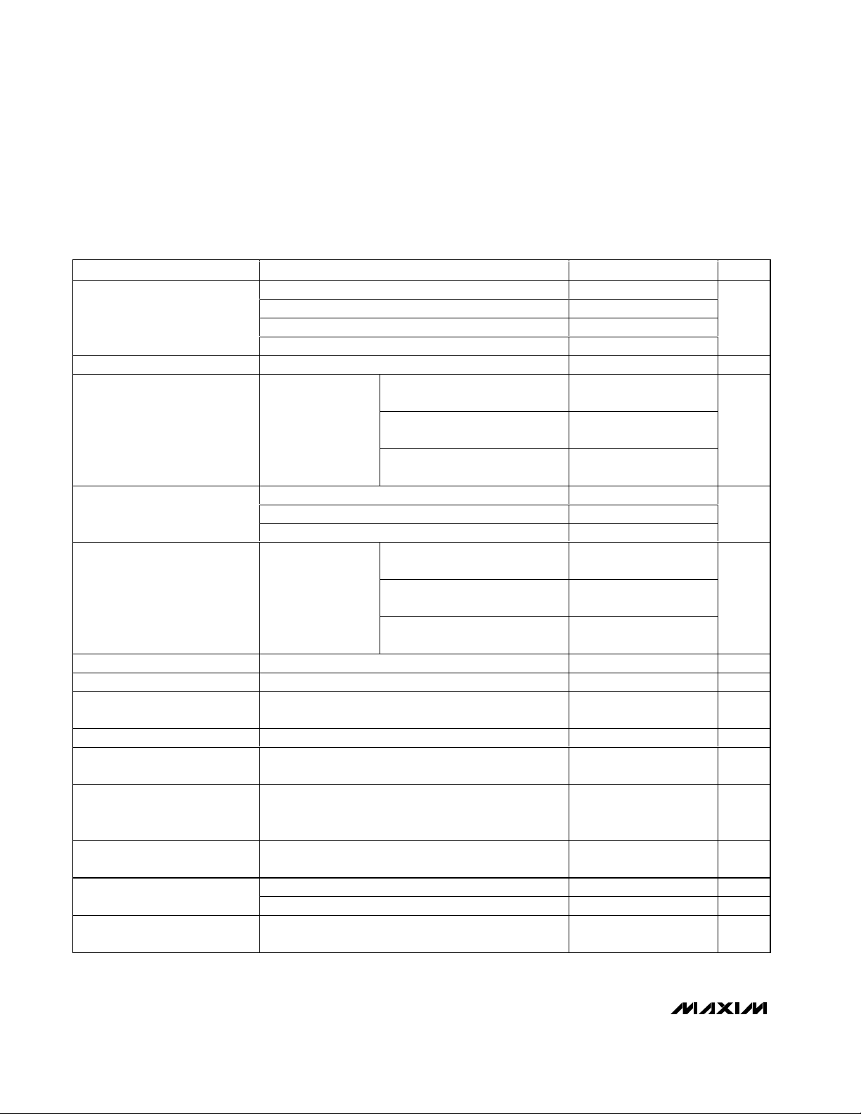
AC ELECTRICAL CHARACTERISTICS—802.11g Rx Mode (MAX2829) (continued)
(MAX2829 evaluation kit: VCC= +2.7V, fIN= 2.437GHz; receiver baseband I/Q outputs at 112mV
RMS
(-19dBV), f
REFOSC
= 40MHz,
SHDN = RXENA = CS = high, RXHP = TXENA = SCLK = DIN = low, R
BIAS
= 11kΩ, registers set to default settings and correspond-
ing test mode, T
A
= +25°C, unless otherwise noted. Unmodulated single-tone RF input signal is used, unless otherwise indicated.)
(Tables 1, 2, 3)
PARAMETER CONDITIONS
TYP
UNITS
Voltage gain ≥ 65dB, with B7:B6 = 11 3.5
Voltage gain = 50dB, with B7:B6 = 11 4
Voltage gain = 45dB, with B7:B6 = 10 16
DSB Noise Figure
Voltage gain = 15dB, with B7:B6 = 0X 36
dB
Output P-1
dB
Voltage gain = 90dB, with B7:B6 = 11 3.2
V
P-P
Voltage gain = 60dB,
with B7:B6 = 11
-10
Voltage gain = 45dB,
with B7:B6 = 10
-2
Out-of-Band Input IP3
-35dBm jammers at
40MHz and 78MHz
offset; based on IM3
at 2MHz
Voltage gain = 40dB,
with B7:B6 = 0X
21
dBm
Voltage gain = 40dB, with B7:B6 = 11 -29
Voltage gain = 25dB, with B7:B6 = 10 -14In-Band Input P-1
dB
Voltage gain = 5dB, with B7:B6 = 0X 2
dBm
Voltage gain = 40dB,
with B7:B6 = 11
-17
Voltage gain = 25dB,
with B7:B6 = 10
-5
In-Band Input IP3
Tones at 7MHz and
8MHz, IM3 at 6MHz
and 9MHz, P
IN
=
-40dBm per tone
Voltage gain = 5dB,
with B7:B6 = 0X
14
dBm
I/Q Phase Error B7:B1 = 1101110, 1σ variation ±0.5
degrees
I/Q Gain Imbalance B7:B1 = 1101110, 1σ variation ±0.1 dB
Tx-to-Rx Conversion Gain for Rx
I/Q Calibration
B7:B1 = 0010101 (Note 4) -4 dB
I/Q Static DC Offset RXHP = 1, B7:B1 = 1101110, 1σ variation ±2mV
I/Q DC Droop
After switching RXHP to 0, D2 = 0 (see the RX
Control/RSSI Register Definition section)
±1
mV/ms
RF Gain-Change Settling Time
Gain change from high gain to medium gain, high gain to
low gain, or medium gain to low gain; gain settling to
within ±2dB of steady state
0.4 µs
Baseband VGA Settling Time
Gain change from B5:B1 = 10111 to B5:B1 = 00111;
gain settling to within ±2dB of steady state
0.1 µs
Minimum differential resistance 10 kΩ
Rx I/Q Output Load Impedance
Maximum differential capacitance 8 pF
Spurious Signal Emissions at LNA
Input
RF = 1GHz to 26.5GHz -67
dBm
MIN
MAX
Page 5
MAX2828/MAX2829
Single-/Dual-Band 802.11a/b/g
World-Band Transceiver ICs
_______________________________________________________________________________________ 5
AC ELECTRICAL CHARACTERISTICS—802.11g Rx Mode (MAX2829) (continued)
(MAX2829 evaluation kit: VCC= +2.7V, fIN= 2.437GHz; receiver baseband I/Q outputs at 112mV
RMS
(-19dBV), f
REFOSC
= 40MHz,
SHDN = RXENA = CS = high, RXHP = TXENA = SCLK = DIN = low, R
BIAS
= 11kΩ, registers set to default settings and correspond-
ing test mode, T
A
= +25°C, unless otherwise noted. Unmodulated single-tone RF input signal is used, unless otherwise indicated.)
(Tables 1, 2, 3)
PARAMETER CONDITIONS
TYP
UNITS
RECEIVER BASEBAND FILTERS
Narrowband mode 7.5
Nominal mode 9.5
Turbo mode 1 14
Baseband -3dB Corner
Frequency
(See the Lowpass
Filter Register
section)
Turbo mode 2 18
MHz
f
BASEBAND
= 15MHz 20
f
BASEBAND
= 20MHz 39
Baseband Filter Rejection
(Nominal Mode)
f
BASEBAND
> 40MHz 84
dB
RSSI
RXHP = 1, low range (D11 = 0, see the Rx Control/RSSI
Register Definition section)
0.5
RSSI Minimum Output Voltage
RXHP = 1, high range (D11 = 1, see the Rx Control/RSSI
Register Definition section)
0.52
V
RXHP = 1, low range (D11 = 0, see the Rx Control/RSSI
Register Definition section)
2
RSSI Maximum Output Voltage
RXHP = 1, high range (D11 = 1, see the Rx Control/RSSI
Register Definition section)
2.5
V
RXHP = 1, low range (D11 = 0, see the Rx Control/RSSI
Register Definition section)
22.5
RSSI Slope
RXHP = 1, high range (D11 = 1, see the Rx Control/RSSI
Register Definition section)
30
mV/dB
+40dB signal step 0.2
RSSI Output Settling Time
To within 3dB of steady
state
-40dB signal step 0.7
µs
MIN
MAX
Page 6
MAX2828/MAX2829
Single-/Dual-Band 802.11a/b/g
World-Band Transceiver ICs
6 _______________________________________________________________________________________
AC ELECTRICAL CHARACTERISTICS—802.11a Rx Mode (MAX2828/MAX2829)
(MAX2828/MAX2829 evaluation kits: VCC= +2.7V, fIN= 5.25GHz; receiver baseband I/Q outputs at 112mV
RMS
(-19dBV), f
REFOSC
=
40MHz, SHDN = RXENA = CS = high, RXHP = TXENA = SCLK = DIN = low, R
BIAS
= 11kΩ, registers set to default settings and cor-
responding test mode, T
A
= +25°C, unless otherwise noted. Unmodulated single-tone RF input signal is used, unless otherwise indi-
cated.) (Tables 1, 2, 3)
PARAMETER CONDITIONS
TYP
UNITS
RECEIVER SECTION: LNA RF INPUT TO BASEBAND I/Q OUTPUTS
802.11a low-band mode
RF Input Frequency Range
802.11a high-band mode
GHz
-15
LNA medium-gain mode
(B7:B6 = 10)
-11
RF Input Return Loss
With 50Ω external
match
-7
dB
TA = +25°C9197
Maximum gain,
B7:B1 = 1111111
T
A
= -40°C to +85°C (Note 1) 88
Total Voltage Gain
Minimum gain,
B7:B1 = 0000000
T
A
= +25°C03
dB
From high-gain mode (B7:B6 = 11) to medium-gain
mode (B7:B6 = 10) (Note 3)
-19
RF Gain Steps
From high-gain mode (B7:B6 = 11) to low-gain mode
(B7:B6 = 0X) (Note 3)
-34.5
dB
fRF = 4.9GHz -0.3
fRF = 5.35GHz 0.4
Gain Variation Relative to
5.25GHz
f
RF
= 5.875GHz -4
dB
Baseband Gain Range
From maximum baseband gain (B5:B1 = 11111) to
minimum baseband gain (B5:B1 = 00000)
62 dB
Voltage gain ≥ 65dB, with B7:B6 = 11 4.5
Voltage gain = 50dB, with B7:B6 = 11 4.8
Voltage gain = 45dB, with B7:B6 = 10 15
DSB Noise Figure
Voltage gain = 15dB, with B7:B6 = 0X 36
dB
Output P-1
dB
Voltage gain = 90dB, with B7:B6 = 11 3.2
V
P-P
Voltage gain = 60dB,
with B7:B6 = 11
-15
Voltage gain = 45dB,
with B7:B6 = 10
0.5
Out-of-Band Input IP3
-35dBm jammers at
40MHz and 78MHz
offset; based on IM3
at 2MHz
Voltage gain = 40dB,
with B7:B6 = 0X
20
dBm
Voltage gain = 35dB, with B7:B6 = 11 -32
Voltage gain = 20dB, with B7:B6 = 10 -12In-Band Input P-1
dB
Voltage gain = 5dB, with B7:B6 = 0X 3
dBm
LNA high-gain mode (B7:B6 = 11)
LNA low-gain mode (B7:B6 = 0X)
MIN
4.900 5.350
5.470 5.875
MAX
Page 7
MAX2828/MAX2829
Single-/Dual-Band 802.11a/b/g
World-Band Transceiver ICs
_______________________________________________________________________________________ 7
AC ELECTRICAL CHARACTERISTICS—802.11a Rx Mode (MAX2828/MAX2829) (continued)
(MAX2828/MAX2829 evaluation kits: VCC= +2.7V, fIN= 5.25GHz; receiver baseband I/Q outputs at 112mV
RMS
(-19dBV), f
REFOSC
=
40MHz, SHDN = RXENA = CS = high, RXHP = TXENA = SCLK = DIN = low, R
BIAS
= 11kΩ, registers set to default settings and cor-
responding test mode, T
A
= +25°C, unless otherwise noted. Unmodulated single-tone RF input signal is used, unless otherwise indi-
cated.) (Tables 1, 2, 3)
PARAMETER CONDITIONS
TYP
UNITS
Voltage gain = 35dB,
with B7:B6 = 11
-24
Voltage gain = 20dB,
with B7:B6 = 10
-5
In-Band Input IP3
Tones at 7MHz and
8MHz, IM3 at 6MHz
and 9MHz, P
IN
=
-40dBm per tone
Voltage gain = 5dB,
with B7:B6 = 0X
13
dBm
I/Q Phase Error B7:B1 = 1101110, 1σ variation ±0.4
degrees
I/Q Gain Imbalance B7:B1 = 1101110, 1σ variation ±0.1 dB
Tx-to-Rx Conversion Gain for Rx
I/Q Calibration
B7:B1 = 0001111 (Note 4) 0 dB
I/Q Static DC Offset RXHP = 1, B7:B1 = 1101110, 1σ variation ±2mV
I/Q DC Droop
After switching RXHP to 0, D2 = 0 (see the Rx
Control/RSSI Register Definition section)
±1
mV/ms
RF Gain-Change Settling Time
Gain change from high gain to medium gain, high gain to
low gain, or medium gain to low gain; gain settling to
within ±2dB of steady state
0.4 µs
Baseband VGA Settling Time
Gain change from B5:B1 = 10111 to B5:B1 = 00111;
gain settling to within ±2dB of steady state
0.1 µs
Minimum differential resistance 10 kΩ
Rx I/Q Output Load Impedance
Maximum differential capacitance 8 pF
Spurious Signal Emissions at LNA
input
RF = 1GHz to 26.5GHz -50
dBm
RECEIVER BASEBAND FILTERS
Narrow-band mode 7.5
Nominal mode 9.5
Turbo mode 1 14
Baseband -3dB Corner
Frequency
(See the Lowpass
Filter Register
Definition section)
Turbo mode 2 18
MHz
f
BASEBAND
= 15MHz 20
f
BASEBAND
= 20MHz 39
Baseband Filter Rejection
(Nominal Mode)
f
BASEBAND
> 40MHz 80
dB
MIN
MAX
Page 8

MAX2828/MAX2829
Single-/Dual-Band 802.11a/b/g
World-Band Transceiver ICs
8 _______________________________________________________________________________________
AC ELECTRICAL CHARACTERISTICS—802.11a Rx Mode (MAX2828/MAX2829) (continued)
(MAX2828/MAX2829 evaluation kits: VCC= +2.7V, fIN= 5.25GHz; receiver baseband I/Q outputs at 112mV
RMS
(-19dBV), f
REFOSC
=
40MHz, SHDN = RXENA = CS = high, RXHP = TXENA = SCLK = DIN = low, R
BIAS
= 11kΩ, registers set to default settings and cor-
responding test mode, T
A
= +25°C, unless otherwise noted. Unmodulated single-tone RF input signal is used, unless otherwise indi-
cated.) (Tables 1, 2, 3)
PARAMETER CONDITIONS
MIN
TYP
MAX
UNITS
RSSI
RXHP = 1, low range (D11 = 0, see the Rx Control/RSSI
Register Definition section)
0.5
RSSI Minimum Output Voltage
RXHP = 1, high range (D11 = 1, see the Rx Control/RSSI
Register Definition section)
0.52
V
RXHP = 1, low range (D11 = 0, see the Rx Control/RSSI
Register Definition section)
2
RSSI Maximum Output Voltage
RXHP = 1, high range (D11 = 1, see the Rx Control/RSSI
Register Definition section)
2.5
V
RXHP = 1, low range (D11 = 0, see the Rx Control/RSSI
Register Definition section)
22.5
RSSI Slope
RXHP = 1, high range (D11 = 1, see the Rx Control/RSSI
Register Definition section)
30
mV/dB
+40dB signal step 0.2
RSSI Output Settling Time
To within 3dB of steady
state
-40dB signal step 0.7
µs
AC ELECTRICAL CHARACTERISTICS—802.11g Tx Mode (MAX2829)
(MAX2829 evaluation kit: VCC= +2.7V, f
OUT
= 2.437GHz, f
REFOSC
= 40MHz, SHDN = TXENA = CS = high, RXENA = SCLK = DIN =
low, R
BIAS
= 11kΩ, 100mV
RMS
sine and cosine signal (or 100mV
RMS
, 54Mbps IEEE 802.11g I/Q signals wherever OFDM is men-
tioned) applied to baseband I/Q inputs of transmitter, registers set to default settings and corresponding test mode, T
A
= +25°C,
unless otherwise noted.) (Table 4)
PARAMETER CONDITIONS
MIN
TYP
MAX
UNITS
TRANSMIT SECTION: Tx BASEBAND I/Q INPUTS TO RF OUTPUTS
RF Output Frequency Range, f
RF
GHz
1.5% EVM
Output Power
54Mbps 802.11g OFDM
signal
B6:B1 = 111011
dBm
Output Power (CW)
V
IN
= 100mV
RMS
at 1MHz I/Q CW signal, B6:B1 =
111111
-2
dBm
Output Power Range B6:B1 = 111111 to B6:B1 = 000000 30 dB
Carrier Leakage Without DC offset cancellation
dBc
Unwanted Sideband Suppression
Uncalibrated
dBc
Tx Output ACP
Measured with 1MHz resolution bandwidth at 22MHz
offset from channel center (B6:B1 = 111011), OFDM
signal
dBm/
MHz
RF Output Return Loss With external 50Ω match
dB
2.412 2.500
-2.5
-4.5
-27
-46
-69
-14
Page 9
MAX2828/MAX2829
Single-/Dual-Band 802.11a/b/g
World-Band Transceiver ICs
_______________________________________________________________________________________ 9
AC ELECTRICAL CHARACTERISTICS—802.11g Tx Mode (MAX2829) (continued)
(MAX2829 evaluation kit: VCC= +2.7V, f
OUT
= 2.437GHz, f
REFOSC
= 40MHz, SHDN = TXENA = CS = high, RXENA = SCLK = DIN =
low, R
BIAS
= 11kΩ, 100mV
RMS
sine and cosine signal (or 100mV
RMS
, 54Mbps IEEE 802.11g I/Q signals wherever OFDM is men-
tioned) applied to baseband I/Q inputs of transmitter, registers set to default settings and corresponding test mode, T
A
= +25°C,
unless otherwise noted.) (Table 4)
PARAMETER CONDITIONS
UNITS
2/3 x f
RF
4/3 x f
RF
5/3 x f
RF
RF Spurious Signal Emissions
B6:B1 = 111011, OFDM
signal
8/3 x f
RF
dBm/
MHz
Nominal mode 12
Turbo mode 1 18
Baseband -3dB Corner
Frequency
(See the Lowpass Filter
Register Definition
section)
Turbo mode 2 24
MHz
Baseband Filter Rejection
At 30MHz, in nominal mode (see the Lowpass Filter
Register Definition section)
60 dB
Minimum differential resistance 60 kΩ
Tx Baseband Input Impedance
Maximum differential capacitance 0.7 pF
TRANSMITTER LO LEAKAGE AND I/Q CALIBRATION USING LO LEAKAGE AND SIDEBAND DETECTOR (SEE THE Tx/Rx
CALIBRATION MODE SECTION)
Tx BASEBAND I/Q INPUTS TO RECEIVER OUTPUTS
Output at 1 x f
TONE
(for LO leakage
= -29dBc), f
TONE
= 2MHz,
100mV
RMS
-3
LO Leakage and SidebandDetector Output
Calibration register,
D12:D11 = 11,
A3:A0 = 0110
Output at 2 x f
TONE
(for sideband
suppression = -40dBc), f
TONE
=
2MHz, 100mV
RMS
-13
dBV
RMS
Amplifier Gain Range D12:D11 = 00 to D12:D11 = 11, A3:A0 = 0110 26 dB
Lower -3dB Corner Frequency
1
MHz
MIN TYP MAX
-64
-61
-63
-52
Page 10
MAX2828/MAX2829
Single-/Dual-Band 802.11a/b/g
World-Band Transceiver ICs
10 ______________________________________________________________________________________
AC ELECTRICAL CHARACTERISTICS—802.11a Tx Mode (MAX2828/MAX2829)
(MAX2828/MAX2829 evaluation kits: VCC= +2.7V, f
OUT
= 5.25GHz, f
REFOSC
= 40MHz, SHDN = TXENA = CS = high, RXENA = SCLK
= DIN = low, R
BIAS
= 11kΩ, 100mV
RMS
sine and cosine signal (or 100mV
RMS
, 54Mbps IEEE 802.11a I/Q signals wherever OFDM is
mentioned) applied to baseband I/Q inputs of transmitter, registers set to default settings and corresponding test mode, T
A
= +25°C,
unless otherwise noted.) (Table 4)
PARAMETER CONDITIONS
TYP
UNITS
TRANSMIT SECTION: Tx BASEBAND I/Q INPUTS TO RF OUTPUTS
802.11a low-band mode
RF Output Frequency Range, f
RF
802.11a high-band mode
GHz
2% EVM -5
Output Power
54Mbps 802.11a OFDM
signal
B6:B1 = 111100 -6.5
dBm
Output Power (CW)
V
IN
= 100mV
RMS
at 1MHz I/Q CW signal, B6:B1 =
111111
-4.5
dBm
fRF = 4.9GHz -6
fRF = 5.35GHz -0.5
Output Power Variation Relative
to 5.25GHz
f
RF
= 5.875GHz -1
dB
Output Power Range B6:B1 = 111111 to B6:B1 = 000000 30 dB
Carrier Leakage Without DC offset cancellation -27
dBc
Unwanted Sideband Suppression
Uncalibrated -51 dBc
Tx Output ACP
Measured with 1MHz resolution bandwidth at 30MHz
offset from channel center (B6:B1 = 111100), OFDM
signal
-80
dBm/
MHz
RF Output Return Loss With external 50Ω match -16 dB
4/5 x f
RF
-55
6/5 x f
RF
-64
7/5 x f
RF
-65
RF Spurious Signal Emissions
B6:B1 = 111100,
OFDM signal
8/5 x f
RF
-49
dBm/
MHz
Nominal mode 12
Turbo mode 1 18
Baseband -3dB Corner
Frequency
(see the Lowpass
Filter Register
Definition section)
Turbo mode 2 24
MHz
Baseband Filter Rejection
At 30MHz, in nominal mode (see the Lowpass Filter
Register Definition section)
60 dB
Minimum differential resistance 60 kΩ
Tx Baseband Input Impedance
Maximum differential capacitance 0.7 pF
TRANSMITTER LO LEAKAGE AND I/Q CALIBRATION USING LO LEAKAGE AND SIDEBAND DETECTOR (SEE THE Tx/Rx
CALIBRATION MODE SECTION)
Tx BASEBAND I/Q INPUTS TO RECEIVER OUTPUTS
Output at 1 x f
TONE
(for LO
leakage = -29dBc), f
TONE
=
2MHz, 100mV
RMS
-4.5
LO Leakage and SidebandDetector Output
Calibration register,
D12:D11 = 1, A3:A0
= 0110
Output at 2 x f
TONE
(for sideband
suppression = -40dBc), f
TONE
=
2MHz, 100mV
RMS
-14.5
dBV
RMS
Amplifier Gain Range D12:D11 = 00 to D12:D11 = 11, A3:A0 = 0110 26 dB
Lower -3dB Corner Frequency 1
MHz
MIN
4.900 5.350
5.470 5.875
MAX
Page 11
MAX2828/MAX2829
Single-/Dual-Band 802.11a/b/g
World-Band Transceiver ICs
______________________________________________________________________________________ 11
AC ELECTRICAL CHARACTERISTICS—Frequency Synthesis
(MAX2828/MAX2829 evaluation kits: VCC= +2.7V, fRF= 2.437GHz (802.11g) or fRF= 5.25GHz (802.11a), f
REFOSC
= 40MHz, SHDN =
CS = high, SCLK = DIN = low, PLL loop bandwidth = 150kHz, R
BIAS
= 11kΩ, TA= +25°C, unless otherwise noted.)
PARAMETER CONDITIONS
UNITS
FREQUENCY SYNTHESIZER
802.11g mode
802.11a low-band mode
RF Channel Center Frequency
802.11a high-band mode
MHz
Charge-Pump Comparison
Frequency
20
MHz
f
REFOSC
Input Frequency 20 44
MHz
Reference-Divider Ratio 14
f
REFOSC
Input Levels AC-coupled
mV
P-P
f
REFOSC
Input Impedance 10 kΩ
f
OFFSET
= 1kHz -87
f
OFFSET
= 10kHz
f
OFFSET
= 100kHz -99
f
OFFSET
= 1MHz
802.11g
f
OFFSET
= 10MHz
f
OFFSET
= 1kHz -84
f
OFFSET
= 10kHz -95
f
OFFSET
= 100kHz -92
f
OFFSET
= 1MHz
Closed-Loop Phase Noise
802.11a
f
OFFSET
= 10MHz
dBc/Hz
802.11g 0.6
Closed-Loop Integrated Phase
Noise
RMS phase jitter,
integrate from 10kHz
to 10MHz offset
802.11a 1
d eg r ees
Charge-Pump Output Current 4mA
Charge-Pump Output Voltage >70% of I
CP
0.5
V
802.11g -65
Reference Spurs 20MHz offset
802.11a -58
dBc
VOLTAGE-CONTROLLED OSCILLATOR
VCO Tuning Voltage Range 0.4 2.3 V
V
TUNE
= 0.4V
802.11g
V
TUNE
= 2.3V 62
V
TUNE
= 0.3V
V
TUNE
= 2.2V
V
TUNE
= 0.3V
LO Tuning Gain
V
TUNE
= 2.2V
MHz/V
802.11a
Low band
High band
MIN TYP MAX
2412 2500
4900 5350
5470 5875
800
-103
-112
-125
-108
-124
VCC - 0.5V
135
324
167
330
175
Page 12
MAX2828/MAX2829
Single-/Dual-Band 802.11a/b/g
World-Band Transceiver ICs
12 ______________________________________________________________________________________
AC ELECTRICAL CHARACTERISTICS—Miscellaneous Blocks
(MAX2828/MAX2829 evaluation kits: VCC= +2.7V, fRF= 2.437GHz (802.11g) or fRF= 5.25GHz (802.11a), f
REFOSC
= 40MHz, SHDN =
CS = high, SCLK = DIN = low, R
BIAS
= 11kΩ, TA= +25°C, unless otherwise noted.)
PARAMETER CONDITIONS
UNITS
PA BIAS DAC
Number of Programmable Bits 6 Bits
Minimum Output Sink Current
D5:D0 = 000000 (see the PA Bias DAC Register
Definition section)
0µA
Maximum Output Sink Current
D5:D0 = 111111 (see the PA Bias DAC Register
Definition section), output voltage = 0.8V
313 µA
Turn-On Time
D9:D6 = 0000 (see the PA Bias DAC Register Definition
section)
0.2 µs
DNL 1 LSB
ON-CHIP TEMPERATURE SENSOR
TA = -40°C 0.5
TA = +25°C
Output Voltage
D11 = 1 (see the Rx
Control/RSSI
Register Definition
section)
T
A
= +85°C 1.6
V
AC ELECTRICAL CHARACTERISTICS—Timing
(MAX2828/MAX2829 evaluation kits: VCC= 2.7V, fRF= 2.437GHz (802.11g) or fRF= 5.25GHz (802.11a), f
REFOSC
= 40MHz, SHDN =
CS = high, SCLK = DIN = low, PLL loop bandwidth = 150kHz, R
BIAS
= 11kΩ, TA= +25°C, unless otherwise noted.)
PARAMETER CONDITIONS
MIN
TYP
MAX
UNITS
SYSTEM TIMING (See Figure 1)
Turn-On Time From SHDN rising edge (PLL locked) 50 µs
Shutdown Time 2µs
fRF = 2.412GHz to 2.5GHz 25
fRF = 5.15GHz to 5.35GHz 35
fRF = 5.45GHz to 5.875GHz
Channel Switching Time
f
RF
= 4.9GHz to 5.875GHz
µs
Rx to Tx 1
Rx/Tx Turnaround Time
Measured from Tx or Rx enable
rising edge; signal settling to
within ±2dB of steady state
Tx to Rx, RXHP = 1
µs
Tx Turn-On Time (From Standby
Mode)
From Tx enable rising edge; signal settling to within ±2dB
of steady state
1µs
Rx Turn-On Time (From Standby
Mode)
From Rx enable rising edge; signal settling to within
±2dB of steady state
µs
MIN TYP MAX
1.05
130
130
1.2
1.2
Page 13

MAX2828/MAX2829
Single-/Dual-Band 802.11a/b/g
World-Band Transceiver ICs
______________________________________________________________________________________ 13
AC ELECTRICAL CHARACTERISTICS—Timing (continued)
(MAX2828/MAX2829 evaluation kits: VCC= 2.7V, fRF= 2.437GHz (802.11g) or fRF= 5.25GHz (802.11a), f
REFOSC
= 40MHz, SHDN =
CS = high, SCLK = DIN = low, PLL loop bandwidth = 150kHz, R
BIAS
= 11kΩ, TA= +25°C, unless otherwise noted.)
PARAMETER CONDITIONS
MIN
TYP
MAX
UNITS
3-WIRE SERIAL INTERFACE TIMING (SEE FIGURE 2)
SCLK-Rising-Edge to CS-FallingEdge Wait Time, t
CSO
6ns
Falling Edge of CS to Rising
Edge of First SCLK Time, t
CSS
6ns
DIN-to-SCLK Setup Time, t
DS
6ns
DIN-to-SCLK Hold Time, t
DH
6ns
SCLK Pulse-Width High, t
CH
6ns
SCLK Pulse-Width Low, t
CL
6ns
Last Rising Edge of SCLK to
Rising Edge of CS or Clock to
Load Enable Setup Time, t
CSH
6ns
CS High Pulse Width, t
CSW
20 ns
Time Between the Rising Edge of
CS and the Next Rising Edge of
SCLK, t
CS1
6ns
Clock Frequency, f
CLK
40 MHz
Rise Time, t
R
2ns
Fall Time, t
F
2ns
Note 1: Devices are production tested at +85°C only. Min and max limits at temperatures other than +85°C are guaranteed by
design and characterization.
Note 2: Register settings for MIMO mode. A3:A0 = 0101 and A3:A0 = 0010, D13 = 1.
Note 3: The expected part-to-part variation of the RF gain step is
±1dB.
Note 4: Tx I/Q inputs = 100mV
RMS
. Set Tx VGA gain to max.
Table 1. Receiver Front-End Gain-Control
Settings
B7 B6 GAIN
1 1 High
1 0 Medium
0 X Low
Table 2. Receiver Baseband VGA Gain
Settings
B5:B1 GAIN
11111 Max
11110 Max - 2dB
11101 Max - 4dB
::
00000 Min
Page 14

MAX2828/MAX2829
Single-/Dual-Band 802.11a/b/g
World-Band Transceiver ICs
14 ______________________________________________________________________________________
Table 3. Receiver Baseband VGA Gain
Step Control
BIT GAIN STEP (typ)
B1 2dB
B2 4dB
B3 8dB
B4 16dB
B5 32dB
Table 4. Tx VGA Gain Control Settings
NUMBER B6:B1
OUTPUT SIGNAL POWER
63 111111 Max
62 111110 Max - 0.5dB
61 111101 Max - 1.0dB
:: :
49 110001 Max - 7dB
48 110000 Max - 7.5dB
47 101111 Max - 8dB
46 101110 Max - 8dB
45 101101 Max - 9dB
44 101100 Max - 9dB
:: :
5 000101 Max - 29dB
4 000100 Max - 29dB
3 000011 Max - 30dB
2 000010 Max - 30dB
1 000001 Max - 30dB
0 000000 Max - 30dB
Figure 1. System Timing Diagram
POWER SUPPLY
POWER
ON
3-WIRE SERIAL INTERFACE AVAILABLE
XTAL-OSC
SHDN
RXENA
TXENA
MAC SPI MAC
CS
SCLK
DIN
SHUTDOWN
RECEIVER ON
TRANSMITTER ON
CS (SELECT)
MAX2828/MAX2829
SCLK (CLOCK)
DIN (DATA)
PABIAS
PA BIAS D/A
(DRIVES RF T/R SWITCH)
(DRIVES RF T/R SWITCH AND PA ON/OFF)
SPI:
PROGRAM 2.4GHz OR 5GHz MODE, CHANNEL FREQUENCY, PA BIAS,
TRANSMITTER LINEARITY, RECEIVER RSSI OPERATION, CALIBRATION MODE, ETC.
(DRIVES POWER RAMP CONTROL)
SHUTDOWN
MODE
STANDBY
MODE
0 TO 7µs
RECEIVE
MODE
PA ENABLE
TRANSMIT
MODE
Page 15

MAX2828/MAX2829
Single-/Dual-Band 802.11a/b/g
World-Band Transceiver ICs
______________________________________________________________________________________ 15
A3D12D13 A0A1D0
t
CH
DIN
t
CSS
SCLK
t
CSO
t
DS
t
DH
t
CL
t
CSW
t
CSH
t
CS1
A2
t
CS
Figure 2. 3-Wire Serial-Interface Timing Diagram
Typical Operating Characteristics
(VCC= 2.7V, fRF= 2.437GHz (802.11g) or fRF= 5.25GHz (802.11a), f
REFOSC
= 40MHz, SHDN = CS = high, RXHP = SCLK = DIN =
low, R
BIAS
= 11kΩ, TA= +25°C using the MAX2828/MAX2829 evaluation kits.)
100
110
105
125
120
115
135
130
140
2.7 3.0 3.12.8 2.9 3.2 3.3 3.4 3.5 3.6
RX ICC vs. V
CC
MAX2828/9 toc01
VCC (V)
I
CC
(mA)
TA = +85°C
T
A
= +25°C
T
A
= -40°C
105
115
110
130
125
120
145
135
155
150
140
2.7 3.0 3.12.8 2.9 3.2 3.3 3.4 3.5 3.6
TX ICC vs. V
CC
MAX2828/9 toc02
VCC (V)
I
CC
(mA)
TA = +85°C
T
A
= +25°C
T
A
= -40°C
110
115
120
130
125
135
-35 -20 -15-30 -25 -10 -5 0
TX ICC vs. P
OUT
MAX2828/9 toc03
P
OUT
(dBm)
I
CC
(mA)
0
10
5
25
20
15
35
30
40
010142 6 18 20 24 2812 164 8 22 26 30 32
NOISE FIGURE
vs. BASEBAND GAIN SETTINGS
MAX2828/9 toc04
GAIN SETTINGS
NF (dB)
LNA = LOW GAIN
LNA = MEDIUM GAIN
LNA = HIGH GAIN
0
20
10
50
40
30
90
70
80
60
100
010142 6 18 20 24 2812 164 8 22 26 30 32
RX VOLTAGE GAIN
vs. BASEBAND GAIN SETTINGS
MAX2828/9 toc05
GAIN SETTINGS
GAIN (dB)
LNA = LOW GAIN
LNA = MEDIUM GAIN
LNA = HIGH GAIN
-4
-2
-3
1
0
-1
3
2
4
25 7535 55 8545 65 95
RX IN-BAND OUTPUT P-1dB
vs. GAIN
MAX2828/9 toc06
GAIN (dB)
OUTPUT P-1dB (dBV
RMS
)
LNA MEDIUM-/HIGH-GAIN
SWITCH POINT
LNA LOW-/MEDIUMGAIN SWITCH POINT
802.11g
Page 16

MAX2828/MAX2829
Single-/Dual-Band 802.11a/b/g
World-Band Transceiver ICs
16 ______________________________________________________________________________________
RX I/Q DC OFFSET SETTLING RESPONSE
(-32dB BB VGA GAIN STEP)
MMAX2828/9 toc13
400ns/div
3V
2V
1V
0
6mV
4mV
2mV
0
0
5
2
11
9
7
4
3
1
10
8
6
12
-80 -20-70 -60 -40 -10-50 -30 0
RX EVM vs. P
IN
MAX2828/9 toc14
PIN (dBm)
EVM (%)
LNA = LOW GAIN
LNA = MEDIUM GAIN
LNA = HIGH GAIN
0
2.5
1.5
0.5
2.0
1.0
3.0
-29 -15-27 -25 -21 -11-17 -13-23 -19 -9
RX EVM vs. V
OUT
MAX2828/9 toc15
V
OUT
(dBV
RMS
)
EVM (%)
PIN = -50dBm
Typical Operating Characteristics (continued)
(VCC= 2.7V, fRF= 2.437GHz (802.11g) or fRF= 5.25GHz (802.11a), f
REFOSC
= 40MHz, SHDN = CS = high, RXHP = SCLK = DIN =
low, R
BIAS
= 11kΩ, TA= +25°C using the MAX2828/MAX2829 evaluation kits.)
0
4
2
10
8
6
14
12
3
1
9
7
5
13
11
15
-110 -50 -30-90 -70 -10
OFDM EVM WITH OFDM JAMMER vs. OFDM JAMMER
LEVEL WITH JAMMER OFFSET FREQUENCY
MAX2828/9 toc07
P
JAMMER
(dBm)
EVM (%)
PIN = -62dBm
f
OFFSET
= 20MHz
f
OFFSET
= 25MHz
f
OFFSET
= 40MHz
f
OFFSET
= 100MHz
0
1.0
0.5
2.5
2.0
1.5
3.0
-120 -20-100 -60 0-80 -40 20
RX RSSI OUTPUT vs. INPUT POWER
MAX2828/9 toc08
PIN (dBm)
RSSI OUTPUT (V)
LNA = LOW GAIN
LNA = MEDIUM GAIN
LNA = HIGH GAIN
-140
-120
-130
-60
-80
-100
-110
-50
-70
-90
-40
1GHz 7GHz
(dBm)
RX EMISSION SPECTRUM, LNA INPUT
(TX OFF, LNA = LOW GAIN)
MAX2828/9 toc09
RX I/Q DC OFFSET SETTLING RESPONSE
(-8dB BB VGA GAIN STEP)
MAX2828/9 toc10
20ns/div
3V
2V
1V
0
6mV
4mV
2mV
0
RX I/Q DC OFFSET SETTLING RESPONSE
(+8dB BB VGA GAIN STEP)
MAX2828/9 toc11
20ns/div
3V
2V
1V
0
6mV
4mV
2mV
0
RX I/Q DC OFFSET SETTLING RESPONSE
(-16dB BB VGA GAIN STEP)
MAX2828/9 toc12
400ns/div
3V
2V
1V
0
6mV
4mV
2mV
0
802.11g
Page 17

MAX2828/MAX2829
Single-/Dual-Band 802.11a/b/g
World-Band Transceiver ICs
______________________________________________________________________________________ 17
1k 10k 100k 1M 10M
CLOSED-LOOP PHASE NOISE
MAX2828/9 toc22
FREQUENCY OFFSET (Hz)
(dBm)
-140
-130
-120
-110
-100
-90
-80
-70
-60
-50
-150
(kHz)
0
50
40
-40
30
-30
20
-20
10
-10
-50
0 250
TIME (µs)
CHANNEL-SWITCHING FREQUENCY SETTLING
(2500MHz TO 2400MHz)
MAX2828/9 toc23
-25kHz
5kHz/div
25kHz
0
TIME (µs)
50
TX-RX TURNAROUND
FREQUENCY SETTLING
MAX2828/9 toc24
Typical Operating Characteristics (continued)
(VCC= 2.7V, fRF= 2.437GHz (802.11g) or fRF= 5.25GHz (802.11a), f
REFOSC
= 40MHz, SHDN = CS = high, RXHP = SCLK = DIN =
low, R
BIAS
= 11kΩ, TA= +25°C using the MAX2828/MAX2829 evaluation kits.)
-6
-5
-1
-3
0
-2
-4
1
2.7 3.42.8 2.9 3.1 3.3 3.53.0 3.2 3.6
TX OUTPUT POWER vs. V
CC
(B6:B1 = 111111)
MAX2828/9 toc16
VCC (V)
P
OUT
(dBm)
TA = +85°C
T
A
= +25°C
T
A
= -40°C
-6
-5
-1
-3
0
-2
-4
1
2.40 2.482.42 2.44 2.46 2.50
TX OUTPUT POWER vs. FREQUENCY
(B6:B1 = 111111)
MAX2828/9 toc17
FREQUENCY (GHz)
P
OUT
(dBm)
TA = +85°C
T
A
= +25°C
T
A
= -40°C
-100
-40
-60
-80
-90
-20
-30
-50
(dBm/100kHz)
-70
-10
2.397GHz 2.477GHz
TX OUTPUT SPECTRUM
(54Mbps OFDM SIGNAL)
MAX2828/9 toc18
B6:B1 = 111011
B6:B1 = 110101
-100
-40
-60
-80
-90
-20
-30
-50
-70
-10
0
1MHz
(dBm)
26.5GHz
TX OUTPUT SPECTRUM
MAX2828/9 toc19
f = 2.4GHz
f = 2.48GHz
f = 2.56GHz
f = 6.4GHz
-35
-25
-30
-5
-15
P
OUT
(dBm)
-20
-10
0
0 8 16 24 32 40 48 64
GAIN SETTINGS
56
TX OUTPUT POWER
vs. GAIN SETTINGS
MAX2828/9 toc20
2.30
2.32
2.40
2.36
2.58
2.48
RF LO (GHz)
2.44
2.52
2.38
2.34
2.56
2.54
2.46
2.42
2.50
2.60
0.4 0.6 0.8 1.0 1.2 1.4 1.6 2.4
V
TUNE
(V)
2.01.8 2.2
LO FREQUENCY
vs. V
TUNE
MAX2828/9 toc21
802.11g
Page 18

MAX2828/MAX2829
Single-/Dual-Band 802.11a/b/g
World-Band Transceiver ICs
18 ______________________________________________________________________________________
0
34
17
68
51
85
102
802.11g TX P
OUT
AT 2.4GHz
MAX2828/9 toc31
1σ/div
MEAN = -3.32dB
DEV = 0.518dB
SAMPLE SIZE = 2196
1.50
1.70
1.60
1.90
EVM (%)
1.80
1.65
1.55
1.85
1.75
1.95
2.00
-35 -30 -25 -20 0
P
OUT
(dBm)
-10-15 -5
TX EVM vs. P
OUT
MAX2828/9 toc25
0
46
23
92
69
115
138
RX STATIC DC OFFSET
MAX2828/9 toc26
1σ/div
MEAN = -826µV
DEV = 1.75mV
SAMPLE SIZE = 2270
0
64
32
128
96
160
192
RX GAIN IMBALANCE
MAX2828/9 toc27
1σ/div
MEAN = 0.044dB
DEV = 0.08dB
SAMPLE SIZE = 2221
0
64
32
128
96
160
192
RX PHASE IMBALANCE
MAX2828/9 toc28
1σ/div
MEAN = 90.2°
DEV = 0.63
°
SAMPLE SIZE = 2221
0
36
18
72
54
90
108
TX LO LEAKAGE
MAX2828/9 toc29
1σ/div
MEAN = -29.5dBc
DEV = 5.23dB
SAMPLE SIZE = 2196
0
48
24
96
72
120
144
TX SIDEBAND SUPPRESSION
MAX2828/9 toc30
1σ/div
MEAN = -46.1dBc
DEV = 4.94dB
SAMPLE SIZE = 2196
Typical Operating Characteristics (continued)
(VCC= 2.7V, fRF= 2.437GHz (802.11g) or fRF= 5.25GHz (802.11a), f
REFOSC
= 40MHz, SHDN = CS = high, RXHP = SCLK = DIN =
low, R
BIAS
= 11kΩ, TA= +25°C using the MAX2828/MAX2829 evaluation kits.)
802.11g
Page 19

MAX2828/MAX2829
Single-/Dual-Band 802.11a/b/g
World-Band Transceiver ICs
______________________________________________________________________________________ 19
Typical Operating Characteristics (continued)
(VCC= 2.7V, fRF= 2.437GHz (802.11g) or fRF= 5.25GHz (802.11a), f
REFOSC
= 40MHz, SHDN = CS = high, RXHP = SCLK = DIN =
low, R
BIAS
= 11kΩ, TA= +25°C using the MAX2828/MAX2829 evaluation kits.)
802.11a
120
115
125
130
140
135
145
-35 -20 -15-30 -25 -10 -5 0
TX ICC vs. P
OUT
MAX2828/9 toc34
P
OUT
(dBm)
I
CC
(mA)
0
10
5
20
15
35
30
25
45
40
50
010142 6 18 20 24 2812 164 8 22 26 30 32
NOISE FIGURE
vs. BASEBAND GAIN SETTINGS
MAX2828/9 toc35
GAIN SETTINGS
NF (dB)
5.25GHz
5.85GHz
5.25GHz
5.85GHz
LNA = MEDIUM
LNA = LOW
LNA = HIGH
0
10
5
20
15
35
30
25
40
4.9 5.4 5.65.0 5.2 5.8 5.95.5 5.75.1 5.3
NOISE FIGURE vs. FREQUENCY
MAX2828/9 toc36
FREQUENCY (GHz)
NF (dB)
GAIN = 15dB, B7:B6 = 0X
GAIN = 45dB, B7:B6 = 10
GAIN = 50dB, B7:B6 = 11
GAIN > 65dB, B7:B6 = 11
0
20
40
100
80
60
120
010142 6 18 20 24 2812 164 8 22 26 30 32
RX VOLTAGE GAIN
vs. BASEBAND GAIN SETTING
MAX2828/9 toc37
GAIN SETTINGS
GAIN (dB)
LNA = LOW GAIN
LNA = MEDIUM GAIN
LNA = HIGH GAIN
-6
-4
-2
4
2
0
6
4.9 5.5 5.75.0 5.3 5.95.6 5.85.1 5.2 5.4
RX VOLTAGE GAIN VARIATION
vs. FREQUENCY
MAX2828/9 toc38
FREQUENCY (MHz)
GAIN VARIATION (dB)
LNA = HIGH GAIN
LNA = MEDIUM GAIN
LNA = LOW GAIN
-4
-2
-3
1
0
-1
3
2
4
25 7535 55 8545 65 95
RX IN-BAND OUTPUT P-1dB
vs. GAIN
MAX2828/9 toc39
GAIN (dB)
OUTPUT P-1dB (dBV
RMS
)
LNA MEDIUM-/HIGH-GAIN
SWITCH POINT
0
1.0
0.5
2.5
2.0
1.5
3.0
-110 -10-90 -50 10-70 -30
RX RSSI OUTPUT vs. INPUT POWER
MAX2828/9 toc40
PIN (dBm)
RSSI OUTPUT (V)
LNA = LOW GAIN
LNA = MEDIUM GAIN
LNA = HIGH GAIN
110
120
150
140
130
170
160
2.7 3.0 3.12.8 2.9 3.2 3.3 3.4 3.5 3.6
RX ICC vs. V
CC
MAX2828/9 toc32
VCC (V)
I
CC
(mA)
TA = +85°C
T
A
= +25°C
T
A
= -40°C
100
110
140
130
120
160
150
2.7 3.0 3.12.8 2.9 3.2 3.3 3.4 3.5 3.6
TX ICC vs. V
CC
MAX2828/9 toc33
VCC (V)
I
CC
(mA)
TA = +85°C
T
A
= +25°C
T
A
= -40°C
Page 20

MAX2828/MAX2829
Single-/Dual-Band 802.11a/b/g
World-Band Transceiver ICs
20 ______________________________________________________________________________________
-12
-6
-10
-4
-8
-2
-0
4.9 5.6 5.7 5.85.0 5.1 5.2 5.3 5.4 5.5 5.9
TX OUTPUT POWER vs. FREQUENCY
(B6:B1 = 111111)
MAX2828/9 toc49
FREQUENCY (GHz)
P
OUT
(dBm)
TA = +85°C
T
A
= +25°C
T
A
= -40°C
RX I/Q DC OFFSET SETTLING RESPONSE
(-8dB BB VGA GAIN STEP)
MAX2828/9 toc43
20ns/div
3V
2V
1V
0
6mV
4mV
2mV
0
RX I/Q DC OFFSET SETTLING RESPONSE
(-16dB BB VGA GAIN STEP)
MAX2828/9 toc44
400ns/div
3V
2V
1V
0
6mV
4mV
2mV
0
RX I/Q DC OFFSET SETTLING RESPONSE
(-32dB BB VGA GAIN STEP)
MAX2828/9 toc45
400ns/div
3V
2V
1V
0
6mV
4mV
2mV
0
0
2
4
10
12
14
8
6
16
-80 -20-70 -60 -40 -10-50 -30 0
RX EVM vs. P
IN
MAX2828/9 toc46
PIN (dBm)
EVM (%)
LNA = LOW GAIN
LNA = MEDIUM GAIN
LNA = HIGH GAIN
0
2.5
1.5
0.5
2.0
1.0
3.0
3.5
4.0
-29 -15-27 -25 -21 -11-17 -13-23 -19 -9
RX EVM vs. V
OUT
P
OUT
(dBV
RMS
)
EVM (%)
PIN = -50dBm
MAX2828/9 toc47
-9
-8
-4
-6
-3
-5
-7
-2
2.7 3.42.8 2.9 3.1 3.3 3.53.0 3.2 3.6
TX OUTPUT POWER vs. V
CC
(B6:B1 = 111111)
MAX2828/9 toc48
VCC (V)
P
OUT
(dBm)
TA = +85°C
T
A
= +25°C
T
A
= -40°C
-90
-60
-70
-80
-85
-55
-65
(dBm)
-75
-50
1GHz 14GHz
RX EMISSION SPECTRUM, LNA INPUT
(TX OFF, LNA = LOW GAIN)
MAX2828/9 toc41
f = 4.1GHz
f = 8.3GHz
RX I/Q DC OFFSET SETTLING RESPONSE
(+8dB BB VGA GAIN STEP)
MAX2828/9 toc42
20ns/div
3V
2V
1V
0
6mV
4mV
2mV
0
Typical Operating Characteristics (continued)
(VCC= 2.7V, fRF= 2.437GHz (802.11g) or fRF= 5.25GHz (802.11a), f
REFOSC
= 40MHz, SHDN = CS = high, RXHP = SCLK = DIN =
low, R
BIAS
= 11kΩ, TA= +25°C using the MAX2828/MAX2829 evaluation kits.)
802.11a
Page 21

MAX2828/MAX2829
Single-/Dual-Band 802.11a/b/g
World-Band Transceiver ICs
______________________________________________________________________________________ 21
Typical Operating Characteristics (continued)
(VCC= 2.7V, fRF= 2.437GHz (802.11g) or fRF= 5.25GHz (802.11a), f
REFOSC
= 40MHz, SHDN = CS = high, RXHP = SCLK = DIN =
low, R
BIAS
= 11kΩ, TA= +25°C using the MAX2828/MAX2829 evaluation kits.)
802.11a
-40
-30
-35
-10
-5
-20
P
OUT
(dBm)
-25
-15
0
0 8 16 24 32 40 48 64
GAIN SETTINGS
56
TX OUTPUT POWER
vs. GAIN SETTINGS
MAX2828/9 toc52
LO FREQUENCY vs. V
TUNE
MAX2828/29 toc53
V
TUNE
(V)
LO FREQUENCY (MHz)
2.01.81.4 1.60.8 1.0 1.20.6
4600
4800
5000
5200
5400
5600
5800
6000
6200
4400
0.4 2.2
HIGH-BAND VCO
D10:D9 = 11
D10:D9 = 11
LOW-BAND VCO
101001
01
00
00
0250
CHANNEL-SWITCHING FREQUENCY SETTLING
(5.35GHz TO 5.15GHz)
MAX2828/9 toc55
(kHz)
0
TIME (µs)
50
40
-40
30
-30
20
-20
10
-10
-50
0250
CHANNEL-SWITCHING FREQUENCY SETTLING
(5.875GHz TO 4.9GHz)
MAX2828/9 toc56
(kHz)
0
TIME (µs)
50
40
-40
30
-30
20
-20
10
-10
-50
TX-RX TURNAROUND
FREQUENCY SETTLING
MAX2828/9 toc57
25kHz
-25kHz
5kHz/div
050
TIME (µs)
1.7
2.1
1.9
EVM (%)
2.3
2.0
1.8
2.2
2.4
-35 -30 -25 -20 0
P
OUT
(dBm)
-10-15 -5
TX EVM
vs. P
OUT
MAX2828/9 toc58
1k 10k 100k 1M 10M
CLOSED-LOOP PHASE NOISE
MAX2828/9 toc54
FREQUENCY OFFSET (Hz)
(dBm)
-140
-130
-120
-110
-100
-90
-80
-70
-60
-50
-150
-110
-40
-70
-90
-100
-20
-50
-30
-60
-80
-10
5.21GHz
(dBm/100kHz)
5.29GHz
TX OUTPUT SPECTRUM
(54Mbps OFDM SIGNAL)
MAX2828/9 toc50
B6:B1 = 111100
0
-40
-70
-90
-100
-20
-50
-30
-60
-80
-10
1MHz 26.5GHz
TX OUTPUT SPECTRUM
MAX2828/9 toc51
f = 8.2GHz
f = 7.2GHz
f = 6.2GHz
f = 5.2GHz
(dBm)
Page 22

MAX2828/MAX2829
Single-/Dual-Band 802.11a/b/g
World-Band Transceiver ICs
22 ______________________________________________________________________________________
RX RSSI STEP RESPONSE
(-40dB SIGNAL STEP)
MAX2828/9 toc67
2V
1.5V
1V
0.5V
0
200ns/div
0
80
40
160
120
200
240
RX PHASE IMBALANCE
MAX2828/9 toc61
1σ/div
MEAN = 90.3°
DEV = 0.55
°
SAMPLE SIZE = 2268
0
32
16
64
48
80
96
TX LO LEAKAGE
MAX2828/9 toc62
1σ/div
MEAN = -29.5dBc
DEV = 5.24dB
SAMPLE SIZE = 2236
0
32
16
64
48
80
96
TX SIDEBAND SUPPRESSION
MAX2828/9 toc63
1σ/div
MEAN = -47.9dBc
DEV = 3.3dB
SAMPLE SIZE = 2237
0
34
17
68
51
85
102
802.11a TX P
OUT
AT 5.25GHz
4MAX2828/9 toc64
1σ/div
MEAN = -2.8dB
DEV = 0.68dB
SAMPLE SIZE = 2237
I/Q OUTPUT DC ERROR DROOP
(RXHP = 1–0; A3:A1 = 1000, D2 = 0)
MAX2828/9 toc65
20ms/div
20mV/div
RX RSSI STEP RESPONSE
(+40dB SIGNAL STEP)
MAX2828/9 toc66
2V
1.5V
1V
0.5V
0
200ns/div
0
46
23
92
69
115
138
RX STATIC DC OFFSET
MAX2828/9 toc59
1σ/div
MEAN = -826µV
DEV = 1.75mV
SAMPLE SIZE = 2270
0
62
31
124
93
155
186
RX GAIN IMBALANCE
MAX2828/9 toc60
1σ/div
MEAN = -0.007dB
DEV = 0.08dB
SAMPLE SIZE = 2268
Typical Operating Characteristics (continued)
(VCC= 2.7V, fRF= 2.437GHz (802.11g) or fRF= 5.25GHz (802.11a), f
REFOSC
= 40MHz, SHDN = CS = high, RXHP = SCLK = DIN =
low, R
BIAS
= 11kΩ, TA= +25°C using the MAX2828/MAX2829 evaluation kits.)
802.11a
802.11g/802.11a
Page 23

MAX2828/MAX2829
Single-/Dual-Band 802.11a/b/g
World-Band Transceiver ICs
______________________________________________________________________________________ 23
0
32
16
64
48
80
96
RX I/Q COMMON-MODE VOLTAGE SPREAD
MAX2828/9 toc76
1σ/div
MEAN = 917mV
DEV = 17.2mV
SAMPLE SIZE = 2270
RX BB VGA SETTLING RESPONSE
(-16dB GAIN STEP)
MAX2828/9 toc70
4V
2V
0
2V
1.5V
1V
0.5V
0
40ns/div
RX BB VGA SETTLING RESPONSE
(-32dB GAIN STEP)
MAX2828/9 toc71
4V
2V
0
2V
1.5V
1V
0.5V
0
40ns/div
RX BB FREQUENCY RESPONSE
vs. FINE SETTING (COARSE SETTING = 9.5MHz)
MAX2828/9 toc72
30
15
0
-15
-30
-45
-60
-75
-105
-90
-120
-135
70MHz1MHz
(dB)
RX BB FREQUENCY RESPONSE
vs. COARSE SETTING (FINE SETTING = 010)
MAX2828/9 toc73
30
15
0
-15
-30
-45
-60
-75
-105
-90
-120
-135
70MHz1MHz
(dB)
10
0
-10
-20
-30
-40
-50
-60
-70
-80
-90
110100
TX BASEBAND FREQUENCY RESPONSE
MAX2828/9 toc74
P
OUT
(dBm)
EVM (%)
0
10
20
30
40
50
156342 7 8 9 10 11
GROUP DELAY RIPPLE
vs. FREQUENCY (COARSE SETTING = 9.5MHz)
MAX2828/9 toc75
FREQUENCY (MHz)
GROUP DELAY RIPPLE (ns)
Typical Operating Characteristics (continued)
(VCC= 2.7V, fRF= 2.437GHz (802.11g) or fRF= 5.25GHz (802.11a), f
REFOSC
= 40MHz, SHDN = CS = high, RXHP = SCLK = DIN =
low, R
BIAS
= 11kΩ, TA= +25°C using the MAX2828/MAX2829 evaluation kits.)
RX BB VGA SETTLING RESPONSE
(+8dB GAIN STEP)
MAX2828/9 toc68
6V
4V
2V
0
0.3V
0.2V
0.1V
0
40ns/div
RX BB VGA SETTLING RESPONSE
(-8dB GAIN STEP)
MAX2828/9 toc69
4V
2V
0
0.8V
0.6V
0.4V
0.2V
0
40ns/div
802.11g/802.11a
Page 24

MAX2828/MAX2829
Single-/Dual-Band 802.11a/b/g
World-Band Transceiver ICs
24 ______________________________________________________________________________________
Block Diagrams/Typical Operating Circuits
Tx ANALOG INPUT
SIGNAL FROM
BASEBAND IC
REFERENCE
OSCILLATOR INPUT
SERIAL INPUT FROM
BASEBAND IC
Rx ANALOG OUTPUT
TO BASEBAND IC
5GHz Tx RF OUTPUT
TO BPF AND PA
PA BIAS CURRENT
TO PA
MODE-CONTROL
LOGIC SIGNAL FROM
BASEBAND IC
5GHz Rx RF OUTPUT FROM
SWITCH AND BPF
Rx FRONT-END GAIN-CONTROL BIT
FROM BASEBAND IC
Rx FRONT-END AND Tx BASEBAND
GAIN-CONTROL BIT FROM
BASEBAND IC
Rx/Tx BASEBAND-CONTROL BITS FROM
BASEBAND IC
CONTROL BIT FROM
BASEBAND IC
MODE-CONTROL
LOGIC SIGNAL FROM
BASEBAND IC
RSSI OUTPUT
MODE-CONTROL
LOGIC SIGNAL FROM
BASEBAND IC
LOCK-DETECT OUTPUT
TO BASEBAND IC
0.5pF
0.5pF
1.2pF
1.2pF
620Ω
300Ω
10nF
C1
150pF
C2
560pF
2nH
1.8nH
2
1
3
4
5
6
7
8
B6
V
CC
V
CC
B7
N.C.
N.C.
N.C.
GND
RXRFH
GND
TXRFH+
B2
GND
B4
V
CC
V
CC
V
CC
V
CC
B5
B3
9
TXRFH-
TXENA
PABIAS
V
CC
V
CC
V
CC
V
CC
TXBBI+
TXBBI-
TXBBQ+
TXBBQ-
R
BIAS
V
REF
GND
DIN
SCLK
RXENA
RXHP
RSSI
V
CC
V
CC
BYPASS
GND
GND
CPOUT
GND
ROSC
LD
B1
RXBBI+
RXBBI-
RXBBQ+
RXBBQ-
10
11
12
13
15 16 17 18 19 201421 22 23 24 25 26 27 28
29
33
32
31
34
35
36
37
38
39
40
41
42
55 54 53 52 51 50 49 48 47 46 45 44 4356
30
TUNE
CS
MAX2828
SHDN
MUX
RSSI
MUX
PLL
SERIAL
INTERFACE
0°
90°
Page 25

MAX2828/MAX2829
Single-/Dual-Band 802.11a/b/g
World-Band Transceiver ICs
______________________________________________________________________________________ 25
Block Diagrams/Typical Operating Circuits (continued)
Tx ANALOG INPUT
SIGNAL FROM
BASEBAND IC
REFERENCE
OSCILLATOR INPUT
SERIAL INPUT FROM
BASEBAND IC
Rx ANALOG OUTPUT
TO BASEBAND IC
5GHz Tx RF OUTPUT
TO BPF AND PA
PA BIAS CURRENT
TO PA
MODE-CONTROL LOGIC
SIGNAL FROM BASEBAND IC
5GHz Rx RF OUTPUT FROM
SWITCH AND BPF
Rx FRONT-END GAIN-CONTROL BIT
FROM BASEBAND IC
Rx FRONT-END AND Tx BASEBAND
GAIN-CONTROL BIT FROM
BASEBAND IC
Rx/Tx BASEBAND-CONTROL BITS FROM
BASEBAND IC
CONTROL BIT FROM
BASEBAND IC
MODE-CONTROL
LOGIC SIGNAL FROM
BASEBAND IC
RSSI OUTPUT
MODE-CONTROL
LOGIC SIGNAL FROM
BASEBAND IC
LOCK-DETECT OUTPUT
TO BASEBAND IC
0.5pF
0.5pF
1.2pF
1.2pF
620Ω
300Ω
10nF
C1
150pF
C2
560pF
2nH
2.4GHz TX RF OUTPUT
TO BPF AND PA
1.8pF
1.8pF
6.8nH
2
1
3
4
5
6
7
8
B6
V
CC
V
CC
B7
RXRFL
TXRFL+
TXRFL-
GND
RXRFH
GND
TXRFH+
B2
GND
B4
V
CC
V
CC
V
CC
V
CC
B5
B3
9
TXRFH-
TXENA
PABIAS
V
CC
V
CC
V
CC
V
CC
TXBBI+
TXBBI-
TXBBQ+
TXBBQ-
R
BIAS
V
REF
GND
DIN
SCLK
RXENA
RXHP
RSSI
V
CC
V
CC
BYPASS
GND
GND
CPOUT
GND
ROSC
LD
B1
RXBBI+
RXBBI-
RXBBQ+
RXBBQ-
10
11
12
13
15 16 17 18 19 201421 22 23 24 25 26 27 28
29
33
32
31
34
35
36
37
38
39
40
41
42
55 54 53 52 51 50 49 48 47 46 45 44 4356
30
TUNE
CS
MAX2829
SHDN
MUX
RSSI
MUX
PLL
SERIAL
INTERFACE
0°
90°
0°
90°
3.6nH
8.2pF
1pF
2.40GHz Rx RF OUTPUT FROM
SWITCH AND BPF
÷2
1.8nH
Page 26

MAX2828/MAX2829
Single-/Dual-Band 802.11a/b/g
World-Band Transceiver ICs
26 ______________________________________________________________________________________
Pin Description
PIN
NAME FUNCTION
1 1 B6 Rx Front-End and Tx Gain-Control Digital Input Bit 6
22V
CC
2.4GHz/5GHz LNA Supply Voltage. Bypass with a capacitor as close to the pin as
possible. Do not share the bypass-capacitor ground vias with any other branches.
3 3 B7 Rx Front-End Gain-Control Digital Input Bit 7
— N.C. No Connection. Leave unconnected.
5 5 GND
LNA Ground. Make connections to ground vias as short as possible. Do not share ground
vias with any of the other branches.
6 6 RXRFH 5GHz Single-Ended LNA Input. Requires AC-coupling and external matching network.
7 7 GND
LNA Ground. Make connections to ground vias as short as possible. Do not share ground
vias with any other branches.
88
9 9 TXRFH-
5GHz Tx PA Driver Differential Outputs. Requires AC-coupling and external matching
network (and balun) to the external PA input.
10 10 V
CC
Tx RF Supply Voltage. Bypass with a capacitor as close to the pin as possible. Do not
share the bypass-capacitor ground vias with any other branches.
13 13 TXENA Tx Mode Enable Digital Input. Set high to enable Tx (see Figure 1).
14 14 PABIAS DAC Current Output. Connect directly to the external PA bias pin.
15 15 V
CC
Tx Baseband Filter Supply Voltage. Bypass with a capacitor as close to the pin as
possible. Do not share the bypass-capacitor ground vias with any other branches.
16 16 TXBBI+
17 17 TXBBI-
Tx Baseband I-Channel Differential Inputs
18 18
19 19
Tx Baseband Q-Channel Differential Inputs
20 20 V
CC
Tx Upconverter Supply Voltage. Bypass with a capacitor as close to the pin as possible.
Do not share the bypass-capacitor ground vias with any other branches.
21 21 R
BIAS
This Analog Voltage Input is Internally Biased to a Bandgap Voltage. Connect an external
precision 11kΩ resistor or current source between this pin and ground to set the bias
current for the device.
22 22 V
CC
Reference Circuit Supply Voltage. Bypass with a capacitor as close to the pin as possible.
Do not share the bypass-capacitor ground vias with any other branches.
23 23 V
REF
Reference Voltage Output
24 24 GND
Digital Circuit Ground. Make connections to ground vias as short as possible. Do not
share ground vias with any other branches.
25 25 V
CC
Digital Circuit Supply Voltage. Bypass with a capacitor as close to the pin as possible. Do
not share the bypass-capacitor ground vias with any other branches.
MAX2828 MAX2829
4, 11, 12
TXRFH+
TXBBQ+
TXBBQ-
Page 27

MAX2828/MAX2829
Single-/Dual-Band 802.11a/b/g
World-Band Transceiver ICs
______________________________________________________________________________________ 27
Pin Description (continued)
PIN
MAX2828
NAME FUNCTION
26 26 DIN Data Digital Input of 3-Wire Serial Interface (See Figure 2)
27 27 SCLK Clock Digital Input of 3-Wire Serial Interface (See Figure 2)
28 28 CS Active-Low Enable Digital Input of 3-Wire Serial Interface (See Figure 2)
29 29 LD
Lock-Detect Digital Output of Frequency Synthesizer. Output high indicates that the
frequency synthesizer is locked.
30 30 ROSC Reference Oscillator Input. Connect an external reference oscillator to this analog input.
31 31 V
CC
PLL Charge-Pump Supply Voltage. Bypass with a capacitor as close to the pin as
possible. Do not share the bypass-capacitor ground vias with any other branches.
32 32 GND
Charge-Pump Circuit Ground. Make connections to ground vias as short as possible. Do
not share ground vias with any other branches.
33 33 CPOUT
Charge-Pump Output. Connect the frequency synthesizer’s loop filter between CPOUT
and TUNE. Keep the line from this pin to the tune input as short as possible to prevent
spurious pickup. Connect C2 as close to CPOUT as possible. Do not share the capacitor
ground vias with any other branches (see the Typical Operating Circuit).
34 34 GND
Ground. Make connections to ground vias as short as possible. Do not share ground vias
with any other branches.
35 35 GND
VCO Ground. Make connections to ground vias as short as possible. Do not share ground
vias with any other branches.
36 36 TUNE
VCO TUNE Input. Connect C1 as close to TUNE as possible. Connect the ground of C1 to
VCO ground. Do not share the capacitor ground vias with any other branches (see the
Typical Operating Circuit).
37 37
Bypass with a 0.1µF Capacitor to GND. The capacitor is used by the on-chip VCO voltage
regulator.
38 38 V
CC
VCO Supply Voltage. Bypass to system ground as close as possible to the pin with
capacitors. Do not share the ground vias for the bypass capacitors with any other
branches.
39 39 SHDN Active-Low Shutdown Digital Input. Set high to enable the device.
40 40 RSSI RSSI or Temperature-Sensor Multiplexed Output
41 41 RXENA Rx Mode Enable Digital Input. Set high to enable Rx.
42 42 RXHP
Rx Baseband AC-Coupling Highpass Corner Frequency Control Digital Input Selection Bit
43 43
44 44
Rx Baseband Q-Channel Differential Outputs. In Tx calibration mode, these pins are the
LO leakage and sideband-detector outputs.
45 45 RXBBI-
46 46 RXBBI+
Rx Baseband I-Channel Differential Outputs. In Tx calibration mode, these pins are the LO
leakage and sideband-detector outputs.
47 47 V
CC
Rx Baseband Buffer Supply Voltage. Bypass with a capacitor as close to the pin as
possible. Do not share the bypass-capacitor ground vias with any other branches.
48 48 B1 Rx/Tx Gain-Control Digital Input Bit 1
49 49 V
CC
Rx Baseband Filter Supply Voltage. Bypass with a capacitor as close to the pin as
possible. Do not share the bypass-capacitor ground vias with any other branches.
MAX2829
BYPASS
RXBBQ-
RXBBQ+
Page 28

MAX2828/MAX2829
Single-/Dual-Band 802.11a/b/g
World-Band Transceiver ICs
28 ______________________________________________________________________________________
Detailed Description
The MAX2828/MAX2829 single-chip, RF transceiver ICs
are designed for WLAN applications. The MAX2828 is
designed for 5GHz 802.11a (OFDM), and the MAX2829
is designed for dual-band 2.4GHz 802.11b/g and 5GHz
802.11a. The ICs include all circuitry required to implement the RF transceiver function, fully integrating the
receive path, transmit path, VCO, frequency synthesizer, and baseband/control interface.
Modes of Operation
The MAX2828/MAX2829 have seven primary modes of
operation: shutdown, SPI reset, standby, transmit,
receive, transmitter calibration, and receiver calibration
(see Table 5).
Pin Description (continued)
PIN
MAX2828
NAME FUNCTION
50 50 B2 Rx/Tx Gain-Control Digital Input Bit 2
51 51 GND
Rx IF Ground. Make connections to ground vias as short as possible. Do not share
ground vias with any other branches.
52 52 V
CC
Rx IF Supply Voltage. Bypass with a capacitor as close to the pin as possible. Do not
share the bypass-capacitor ground vias with any other branches.
53 53 B3 Rx/Tx Gain-Control Digital Input Bit 3
54 54 B4 Rx/Tx Gain-Control Digital Input Bit 4
55 55 V
CC
Rx Downconverter Supply Voltage. Bypass with a capacitor as close to the pin as
possible. Do not share the bypass-capacitor ground vias with any other branches.
56 56 B5 Rx/Tx Gain-Control Digital Input Bit 5
— 4 RXRFL 2.4GHz Single-Ended LNA Input. Requires AC-coupling and external matching network.
— 11
— 12 TXRFL-
2.4GHz Tx PA Driver Differential Outputs. Requires AC-coupling and external matching
network (and balun) to the external PA input.
EP EP
EXPOSED
Exposed Paddle. Connect to the ground plane with multiple vias for proper operation and
heat dissipation.
Table 5. Mode Table
X = Don’t care or do not apply.
SPI is a trademark of Motorola, Inc.
MAX2829
TXRFL+
PADDLE
MODE
SPI™ Reset 0 1 1 X
Shutdown 0 0 0 X
Standby 1 0 0 X
Rx 1 0 1 X
Tx 1 1 0 X
Tx Calibration 1 1 0
Rx Calibration 1 0 1
LOGIC PINS
SHDN TXENA RXENA
REGISTER
SETTINGS
Calibration
register D1 = 1
Calibration
register D0 = 1
Page 29

MAX2828/MAX2829
Single-/Dual-Band 802.11a/b/g
World-Band Transceiver ICs
______________________________________________________________________________________ 29
Shutdown Mode
Shutdown mode is achieved by driving SHDN low. In
shutdown mode, all circuit blocks are powered down,
except for the serial interface. While the device is in
shutdown, the values of the serial interface registers
are maintained and can be changed as long as V
CC
(pin 25) is applied.
SPI Reset
By driving RXENA and TXENA high while setting SHDN
low, all circuit blocks are powered down, as in shutdown mode. However, in SPI reset mode, all registers
are returned to their default states. It is recommended
to reset the SPI and all registers at the start of power-up
to ensure that the registers are set to the correct values
(see Table 9).
Standby Mode
To place the device in standby mode, set SHDN high
and RXENA and TXENA low. This mode is mainly used
to enable the frequency synthesizer block while the rest
of the device is powered down. In this mode, various
blocks in the system can be selectively turned on or off
according to the standby register table (Table 10).
Receive (Rx) Mode
To place the device in Rx mode, set RXENA high. All
receiver blocks are enabled in this mode.
Transmit (Tx) Mode
To place the device in Tx mode, set TXENA high. All
transmitter blocks are enabled in this mode.
Tx/Rx Calibration Mode
The MAX2828/MAX2829 feature Tx/Rx calibration
modes to detect I/Q imbalances and transmit LO leakage. In the Tx calibration mode, the LO leakage calibration is done only for the LO leakage signal that is
present at the center frequency of the channel (i.e., in
the middle of the OFDM or QPSK spectrum). The LO
leakage calibration includes the effect of all DC offsets
in the entire baseband paths of the I/Q modulator, and
also includes direct leakage of the LO to the I/Q modulator output.
The transmitter LO leakage and sideband-detector output is taken at the receiver I- or Q-channel output during this calibration phase.
During Tx LO leakage and I/Q imbalance calibration, a
sine and cosine signal (f = f
TONE
) is input to the baseband I/Q Tx pins from the baseband IC. At the LO leakage and sideband-detector output, the LO leakage
corresponds to the signal at f
TONE
and the sideband
suppression corresponds to the signal at 2 x f
TONE
.
The output power of these signals vary 2dB for 1dB of
variation in the LO leakage and unwanted sideband
levels. To calibrate the Tx path, first set the powerdetector gain to 8dB (Table 14). Adjust the DC offset of
the baseband inputs to minimize the signal at f
TONE
(LO leakage). Then, adjust the baseband input relative
magnitude and phase offsets to reduce the signal at 2
x f
TONE
. If required, calibration can be done with higher
LO leakage and sideband-detector gain settings to
decrease LO leakage and increase image suppression.
After calibrating the transmitter, receiver calibration can
be done. In Rx calibration mode, the calibrated Tx RF
signal is internally routed to the Rx downconverter
inputs. In this loopback calibration mode, the voltage
regulator must be able to source 350mA total since
both Tx and Rx are turned on simultaneously.
RF Synthesizer Programming
in 5GHz Mode
In the 5GHz mode, the RF frequency synthesizer covers a 4.9GHz to 5.9GHz range. To achieve this large
tuning range while maintaining excellent noise performance, the 1GHz band is divided into sub-bands within
which the VCO is tuned. The selection of the appropriate VCO sub-band is done automatically by a finite
state machine (FSM). The PLL settling time is approximately 300µs for a change of 1GHz in the channel frequency. A faster PLL settling can be achieved by
overriding the FSM and manually programming the
VCO sub-band.
Automatic VCO Sub-Band Selection
By enabling this band-selection mode, only 1 bit needs
to be programmed to start the frequency acquisition.
The FSM will automatically stop after it selects the correct VCO sub-band, and after the PLL has locked.
Page 30

MAX2828/MAX2829
Single-/Dual-Band 802.11a/b/g
World-Band Transceiver ICs
30 ______________________________________________________________________________________
The following steps should be followed:
1) Set D8 = 0 (A3:A0 = 0101) to enable the automatic
VCO sub-band selection by the FSM.
2) Enable the PLL and VCO if required. If required,
program the divider ratios corresponding to the
desired channel frequency.
3) Set D7 = 1 (A3:A0 = 0101) to start the FSM. The FSM
should only be started after PLL and VCO are
enabled, or after channel frequency is changed.
4) The VCO sub-band selection and PLL settling time
takes less than approximately 300µs. After the
band switching is completed and the PLL has
locked to the correct channel frequency, the FSM
stops automatically.
Every time the channel frequency is programmed or the
PLL+VCO is enabled, the FSM needs to be reset to be
used again for the next time. This reset operation does
not affect the PLL or VCO. To reset the FSM, set D7 = 0
(A3:A0 = 0101).
Every channel frequency maps to some VCO subband. Each VCO sub-band has a digital code, of which
the 2 LSBs (B1:B0) are readable. The B1:B0 code can
be read through pin LD by programming D3:D0 = 0111
(A3:A1 = 0000) for B1, or D3:D0 = 0110 (A3:A1 = 0000)
for B0 (see Table 6).
Manual VCO Sub-Band Selection
For faster settling, the VCO sub-band (B1:B0) can be
directly programmed through the SPI. First, the B1:B0
code for every channel frequency must be determined.
Once this is known, the B1:B0 code is directly programmed along with the PLL divider values, for the
given channel frequency. The PLL settling time in this
case is approximately 50µs.
Large temperature changes (>+50°C) may cause the
channel frequency to move into an adjacent sub-band.
To determine the correct sub-band, two on-chip comparators monitor the VCO control voltage (V
TUNE
).
These comparator logic outputs can be read through
the LD pin to decide whether the frequency sub-band
is correct or needs to be reprogrammed.
The following steps need to be followed to complete
manual PLL frequency acquisition and VCO sub-band
selection:
1) Set D8 = 1 (A3:A0 = 0101) to enable manual VCO
sub-band selection.
2) Enable the PLL and VCO if required. If required,
program the divider ratios corresponding to the
desired channel frequency.
3) Set D10:D9 (A3:A0 = 0101) to program the VCO
frequency sub-band according to Table 7. D10:D9
correspond to the same assignments as B1:B0.
After D10:D9 are programmed, 50µs is required to
allow the PLL to settle.
4) After 50µs of PLL settling time, the comparator outputs can be read through pin LD (see Table 8).
5) Based on the comparator outputs, the VCO frequency sub-band is programmed again according to
Table 8 until the frequency acquisition is achieved.
Large Temperature Changes
If the PLL and VCO are continuously active (i.e., no
reprogramming) and the die temperature changes by
50°C (as indicated by the on-chip temperature sensor),
there is a possibility that the PLL may get unlocked due
B1 B0 VCO FREQUENCY BAND
0 0 Band 0 (lowest frequency band)
0 1 Band 1
1 0 Band 2
1 1 Band 3 (highest frequency band)
Table 6. B1:B0 VCO Sub-Band
Assignments (Read Back Through LockDetect Pin)
D10 D9
PROGRAMMED VCO
FREQUENCY BAND
0 0 Band 0
0 1 Band 1
1 0 Band 2
1 1 Band 3
Table 7. D10:D9 VCO Sub-Band
Assignments (For Programming Through
SPI)
A3:A1 = 0000;
D3:D0 = 0101
A3:A1 = 0000;
RESPONSE
00
Program to a lower sub-band
if VCO is not in Band 0.
0 1 No change.
10
Program to a higher sub-
band if VCO is not in Band 3.
11
Invalid state, does not occur.
Table 8. Comparator-Output Definition
D3:D0 = 0100
Page 31

MAX2828/MAX2829
Single-/Dual-Band 802.11a/b/g
World-Band Transceiver ICs
______________________________________________________________________________________ 31
to the VCO drifting to an adjacent sub-band. In this
case, it is advisable to reprogram the PLL by either
manual or automatic sub-band selection.
Programmable Registers
The MAX2828/MAX2829 include 13 programmable, 18bit registers: 0, 1, standby, integer-divider ratio, fractional-divider ratio, band select and PLL, calibration,
lowpass filter, Rx control/RSSI, Tx linearity/baseband
gain, PA bias DAC, Rx gain, and Tx VGA gain. The 14
most significant bits (MSBs) are used for register data.
The 4 least significant bits (LSBs) of each register contain the register address. Data is shifted in MSB first.
The data sent to the devices, in 18-bit words, is framed
by CS. When CS is low, the clock is active and data is
shifted with the rising edge of the clock. When CS tran-
sitions high, the shift register is latched into the register
selected by the contents of the address bits. Only the
last 18 bits shifted into the device are retained in the
shift register. No check is made on the number of clock
pulses. For programming data words less than 14 bits
long, only the required data bits and the address bits
are required to be shifted, resulting in faster Rx and Tx
gain control where only the LSBs need to be pro-
DATA BIT
DESCRIPTION
D13 0
MIMO Select. Set to 0 for normal
operation. Set to 1 for MIMO
applications.
D12 1 Set to 1
D11 0 Voltage Reference (Pin 23)
D10 0 PA Bias DAC, in Tx Mode
D9 0
D8 0
D7 0
D6 0
D5 0
D4 0
D3 0
Set to 0
D2 1
D1 1
D0 1
Set to 1
Table 10. Standby Register
(A3:A0 = 0010)
DEFAULT
ADDRESS
REGISTER
(A3:A0)
TABLE
Register 0
0000 —
Register 1
0001 —
Standby
0010 10
Integer-Divider
Ratio
0011 11
Fractional-
Divider Ratio
0100 12
Band Select
and PLL
0101 13
Calibration
0110 14
Lowpass Filter
0111 15
Rx
Control/RSSI
1000 16
Tx
Linearity/Base-
band Gain
1001 17
PA Bias DAC
1010 18
Rx Gain
1011 19
Tx VGA Gain
1100 20
Table 9. Register Default/SPI Reset Settings
D13 D12 D11 D10 D9 D8 D7 D6 D5 D4 D3 D2 D1 D0
01000101000000
00000011001010
01000000000111
11000010100010
01110111011101
01100000100100
01110000000000
00000000101010
00000000100101
00001000000000
00001111000000
00000001111111
00000000000000
DEFAULT
Page 32

MAX2828/MAX2829
Single-/Dual-Band 802.11a/b/g
World-Band Transceiver ICs
32 ______________________________________________________________________________________
grammed. The interface can be programmed through
the 3-wire SPI/MICROWIRE™-compatible serial port.
On startup, it is recommended to reset all registers by
placing the device in SPI reset mode (Table 5).
Standby Register Definition (A3:A0 = 0010)
Various internal blocks can be turned on or off using
the standby register (in standby mode, see Table 10).
Setting a bit to 1 turns the block on, while setting a bit
to 0 turns the block off.
Integer-Divider Ratio Register Definition
(A3:A0 = 0011)
This register contains the integer portion of the divider
ratio of the synthesizer. This register, in conjunction with
the fractional-divider ratio register, permits selection of a
precise frequency. The main synthesizer divide ratio is
an 8-bit value for the integer portion (see Table 11). Valid
values for this register are from 128 to 255 (D7–D0). The
default value is 210. D13 and D12 are reserved for the 2
LSBs of the fractional-divider ratio.
Fractional-Divider Ratio Register Definition
(A3:A0 = 0100)
This register (along with D13 and D12 of the integerdivider ratio register) controls the fractional-divider ratio
with 16-bit resolution. D13 to D0 of this register combined with D13 and D12 of the integer-divider ratio register form the whole fractional-divider ratio (see Tables
12a and 12b).
DATA BIT
DESCRIPTION
D13 1
D12 1
2 LSBs of the Fractional-Divider Ratio
D11 0
D10 0
D9 0
D8 0
Set to 0
D7 1
D6 0
D5 1
D4 0
D3 0
D2 0
D1 1
D0 0
Integer-Divider Ratio Word
Programming Bits. Valid values are
from 128 (D7:D0 = 10000000) to 255
(D7:D0 = 11111111).
Table 11. Integer-Divider Ratio Register
(A3:A0 = 0011)
INTEGER-DIVIDER
RATIO
FRACTIONAL-DIVIDER RATIO
f
RF
(MHz)
(fRF x 4/3) / 20MHz
(DIVIDER RATIO)
A3:A0 = 0100, D13:D0 (hex) A3:A0 = 0011, D13:D12 (hex)
2412 160.8000 1010 0000 3333 00
2417 161.1333 1010 0001 0888 10
2422 161.4667 1010 0001 1DDD 11
2427 161.8000 1010 0001 3333 00
2432 162.1333 1010 0010 0888 10
2437
(default)
162.4667 1010 0010 1DDD 11
2442 162.8000 1010 0010 3333 00
2447 163.1333 1010 0011 0888 10
2452 163.4667 1010 0011 1DDD 11
2457 163.8000 1010 0011 3333 00
2462 164.1333 1010 0100 0888 10
2467 164.4667 1010 0100 1DDD 11
2472 164.8000 1010 0100 3333 00
2484 165.6000 1010 0101 2666 01
Table 12a. IEEE 802.11g Frequency Plan and Divider Ratio Programming Words
MICROWIRE is a trademark of National Semiconductor Corp.
DEFAULT
A3:A0 = 0011, D7:D0
Page 33

MAX2828/MAX2829
Single-/Dual-Band 802.11a/b/g
World-Band Transceiver ICs
______________________________________________________________________________________ 33
INTEGER-DIVIDER
RATIO
FRACTIONAL-DIVIDER RATIO
f
RF
(MHz)
(f
RF
X 4/5) / 20MHz
A3:A0 = 0100, D13:D0
(hex)
A3:A0 = 0011, D13:D12
(hex)
5180 207.2 1100 1111 0CCC 11
5200 208.0 1101 0000 0000 00
5220 208.8 1101 0000 3333 00
5240 209.6 1101 0001 2666 01
5260 210.4 1101 0010 1999 10
5280 211.2 1101 0011 0CCC 11
5300 212.0 1101 0100 0000 00
5320 212.8 1101 0100 3333 00
5500 220.0 1101 1100 0000 00
5520 220.8 1101 1100 3333 00
5540 221.6 1101 1101 2666 01
5560 222.4 1101 1110 1999 10
5580 223.2 1101 1111 0CCC 11
5600 224.0 1110 0000 0000 00
5620 224.8 1110 0000 3333 00
5640 225.6 1110 0001 2666 01
5660 226.4 1110 0010 1999 10
5680 227.2 1110 0011 0CCC 11
5700 228.0 1110 0100 0000 00
5745 229.8 1110 0101 3333 00
5765 230.6 1110 0110 2666 01
5785 231.4 1110 0111 1999 10
5805 232.2 1110 1000 0CCC 11
Table 12b. IEEE 802.11a Frequency Plan and Divider Ratio Programming Words
(DIVIDER RATIO)
A3:A0 = 0011, D7:D0
Page 34

MAX2828/MAX2829
Single-/Dual-Band 802.11a/b/g
World-Band Transceiver ICs
34 ______________________________________________________________________________________
Band-Select and PLL Register Definition
(A3:A0 = 0101)
This register configures the programmable-reference
frequency dividers for the synthesizers, and sets the
DC current for the charge pump. The programmablereference frequency divider provides the reference frequencies to the phase detector by dividing the crystal
oscillator frequency (see Table 13).
Calibration Register Definition (A3:A0 = 0110)
This register configures the Rx/Tx calibration modes
(See Table 14).
DATA BIT DEFAULT DESCRIPTION
D13 0 Set to 0 for Normal Operation. Set to 1 for MIMO applications.
D12 1
D11 1
Set D12:D11 = 11
D10 0
D9 0
These Bits Set the VCO Sub-Band when Programmed Using the SPI (D8 = 1). D10:D9 = 00: lowest
frequency band; 11: highest frequency band.
D8 0
VCO SPI Bandswitch Enable. 0: disable SPI control, bandswitch is done by FSM; 1: bandswitch is
done by SPI programming.
D7 0 VCO Bandswitch Enable. 0: disable; 1: start automatic bandswitch.
D6 0
RF Frequency Band Select in 802.11a Mode (D0 = 1). 0: 4.9GHz to 5.35GHz Band; 1: 5.47GHz to
5.875GHz Band.
D5 1 PLL Charge-Pump-Current Select. 0: 2mA; 1: 4mA.
D4 0 Set to 0
D3 0
D2 1
D1 0
These Bits Set the Reference-Divider Ratio. D3:D1 = 001 corresponds to R = 1 and 111
corresponds to R = 7.
D0 0 RF Frequency Band Select. 0: 2.4GHz Band; 1: 5GHz band.
Table 13. Band-Select and PLL Register (A3:A0 = 0101)
DATA BIT
DESCRIPTION
D13 0 Set to 0
D12 1
D11 1
Transmitter I/Q Calibration LO
Leakage and Sideband-Detector
Gain-Control Bits. D12:D11 = 00:
8dB; 01: 18dB; 10: 24dB; 11: 34dB
D10 1 Set to 1
D9 0
D8 0
D7 0
D6 0
D5 0
D4 0
D3 0
D2 0
Set to 0
D1 0
0: Tx Calibration Mode Disabled; 1:
Tx Calibration Mode Enabled (Rx
outputs provide the LO leakage and
sideband-detector signal)
D0 0
0: RX Calibration Mode Disabled; 1:
Rx Calibration Mode Enabled
Table 14. Calibration Register
(A3:A0 = 0110)
DEFAULT
Page 35

MAX2828/MAX2829
Single-/Dual-Band 802.11a/b/g
World-Band Transceiver ICs
______________________________________________________________________________________ 35
DATA BIT
DESCRIPTION
D13 0
D12 0
Set to 0
D11 0 RSSI High Bandwidth Enable. 0: 2MHz; 1: 6MHz
D10 0
D9 0
D8 0
D7 0
Set to 0
D6 0
D5 1
Tx LPF Corner Frequency Coarse Adjustment. D6:D5 = 00: undefined; 01: 12MHz (nominal mode); 10:
18MHz (turbo mode 1); 11: 24MHz (turbo mode 2).
D4 0
D3 1
Rx LPF Corner Frequency Coarse Adjustment. D4:D3 = 00: 7.5MHz; 01: 9.5MHz (nominal mode); 10:
14MHz (turbo mode 1); 11: 18MHz (turbo mode 2).
D2 0
D1 1
D0 0
Rx LPF Corner Frequency Fine Adjustment (Relative to the Course Setting). D2:D0 = 000: 90%; 001:
95%; 010: 100%; 011: 105%; 100: 110%.
Table 15. Lowpass-Filter Register (A3:A0 = 0111)
DATA BIT
DESCRIPTION
D13 0 Set to 0
D12 0
Enable Rx VGA Gain Programming Serially. 0: Rx VGA gain programmed with external digital inputs
(B7:B1); 1: Rx VGA gain programmed with serial data bits in the Rx gain register (D6:D0).
D11 0 RSSI Output Range. 0: low range (0.5V to 2V); 1: high range (0.5V to 2.5V).
D10 0
RSSI Operating Mode. 0: RSSI disabled if RXHP = 0, and enabled if RXHP = 1; 1: RSSI enabled
independent of RXHP (see Table 16c).
D9 0 Set to 0
D8 0
RSSI Pin Function. 0: outputs RSSI signal in Rx mode; 1: outputs temperature sensor voltage in Rx,
Tx, and standby modes (see Table 16c).
D7 0
D6 0
Set to 0
D5 1 Set to 1
D4 0
D3 0
Set to 0
D2 1 Rx Highpass -3dB Corner Frequency when RXHP = 0. 0: 100Hz; 1: 30kHz
D1 0
D0 1
Set D1:D0 = 01
Table 16a. Rx Control/RSSI Register (A3:A0 = 1000)
Lowpass Filter Register Definition (A3:A0 = 0111)
This register allows the adjustment of the Rx and Tx
lowpass filter corner frequencies (see Table 15).
Rx Control/RSSI Register Definition (A3:A0 = 1000)
This register allows the adjustment of the Rx section
and the RSSI output (see Tables 16a and 16b).
DEFAULT
DEFAULT
Page 36

MAX2828/MAX2829
Single-/Dual-Band 802.11a/b/g
World-Band Transceiver ICs
36 ______________________________________________________________________________________
Tx Linearity/Baseband Gain Register Definition
(A3:A0 = 1001)
This register allows the adjustment of the Tx gain and
linearity (see Table 17).
RXHP
A3:A0 = 1000, D2
Rx HP -3dB CORNER
FREQUENCY
1 X 600kHz
0 1 30kHz
0 0 100Hz
Table 16b. Rx HP -3dB Corner Frequency
Adjustment
INPUT CONDITIONS
A3:A0 = 1000, D8 A3:A0 = 1000, D10 RXENA RXHP
RSSI OUTPUT
0 0 0 X No Signal
0 0 1 0 No Signal
0 0 1 1 RSSI
0 1 0 X No Signal
0 1 1 X RSSI
1 X X X Temperature Sensor
Table 16c. RSSI Pin Truth Table
DATA BIT
DESCRIPTION
D13 0
D12 0
D11 0
Set to 0
D10 0
Enable Tx VGA Gain Programming Serially. 0: Tx VGA gain programmed with external digital inputs
(B6:B1); 1: Tx VGA gain programmed with data bits in the Tx gain register (D5:D0).
D9 1
D8 0
PA Driver Linearity. D9:D8 = 00: 50% current (minimum linearity); 01: 63% current; 10: 78% current; 11:
100% current (maximum linearity).
D7 0
D6 0
Tx VGA Linearity. D7:D6 = 00: 50% current (minimum linearity); 01: 63% current; 10: 78% current; 11:
100% current (maximum linearity).
D5 0
D4 0
Set to 0
D3 0
D2 0
Tx Upconverter Linearity. D3:D2 = 00: 50% current (minimum linearity); 01: 63% current; 10: 78%
current; 11: 100% current (maximum linearity).
D1 0
D0 0
Tx Baseband Gain. D1:D0 = 00: max baseband gain - 5dB; 01: max baseband gain - 3dB; 10: max
baseband gain - 1.5dB; 11: max baseband gain.
Table 17. Tx Linearity/Baseband Gain Register (A3:A0 = 1001)
DEFAULT
Page 37

MAX2828/MAX2829
Single-/Dual-Band 802.11a/b/g
World-Band Transceiver ICs
______________________________________________________________________________________ 37
PA Bias DAC Register Definition (A3:A0 = 1010)
This register controls the output current of the DAC,
which biases the external PA (see Table 18).
Rx Gain Register Definition (A3:A0 = 1011)
This register sets the Rx baseband and RF gain when
A3:A0 = 1000, D12 = 1 (see Table 19).
Tx VGA Gain Register Definition (A3:A0 = 1100)
This register sets the Tx VGA gain when A3:A0 = 1001,
D10 = 1 (see Table 20).
Applications Information
MIMO Applications
The MAX2828/MAX2829 support multiple input multiple
output (MIMO) applications where multiple transceivers
are used in parallel. A special requirement for this application is that all receivers must maintain a constant relative local oscillator phase, and that they continue to do so
after any receive-transmit-receive mode switching. The
same requirement holds for the transmitters—they should
all maintain a constant relative phase, and continue to do
so after any transmit-receive-transmit mode switching.
This feature is enabled in the MAX2828/MAX2829 by programming A3:A0 = 0010, D13 = 1 and A3:A0 = 0101,
D13 = 1. The constant relative phases of the multiple
transceivers are maintained in the transmit, receive, and
standby modes of operation, as long as they are all using
a common external reference frequency source (crystal
oscillator).
DATA BIT
DESCRIPTION
D13 0
D12 0
D11 0
D10 0
Set to 0
D9 1
D8 1
D7 1
D6 1
Sets PA bias DAC turn-on delay
after TXENA is set high and A3:A0
= 0010, D10 = 1, in steps of 0.5µs.
D9:D6 = 0001 corresponds to 0µs
and 1111 corresponds to 7µs.
D5 0
D4 0
D3 0
D2 0
D1 0
D0 0
Sets PA bias DAC output current in
steps of 5µA. D5:D0 = 000000
corresponds to 0µA and 111111
corresponds to 315µA.
Table 18. PA Bias DAC Register
(A3:A0 = 1010)
DATA BIT
DESCRIPTION
D13 0
D12 0
D11 0
D10 0
D9 0
D8 0
D7 0
Not Used. For faster Rx gain
setting, only D6:D0 need to be
programmed.
D6 1
D5 1
Rx LNA
Gain
Control
D4 1
D3 1
D2 1
D1 1
D0 1
Rx VGA
Gain
Control
Rx baseband and RF
gain-control bits. D6
maps to digital input
pin B7 and D0 maps
to digital input pin B1.
D6:D0 = 0000000
corresponds to
minimum gain.
Table 19. Rx Gain Register
(A3:A0 = 1011)
DATA BIT
DESCRIPTION
D13 0
D12 0
D11 0
D10 0
D9 0
D8 0
D7 0
D6 0
Not Used. For faster Tx VGA gain
setting, only D5:D0 need to be
programmed.
D5 0
D4 0
D3 0
D2 0
D1 0
D0 0
Tx VGA Gain Control. D5 maps to
digital input pin B6 and D0 maps to
digital input pin B1. D5:D0 =
000000 corresponds to minimum
gain.
Table 20. Tx VGA Gain Register
(A3:A0 = 1100)
DEFAULT
DEFAULT
DEFAULT
Page 38

MAX2828/MAX2829
Single-/Dual-Band 802.11a/b/g
World-Band Transceiver ICs
38 ______________________________________________________________________________________
2
1
3
4
5
6
7
8
B6
V
CC
V
CC
B7
RXRFL
TXRFL+
TXRFL-
GND
RXRFH
GND
TXRFH+
B2
GND
B4
V
CC
V
CC
VCCV
CC
B5
B3
9
TXRFH-
TXENA
PABIAS
V
CC
VCCV
CC
V
CC
TXBBI+
TXBBI-
TXBBQ+
TXBBQ-
R
BIAS
V
REF
GND
DIN
SCLK
RXENA
RXHP
RSSI
V
CC
V
CC
BYPASS
GND
GND
CPOUT
GND
ROSC
LD
B1
RXBBI+
RXBBI-
RXBBQ+
RXBBQ-
10
11
12
13
15 16 17 18 19 201421 22 23 24 25 26 27 28
29
33
32
31
34
35
36
37
38
39
40
41
42
55 54 53 52 51 50 49 48 47 46 45 44 4356
30
TUNE
CS
MAX2829
SHDN
TOP VIEW
Pin Configurations (continued)
Rx Gain Control
The receiver gain can be set either by the digital input
pins B1 through B7 or by the internal Rx gain register.
The gain-control characteristic is shown in the Typical
Operating Characteristics.
RSSI
The RSSI output can be configured for two output
voltage ranges: 0.5V to 2V and 0.5V to 2.5V (see
Table 16a). The RSSI output is unaffected by the Rx
VGA gain setting. They are capable of driving loads
up to 10kΩ || 5pF.
Tx VGA Gain Control
The Tx gain can be set either by digital input pins B1
through B6 or by the internal Tx VGA gain register. The
linearity of the Tx blocks can also be adjusted (Table 17).
The Tx VGA gain-control characteristic is shown in the
Typical Operating Characteristics.
Loop Filter
The loop-filter topology and component values can be
found in the MAX2828/MAX2829 evaluation kit data
sheet. A 150kHz loop bandwidth is recommended to
ensure that the loop settles fast enough during Tx/Rx
turnaround times.
Chip Information
TRANSISTOR COUNT: 42,998
PROCESS: BiCMOS
Page 39

MAX2828/MAX2829
Single-/Dual-Band 802.11a/b/g
World-Band Transceiver ICs
Maxim cannot assume responsibility for use of any circuitry other than circuitry entirely embodied in a Maxim product. No circuit patent licenses are
implied. Maxim reserves the right to change the circuitry and specifications without notice at any time.
Maxim Integrated Products, 120 San Gabriel Drive, Sunnyvale, CA 94086 408-737-7600 ____________________ 39
© 2004 Maxim Integrated Products Printed USA is a registered trademark of Maxim Integrated Products.
Package Information
(The package drawing(s) in this data sheet may not reflect the most current specifications. For the latest package outline information
go to www.maxim-ic.com/packages
.)
56L THIN QFN.EPS
 Loading...