

Page 1
General Description
The MAX2825/MAX2826/MAX2827 evaluation kits (EV
kits) simplify the testing of the MAX2825/MAX2826/
MAX2827, respectively. The EV kits provide 50Ω SMA
connectors for all RF inputs and outputs, and all baseband inputs and outputs. Differential-to-single-ended
and single-ended-to-differential line drivers are provided to convert the differential I/Q baseband inputs and
outputs of the MAX2825/MAX2826/MAX2827 to singleended ports.
The EV kits simplify evaluation of the receive and transmit performance in the corresponding 802.11x bands.
Features
♦ On-Board Line Drivers and Voltage Reference
♦ 50Ω SMA on All RF and Baseband Ports
♦ PC Control Software Available at
www.maxim-ic.com
♦ 3-Wire Serial Interface
Evaluate: MAX2825/MAX2826/MAX2827
MAX2825/MAX2826/MAX2827 Evaluation Kits
________________________________________________________________ Maxim Integrated Products 1
19-3091; Rev 0; 12/03
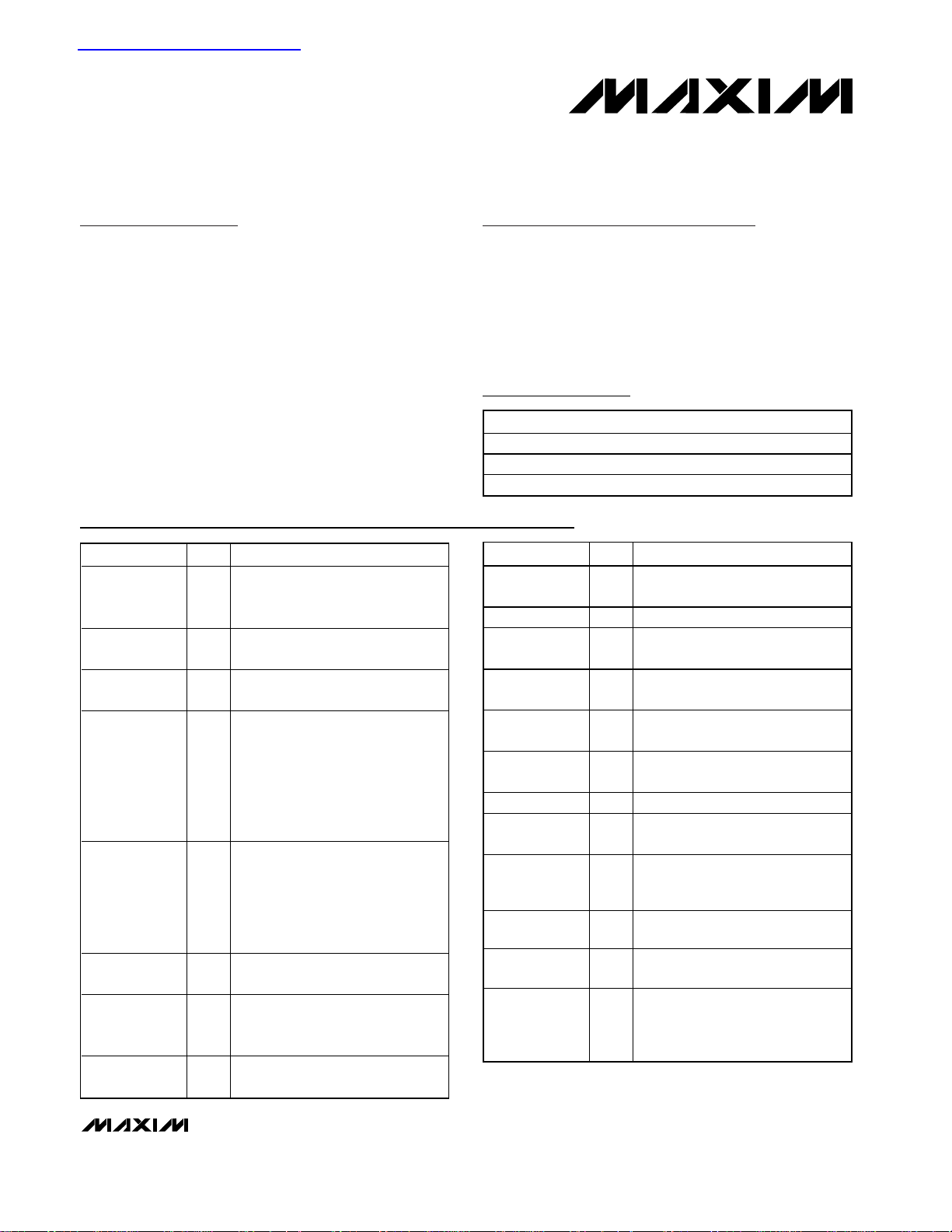
MAX2825 Component List
For pricing, delivery, and ordering information, please contact Maxim/Dallas Direct! at
1-888-629-4642, or visit Maxim’s website at www.maxim-ic.com.
Ordering Information
查询MAX2825EVKIT供应商
DESIGNATION QTY DESCRIPTION
C1, C8, C14,
C15, C31, C44,
C48, C49, C61
C2, C12, C13 3
C4 1
C5, C7, C10,
C11, C17, C18,
C21, C22, C29,
C35, C37, C40,
C42, C43, C45,
C46, C50, C52,
C54, C59, C60
C6, C9, C16,
C19, C20,
C23–C28, C30,
C32, C36, C38,
C41, C56,
C57, C58
C33, C34 2
C39, C51, C53,
C55
C47 1
9 Open
10pF ±0.1pF 0402 capacitors
Murata GJ61555C1H100B
1.0pF ±0.1pF 0402 capacitor
Murata GJ61555C1H1R0B
0.1µF ±10% 0402 capacitors
21
Murata GRP155R61A104K
0.01µF ±10% 0402 capacitors
17
Murata GRP155R71C103K
330pF ±10% 0402 capacitors
Murata GRP155R71H331K
10µF ±10% tantalum capacitors—
4
A case
AVX TAJA106K010
100pF ±5% 0402 capacitor
Murata GRP1555C1H101B
PART TEMP RANGE IC PACKAGE
MAX2825EVKIT -40°C to +85°C 56 Thin QFN
MAX2826EVKIT -40°C to +85°C 56 Thin QFN
MAX2827EVKIT -40°C to +85°C 56 Thin QFN
DESIGNATION QTY DESCRIPTION
J1, J4,
J5–J9
J2, J3 2 Open
J12–J16 5
J18 1
JP21, JP22 2
L1 1
L3, L4, L5 3 Open
L6 1
R1, R2, R6,
R10, R16, R17,
R22, R27
R3, R7, R18,
R23, R25
R4, R5,
R21, R26
R8, R9, R12,
R13, R28, R29,
R31, R32,
R36, R42
SMA edge-mount—round contacts
7
Johnson 142-0701-801
1 x 2 headers
Sullins PTC36SAAN
DB25, right angle—male
AMP 747238-4
1 x 3 headers
Sullins PTC36SAAN
6.8nH ±5% 0402 inductor
Murata LQG15HN6R8J00
3.9nH ±0.2nH 0402 inductor
Murata LQP15MN3N9C00
875Ω ±1% 0402 resistors
5 10kΩ ±1% 0402 resistors
4 49.9Ω ±1% 0402 resistors
10 0Ω ±5% 0402 resistors
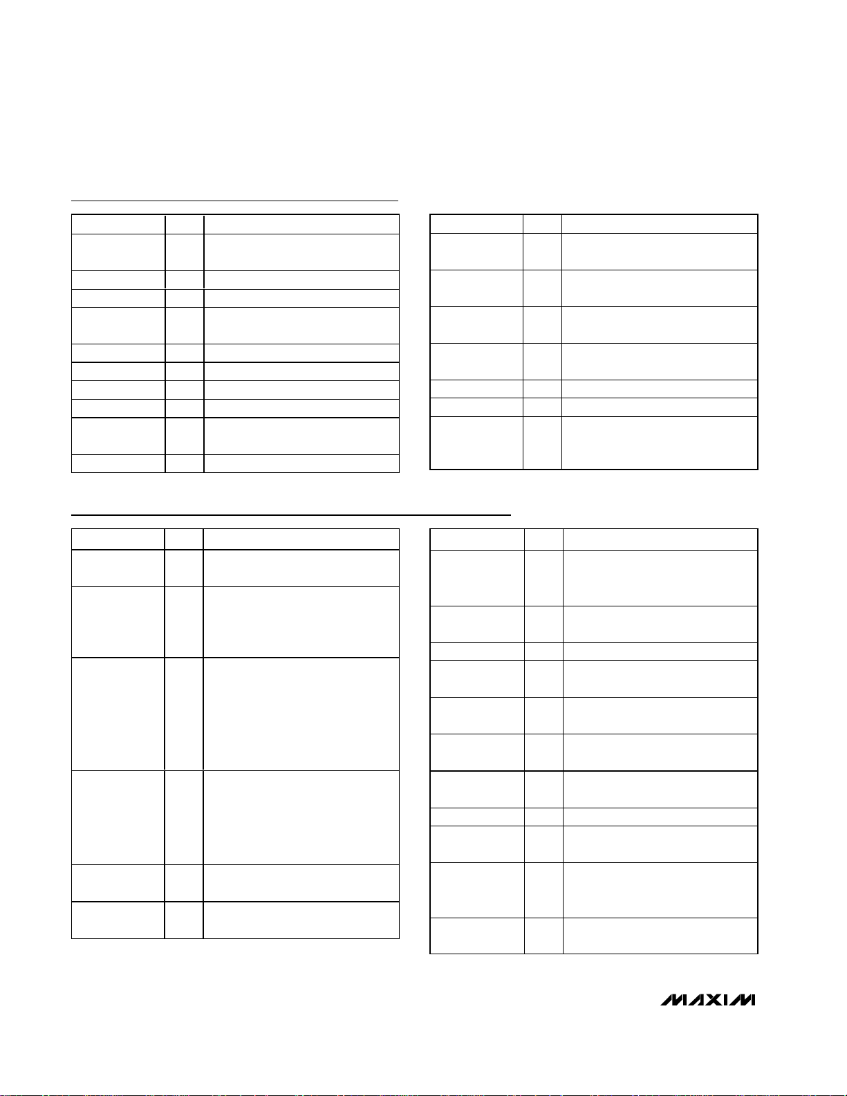
Page 2
Evaluate: MAX2825/MAX2826/MAX2827
MAX2825/MAX2826/MAX2827 Evaluation Kits
2 _______________________________________________________________________________________
MAX2825 Component List (continued)
MAX2826 Component List
DESIGNATION QTY DESCRIPTION
R11, R30, R33,
R35, R38
R14 1 267Ω ±1% 0402 resistor
R15 1 11kΩ ±1% 0402 resistor
R19 1
R20, R24 2 365Ω ±1% 0402 resistors
R34, R37 2 100kΩ ±1% 0402 resistors
R39, R40, R41 3 100Ω ±1% 0402 resistors
R43 1 1kΩ ±1% 0402 resistor
T1 1
T2 1 Open
5 Open
EMI filter ±0.2nH (0603)
Murata BLM18AG221SN1D
SMD balun
Murata LDB182G4510C-110
DESIGNATION QTY DESCRIPTION
TP1–TP8,
TP10–TP23
U1, U5 2
U2, U6 2
U3 1
U4 1 Maxim MAX2827ETN
U7 1 Open
U8, U9 2
Test points
22
Keystone 5000
Differential line drivers
Maxim MAX4447ESE
Line receivers
Maxim MAX4444ESE
LDO
Maxim MAX6061BEUR
Octal buffer/driver
Texas Instruments
SN74LVTH244ADBR
DESIGNATION QTY DESCRIPTION
C1 1
C2, C4, C8,
C12, C13, C31,
C44, C48,
C49, C61
C5, C7, C10,
C11, C17, C18,
C21, C22, C29,
C35, C37, C40,
C42, C43, C45,
C46, C50, C52,
C54, C59, C60
C6, C9, C16,
C19, C20,
C23–C28, C30,
C32, C36, C38,
C41, C56, C57,
C58
C14, C15 2
C33, C34 2
0.75pF ±0.1pF 0402 capacitor
Murata GRM1555C1HR75B
10 Open
0.1µF ±10% 0402 capacitors
21
Murata GRP155R61A104K
0.01µF ±10% 0402 capacitors
17
Murata GRP155R71C103K
1.2pF ±0.1pF 0402 capacitors
Murata GJ61555C1H1R2B
330pF ±10% 0402 capacitors
Murata GRP155R71H331K
DESIGNATION QTY DESCRIPTION
C39, C51,
C53, C55
C47 1
J1, J4 2 Open
J2, J3, J5–J9 7
J12–J16 5
J18 1
JP21, JP22 2
L1, L3, L4, L6 4 Open
L5 1
R1, R2, R6,
R10, R16, R17,
R22, R27
R3, R7, R18,
R23, R25
10µF ±10% tantalum capacitors—
A case
4
AVX TAJA106K010
100pF ±5% 0402 capacitor
Murata GRP1555C1H101B
SMA edge-mount—round contacts
Johnson 142-0701-801
1 x 2 headers
Sullins PTC36SAAN
DB25, right angle—male
AMP 747238-4
1 x 3 headers
Sullins PTC36SAAN
4.3nH ±0.2nH 0402 inductor
Murata LQP15MN4N3C00
875Ω ±1% 0402 resistors
5 10kΩ ±1% 0402 resistors
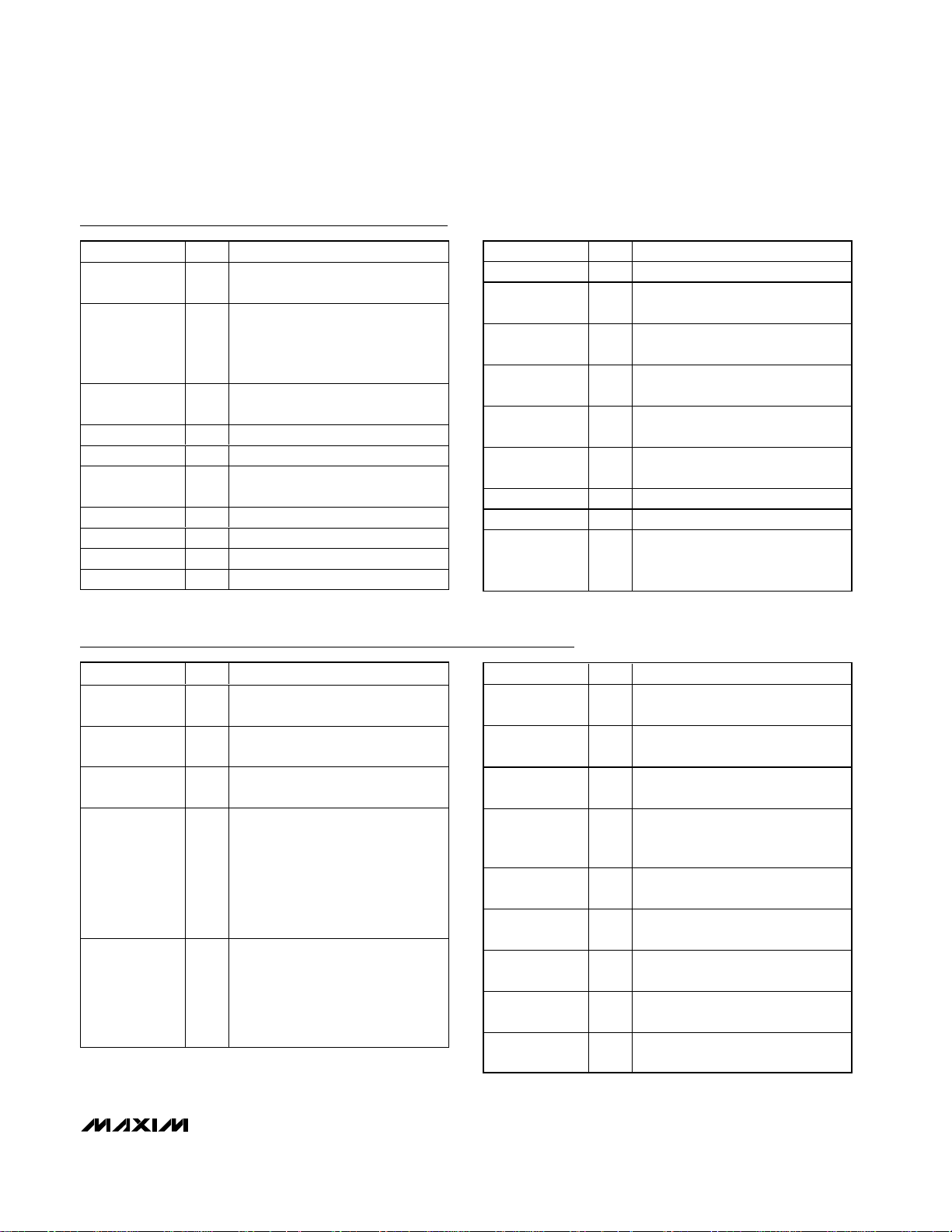
Page 3
Evaluate: MAX2825/MAX2826/MAX2827
MAX2825/MAX2826/MAX2827 Evaluation Kits
_______________________________________________________________________________________ 3
MAX2827 Component List
MAX2826 Component List (continued)
DESIGNATION QTY DESCRIPTION
R4, R5,
R21, R26
R8, R9, R12,
R13, R28, R29,
R31, R32,
R36, R42
R11, R30, R33,
R35, R38
R14 1 267Ω ±1% 0402 resistor
R15 1 11kΩ ±1% 0402 resistor
R19 1
R20, R24 2 365Ω ±1% 0402 resistors
R34, R37 2 100kΩ ±1% 0402 resistors
R39, R40, R41 3 100Ω ±1% 0402 resistors
R43 1 1kΩ ±1% 0402 resistor
DESIGNATION QTY DESCRIPTION
C1 1
C2, C12, C13 3
C4 1
C5, C7, C10,
C11, C17, C18,
C21, C22, C29,
C35, C37, C40,
C42, C43, C45,
C46, C50, C52,
C54, C59, C60
C6, C9, C16,
C19, C20,
C23–C28, C30,
C32, C36, C38,
C41, C56,
C57, C58
4 49.9Ω ±1% 0402 resistors
10 0Ω ±5% 0402 resistors
5 Open
EMI filter ±0.2nH (0603)
Murata BLM18AG221SN1D
0.75pF ±0.1pF 0402 capacitor
Murata GRM1555C1HR75B
10pF ±0.1pF 0402 capacitors
Murata GJ61555C1H100B
1.0pF ±0.1pF 0402 capacitor
Murata GJ61555C1H1R0B
0.1µF ±10% 0402 capacitors
21
Murata GRP155R61A104K
0.01µF ±10% 0402 capacitors
17
Murata GRP155R71C103K
DESIGNATION QTY DESCRIPTION
T1 1 Open
T2 1
TP1–TP8,
TP10–TP23
U1, U5 2
U2, U6 2
U3 1
U4 1 Maxim MAX2827ETN
U7 1 Open
U8, U9 2
SMD balun
Murata LDB215G2505C-001
Test points
22
Keystone 5000
Differential line drivers
Maxim MAX4447ESE
Line receivers
Maxim MAX4444ESE
LDO
Maxim MAX6061BEUR
Octal buffer/driver
Texas Instruments
SN74LVTH244ADBR
DESIGNATION QTY DESCRIPTION
C8, C31, C44,
C48, C49, C61
C14, C15 2
C33, C34 2
C39, C51, C53,
C55
C47 1
J1–J9 9
J12–J16 5
J18 1
JP21, JP22 2
14 Open
1.2pF ±0.1pF 0402 capacitors
Murata GJ61555C1H1R2B
330pF ±10% 0402 capacitors
Murata GRP155R71H331K
10µF ±10% tantalum capacitors—
4
A case
AVX TAJA106K010
100pF ±5% 0402 capacitor
Murata GRP1555C1H101B
SMA edge-mount—round contacts
Johnson 142-0701-801
1 x 2 headers
Sullins PTC36SAAN
DB25, right angle—male
AMP 747238-4
1 x 3 headers
Sullins PTC36SAAN
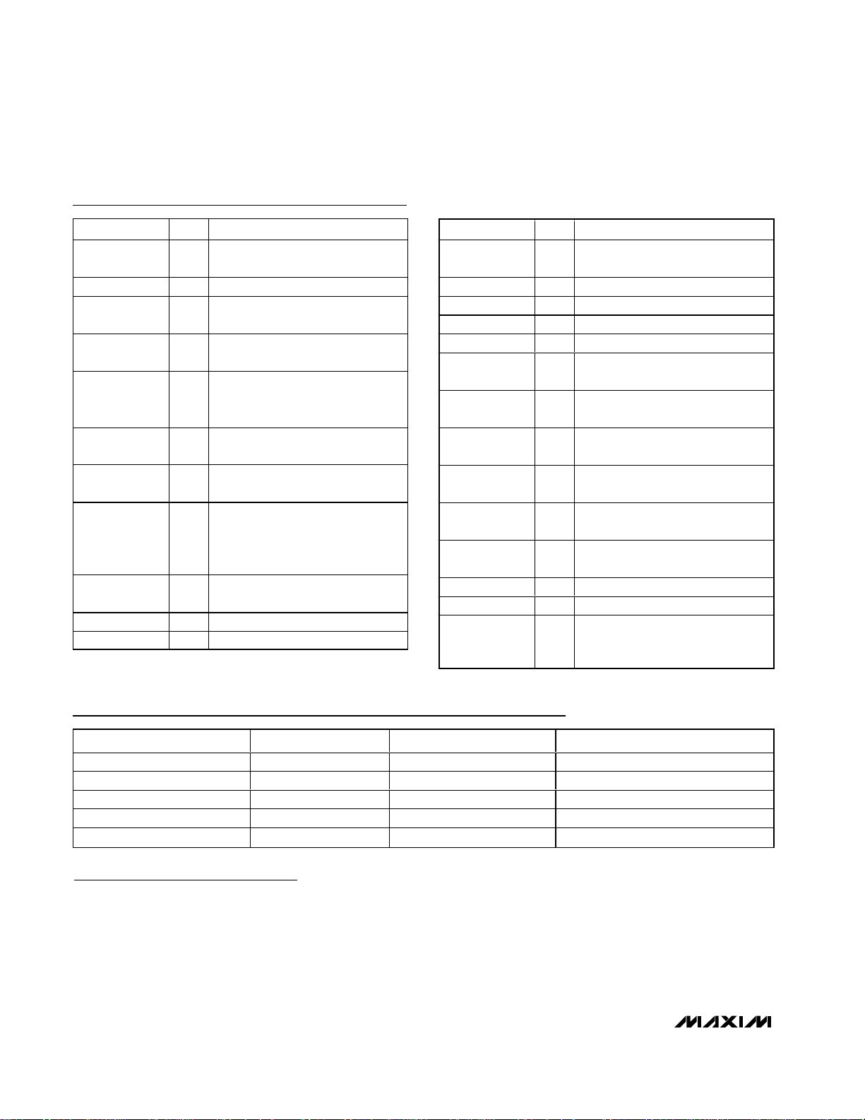
Page 4
Evaluate: MAX2825/MAX2826/MAX2827
MAX2825/MAX2826/MAX2827 Evaluation Kits
4 _______________________________________________________________________________________
Quick Start
Each EV kit is fully assembled and factory tested.
Follow the instructions in the Connections and Setup
section to test the device.
Test Equipment Required
This section lists the recommended test equipment to
verify the operation of the MAX2825/MAX2826/
MAX2827. It is intended as a guide only, and substitutions may be possible.
• DC supply capable of delivering +5.0V and 200mA
of continuous current
• DC supply capable of delivering -5.0V and 200mA of
continuous current
• DC supply capable of delivering +3.6V and 400mA
of continuous current
MAX2827 Component List (continued)
Component Suppliers
DESIGNATION QTY DESCRIPTION
L1 1
L3, L4 2 Open
L5 1
L6 1
R1, R2, R6,
R10, R16, R17,
R22, R27
R3, R7, R18,
R23, R25
R4, R5, R21,
R26
R8, R9, R12,
R13, R28, R29,
R31, R32,
R36, R42
R11, R30, R33,
R35, R38
R14 1 267Ω ±1% 0402 resistor
R15 1 11kΩ ±1% 0402 resistor
6.8nH ±5% 0402 inductor
Murata LQG15HN6R8J00
4.3nH ±0.2nH 0402 inductor
Murata LQP15MN4N3C00
3.9nH ±0.2nH 0402 inductor
Murata LQP15MN3N9C00
875Ω ±1% 0402 resistors
5 10kΩ ±1% 0402 resistors
4 49.9Ω ±1% 0402 resistors
10 0Ω ±5% 0402 resistors
5 Open
DESIGNATION QTY DESCRIPTION
R19 1
R20, R24 2 365Ω ±1% 0402 resistors
R34, R37 2 100kΩ ±1% 0402 resistors
R39, R40, R41 3 100Ω ±1% 0402 resistors
R43 1 1kΩ ±1% 0402 resistor
T1 1
T2 1
TP1–TP8,
TP10–TP23
U1, U5 2
U2, U6 2
U3 1
U4 1 Maxim MAX2827ETN
U7 1 Open
U8, U9 2
EMI filter ±0.2nH (0603)
Murata BLM18AG221SN1D
SMD balun
Murata LDB182G4510C-110
SMD balun
Murata LDB215G2505C-001
Test points
22
Keystone 5000
Differential line drivers
Maxim MAX4447ESE
Line receivers
Maxim MAX4444ESE
LDO
Maxim MAX6061BEUR
Octal buffer/driver
Texas Instruments
SN74LVTH244ADBR
SUPPLIER PHONE FAX WEBSITE
AVX 843-448-9411 843-448-1943 www.avx.com
Digi-Key 800-344-4539 218-681-3380 www.digikey.com
Johnson Components 800-247-8256 507-833-6287 www.johnsoncomponents.com
Murata 770-436-1300 770-436-3030 www.murata.com
Texas Instruments ——www.ti.com
Page 5

Evaluate: MAX2825/MAX2826/MAX2827
MAX2825/MAX2826/MAX2827 Evaluation Kits
_______________________________________________________________________________________ 5
Windows is a registered trademark of Microsoft.
• HP8663A or equivalent low-noise signal source
capable of generating a 20MHz or 40MHz reference
oscillator signal
• Two HP8648 or equivalent signal sources capable of
generating 0dBm up to 6GHz
• 802.11x I/Q waveform generator (optional)
• HP8561E or equivalent RF spectrum analyzer with a
minimum frequency range of 100kHz to 6GHz
• TDS3012 or equivalent oscilloscope with 200MHz
bandwidth
• IBM PC or compatible with Windows95/98/2000/NT
4.0, or later operating system and an available parallel port
• Male-to-female 25-pin parallel cable, straight through
Connections and Setup
This section provides step-by-step instructions for getting the EV kit up and running in all modes:
1) Install and run the MAX2825/MAX2826/MAX2827
control software.
2) To control the EV kit through the 3-wire interface,
connect the male-to-female 25-pin parallel cable
between the PC and EV kit.
3) With the power supply turned off, connect a +2.7V
power supply to the header labeled VCC (J13).
Connect the power-supply ground to the header
labeled GND (J12).
4) With the power supply turned off, connect a +5V
power supply to the header labeled +5V (J16), and
a -5V power supply to the header labeled -5V (J14).
Connect the power-supply ground to the header
labeled GND (J21).
5) Connect the low-noise signal source to FREF (J9).
6) Turn on the +5V and -5V power supplies, followed
by the +2.7V power supply. Set the low-noise signal
source to 20MHz and 2dBm. Enable the signal
source. The lock indicator should be green.
Receive Mode
To evaluate the devices in receive mode:
1) Set the RXON jumper (JP22) to the On position and
the TXON jumper (JP21) to the Off position.
2) Connect the RF signal source to either RXRFL
(802.11g, J4) or RXRFH (802.11a, J3). Set the RF frequency to 2437MHz (802.11g) or 5.25GHz (802.11a).
Set the signal power to -100dBm.
3) Set the register setting to the default values listed in
the MAX2825/MAX2826/MAX2827 data sheet. Use
the software to select between 802.11g and 802.11a
modes. In the program, set the frequency to either
2442MHz (802.11g) or 5.255GHz (802.11a). Set the
RX gain to maximum using either the slider bar or
the control bits.
4) Connect the spectrum analyzer to either RXBBI or
RXBBQ. Set the center frequency to 5MHz with a
10MHz span.
5) Turn on the RF signal source. The output at 5MHz
should be approximately -4dBm (802.11g) or -5dBm
(802.11a).
Transmit Mode
To evaluate the devices in transmit mode:
1) Set the TXON jumper (JP21) to the On position and
the RXON jumper (JP22) to the Off position.
2) Connect a 2MHz I/Q signal to TXBBQ and TXBBI.
Set the input amplitude of each channel to
100mV
RMS
.
3) Set the register setting to the default values listed in
the MAX2825/MAX2826/MAX2827 data sheet. Use
the software to select between 802.11g and
802.11a modes. In the program, set the frequency
to either 2437MHz (802.11g) or 5.25GHz (802.11a).
Set the TX gain to maximum using either the slider
bar or the control bits.
4) Connect the spectrum analyzer to either TXRFL
(802.11g, J1) or TXRFH (802.11a, J2).
5) Turn on the baseband signal sources. The output at
RF should be approximately -2dBm (802.11g) or
-4dBm (802.11a).
Layout Considerations
The MAX2825/MAX2826/MAX2827 EV kits can serve as
guides for board layout. Keep PC board trace lengths
as short as possible to minimize parasitic inductance.
Also, keep decoupling capacitors as close to the IC as
possible with a direct connection to the ground plane.
Please refer to the MAX2825/MAX2826/MAX2827 data
sheet for more detailed information. Gerber files for
these EV kits can be requested at www.maxim-ic.com.
Page 6

Evaluate: MAX2825/MAX2826/MAX2827
MAX2825/MAX2826/MAX2827 Evaluation Kits
6 _______________________________________________________________________________________
Figure 1. MAX2825/MAX2826/MAX2827 EV Kit Schematics
Page 7

Evaluate: MAX2825/MAX2826/MAX2827
MAX2825/MAX2826/MAX2827 Evaluation Kits
_______________________________________________________________________________________ 7
Figure 2. MAX2825/MAX2826/MAX2827 EV Kit PC Board Layout—Top Silkscreen
1.0"
Page 8

Evaluate: MAX2825/MAX2826/MAX2827
MAX2825/MAX2826/MAX2827 Evaluation Kits
8 _______________________________________________________________________________________
Figure 3. MAX2825/MAX2826/MAX2827 EV Kit PC Board Layout—Component Side
1.0"
Page 9

Evaluate: MAX2825/MAX2826/MAX2827
MAX2825/MAX2826/MAX2827 Evaluation Kits
_______________________________________________________________________________________ 9
Figure 4. MAX2825/MAX2826/MAX2827 EV Kit PC Board Layout—Inner Layer 2, Gound Layer
1.0"
Page 10

Evaluate: MAX2825/MAX2826/MAX2827
MAX2825/MAX2826/MAX2827 Evaluation Kits
10 ______________________________________________________________________________________
Figure 5. MAX2825/MAX2826/MAX2827 EV Kit PC Board Layout—Inner Layer 3, Routes
1.0"
Page 11

Evaluate: MAX2825/MAX2826/MAX2827
MAX2825/MAX2826/MAX2827 Evaluation Kits
______________________________________________________________________________________ 11
Figure 6. MAX2825/MAX2826/MAX2827 EV Kit PC Board Layout—Solder Side
1.0"
Page 12

Maxim cannot assume responsibility for use of any circuitry other than circuitry entirely embodied in a Maxim product. No circuit patent licenses are
implied. Maxim reserves the right to change the circuitry and specifications without notice at any time.
12 ____________________Maxim Integrated Products, 120 San Gabriel Drive, Sunnyvale, CA 94086 408-737-7600
© 2003 Maxim Integrated Products Printed USA is a registered trademark of Maxim Integrated Products.
Evaluate: MAX2825/MAX2826/MAX2827
MAX2825/MAX2826/MAX2827 Evaluation Kits
Figure 7. MAX2825/MAX2826/MAX2827 EV Kit PC Board Layout—Bottom Silkscreen
1.0"
 Loading...