

Page 1
General Description
The MAX2754 self-contained, linear modulation, voltage-controlled oscillator (VCO) is intended for use in
the 2.4GHz to 2.5GHz ISM band, particularly for FSK
modulation systems that utilize a direct frequency-modulation transmit architecture. This device features a linear modulation input in addition to the standard
frequency tuning input. The frequency tuning range of
1145MHz to 1250MHz (1/2 LO) also supports an IF up
to 110MHz with low side LO. The VCO is based on
Maxim’s proprietary monolithic VCO technology, where
all VCO components are integrated on-chip, including
the varactor and inductor.
The MAX2754 linear modulation input offers a means to
directly FM modulate the VCO with a constant modulation sensitivity over the tuning voltage input range.
Typical frequency deviation is -500kHz/V which is linear
to ±4% over the guaranteed frequency limits. The tuning input voltage range is +0.4V to +2.4V and the oscillator frequency is factory adjusted to provide
guaranteed limits. The oscillator signal is buffered by
an output amplifier stage (internally matched to 50Ω) to
provide higher output power and isolate the oscillator
from load impedance variations.
The MAX2754 operates over a +2.7V to +5.5V supply
range. This device also provides a digitally controlled
shutdown mode to permit implementation of sophisticated power-supply management. In shutdown, the
supply current is reduced to 0.2µA. Even when active,
power consumption is a modest 41mW.
The MAX2754 is packaged in the miniature 8-pin µMAX
to offer the world’s smallest, complete 2.4GHz directmodulation VCO solution.
Applications
HomeRF WLAN
Bluetooth
2.4GHz Cordless Phones
2.4GHz Wireless Data Radios
Features
♦ Fully Monolithic VCO Construction with On-Chip
Inductor and Varactor Tuning Elements
♦ Guaranteed 1145MHz to 1250MHz Tuning Range
to Support 1/2 LO Applications
♦ Modulation Linearity Within ±4%
♦ Precise Modulation Gain (-500kHz/V)
♦ Low Phase Noise (-137dBc/Hz at 4MHz offset)
♦ +2.7V to +5.5V Single-Supply Operation
♦ Low-Current Shutdown Mode
♦ Miniature 8-Pin µMAX
®
Package
MAX2754
1.2GHz VCO with Linear
Modulation Input
________________________________________________________________ Maxim Integrated Products 1
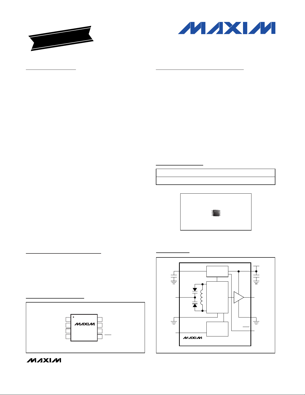
Pin Configuration
Ordering Information
SHDN
GND2
OUT
V
CC
V
CC
MOD
GND1
TUNE
TUNE
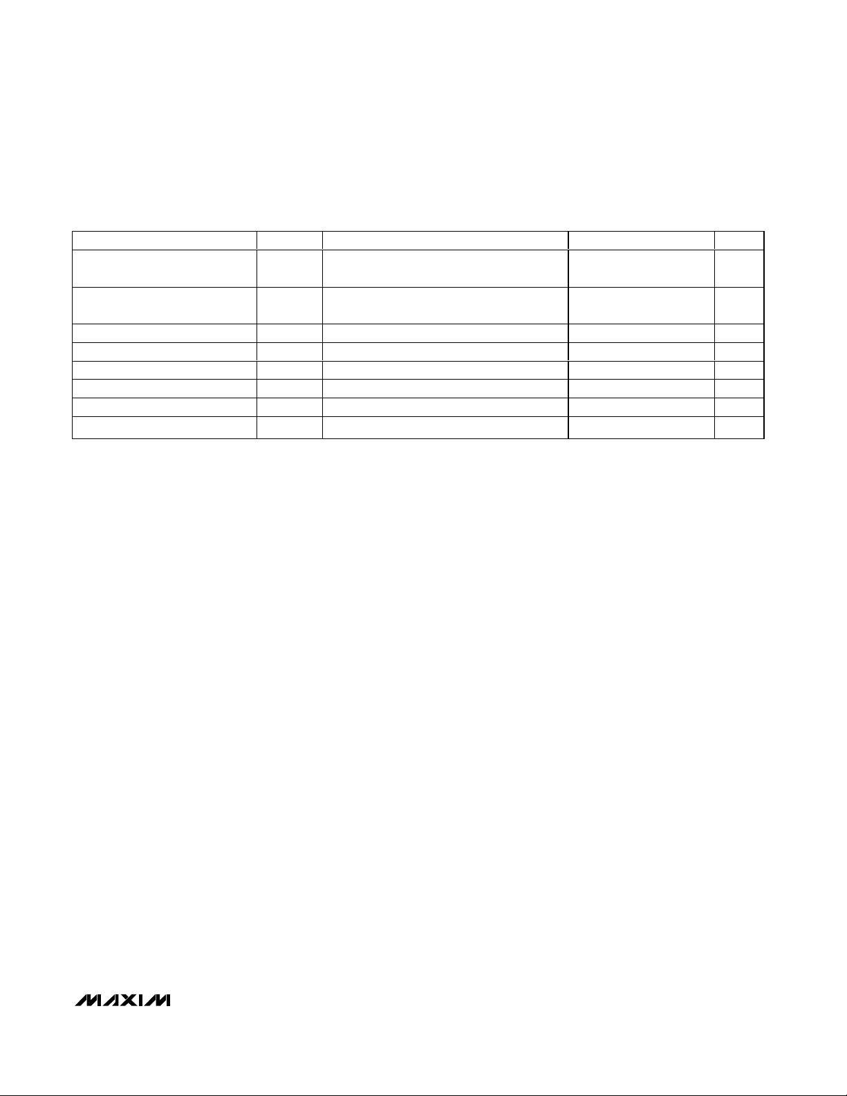
VREG
330nF
OUT TO
MIXER/
SYNTHESIZER
330nF
MODULATION
VOLTAGE
SIGNAL
MAX2754
REG AND BIAS
OSCILLATOR
CORE
LINEAR
MODULATION
INTERFACE
SHDN
Typical Operating Circuit
19-2102; Rev 2; 5/06
For pricing, delivery, and ordering information, please contact Maxim/Dallas Direct! at
1-888-629-4642, or visit Maxim’s website at www.maxim-ic.com.
(3mm ✕5mm)
8-pin µMAX
EVALUATION KIT
AVAILABLE
µMAX is a registered trademark of Maxim Integrated Circuits, Inc.
PART TEMP RANGE PIN-PACKAGE
MAX2754EUA -40°C to +85°C 8 µMAX
TOP VIEW
1
VREG
2
TUNE
GND1
MAX2754
3
4
µMAX
8
V
CC
7
OUT
6
GND2
5
SHDNMOD
Page 2
MAX2754
1.2GHz VCO with Linear
Modulation Input
2 _______________________________________________________________________________________
ABSOLUTE MAXIMUM RATINGS
DC ELECTRICAL CHARACTERISTICS
(VCC= +2.7V to +5.5V, V
TUNE
= +0.4V to +2.4V, V
SHDN
≥ +2.0V, V
MOD
= +1.4V, OUT is connected to a 50Ω load, TA= -40°C to
+85°C. Typical values are at V
CC
= +3.0V, TA= +25°C, unless otherwise noted.) (Note 1)
Stresses beyond those listed under “Absolute Maximum Ratings” may cause permanent damage to the device. These are stress ratings only, and functional
operation of the device at these or any other conditions beyond those indicated in the operational sections of the specifications is not implied. Exposure to
absolute maximum rating conditions for extended periods may affect device reliability.
VCCto GND...........................................................-0.3V to +6.0V
VREG to GND ........................................................-0.3V to +6.0V
TUNE, SHDN, MOD to GND.......................-0.3V to (V
CC
+ 0.3V)
OUT to GND ..........................................................-0.3V to +6.0V
Continuous Power Dissipation (T
A
= +70°C)
8-Pin µMAX (derate 5.7mW/°C above T
A
= +70°C) ....457mW
Operating Temperature Range ...........................-40°C to +85°C
Junction Temperature......................................................+150°C
Storage Temperature Range .............................-65°C to +160°C
Lead Temperature (soldering, 10s) .................................+300°C
AC ELECTRICAL CHARACTERISTICS
(MAX2754 EV kit. VCC= +2.7V to +5.5V, V
TUNE
= +0.4V to +2.4V, V
SHDN
≥ +2.0V, V
MOD
= +1.4V, OUT is connected to a 50Ω load,
T
A
= +25°C. Typical values are at VCC= +3.0V, TA= +25°C, unless otherwise noted.) (Note 1)
CAUTION! ESD SENSITIVE DEVICE
Supply Voltage V
Supply Current I
Digital Input Voltage High V
Digital Input Voltage Low V
Digital Input Current High I
Digital Input Current Low I
Modulation Input Voltage Range V
TUNE Leakage Current (Note 2) V
PARAMETER SYMBOL CONDITIONS MIN TYP MAX UNITS
CC
T
A
T
CC
IH
IL
IH
IL
MOD
A
V
SHDN
V
SHDN
V
SHDN
TUNE
= +25°C, V
= -40°C to +85°C, V
≤ 0.6V -2 0.2 2 µA
≥ 2.0V -2 2 µA
≤ 0.6V -1 1 µA
= +0.4V to +2.4V 0.01 nA
2.7 5.5 V
≥ 2.0V 13.7 19
SHDN
≥ 2.0V 20
SHDN
2.0 V
0.6 V
0.4 2.4 V
mA
Oscillator Guaranteed Frequency
Limits
PARAMETER SYMBOL CONDITIONS MIN TYP MAX UNITS
f
MIN
f
MAX
Phase Noise
Tuning Gain
,
V
= +0.4V to +2.4V,
TUNE
T
= -40°C to +85°C
A
f
= 4MHz -137 dBc/Hz
OFFSET
Noise floor -151 dBm/Hz
V
at f
V
TUNE
TUNE
at f
MIN
MAX
1145 1250 MHz
124
81
MHz/V
Output Power -5 dBm
Modulation Peak Frequency
Deviation
Modulation Sensitivity Common-mode V
f
MIN
< f < f
(Note 2) ±400 ±500 ±600 kHz
MAX
= 1.4V -500 kHz/V
MOD
Page 3
MAX2754
1.2GHz VCO with Linear
Modulation Input
_______________________________________________________________________________________ 3
Note 1: Specifications are production tested at TA= +25°C. Limits over temperature are guaranteed by design and characterization.
Note 2: Limits are guaranteed by production test at +25°C.
Note 3: Center point is nominally +1.4V.
Note 4: Maximum variation in the modulation sensitivity from its average value over the guaranteed frequency limits.
Note 5: Bandwidth is defined as the point where the response to the modulation port is 0.707 times the low-frequency response.
Bandwidth limits on the modulation input for a 1Vp-p sine wave. Common-mode V
MOD
= +1.4V.
Note 6: Refer to Output Buffer section for suggestions to improve the return loss to 12dB.
Note 7: Turn-on time to within 3dB of final output power.
Note 8: Turn-off time to output power of -10dBm.
AC ELECTRICAL CHARACTERISTICS (continued)
(MAX2754 EV kit. VCC= +2.7V to +5.5V, V
TUNE
= +0.4V to +2.4V, V
SHDN
≥ +2.0V, V
MOD
= +1.4V, OUT is connected to a 50Ω load,
T
A
= +25°C. Typical values are at VCC= +3.0V, TA= +25°C, unless otherwise noted.) (Note 1)
p-p
PARAMETER SYMBOL CONDITIONS MIN TYP MAX UNITS
Modulation Linearity
Modulation Full-Power Bandwidth
(Note 5)
Return Loss (Note 6) f
V
MOD
f
< f < f
MIN
= +0.4 to +2.4V,
(Note 4)
MAX
±4 %
2.5 MHz
MIN
< f < f
MAX
7.5 dB
Output Harmonics -20 dBc
Load Pulling VSWR = 2:1, all phases 1.5 MHz
Supply Pushing V
stepped: +3.3V to +2.8V 0.16 MHz/V
CC
Oscillator Turn-On Time (Note 7) 10 µs
Oscillator Turn-Off Time (Note 8) 8 µs
Page 4

MAX2754
1.2GHz VCO with Linear
Modulation Input
4 _______________________________________________________________________________________
Typical Operating Characteristics
(MAX2754 EV kit, VCC= +3.0V, V
SHDN
≥ +2.0V, V
TUNE
= V
MOD
= +1.4V, and TA= +25°C, unless otherwise noted.)
VCO TUNING CURVE
1350
1300
1250
1200
1150
1100
FREQUENCY (MHz)
1050
1000
950
01.00.5 1.5 2.0 2.5 3.0
TA = -40°C
TA = +85°C
V
TUNE
TA = +25°C
(V)
-400
-420
MAX2754 toc01
-440
-460
-480
-500
-520
-540
-560
MODULATION SENSITIVITY (kHz/V)
-580
-600
1140 11801160 1200 1220 1240 1260
MODULATION SENSITIVITY vs.
CARRIER FREQUENCY
1.0
MAX2754 toc02
TA = -40°C
TA = +85°C
CARRIER FREQUENCY (MHz)
TA = +25°C
0.8
0.6
0.4
TUNING INPUT CURRENT (nA)
0.2
0
-40 10-15 35 60 85
TUNE INPUT CURRENT
vs. TEMPERATURE
MAX2754 toc03
TEMPERATURE (°C)
OUTPUT POWER vs. FREQUENCY
-3.0
-3.5
-4.0
-4.5
-5.0
OUTPUT POWER (dBm)
-5.5
-6.0
VCC = +5.5V
VCC = +4.0V
VCC = +2.7V
1140 1240 1260
11801160 1200 1220
FREQUENCY (MHz)
PHASE NOISE
-60
-70
-80
-90
-100
-110
-120
PHASE NOISE (dBc/Hz)
-130
-140
-150
-160
10 100 1000 10,000
OFFSET FREQUENCY (kHz)
-2
MAX2754 toc04
-3
-4
-5
-6
OUTPUT POWER (dBm)
-7
-8
1140 1200 12201160 1180 1240 1260
0
-10
MAX2754 toc07
-20
-30
-40
-50
-60
OUTPUT POWER (dBm)
-70
-80
-90
-100
OUTPUT POWER
vs. FREQUENCY
TA = +85°C
TA = +25°C
TA = -40°C
FREQUENCY (MHz)
OSCILLATOR TURN-ON/
TURN-OFF TIME
SHDN LOW-TO-HIGH
AT TIME = 0
SHDN HIGH-TO-LOW
AT TIME = 0
02010 30 40 50
TIME (µs)
MAX2754 toc05
MAX2754 toc08
NORMALIZED HARMONIC
OUTPUT SPECTRUM
∆ = -20dBc
OUTPUT POWER (dBm)
ƒ
O
FREQUENCY
OUTPUT S
0
-5
(dB)
-10
11
S
-15
-20
800 1000 1200 1400900 1100 1300 1500 1600
FREQUENCY (MHz)
2ƒ
O
11
∆ = -30dBc
3ƒ
MAX2754 toc06
O
MAX2754 toc09
Page 5

Detailed Description
Oscillator
The MAX2754 VCO is implemented as an LC oscillator
topology, integrating all of the tank components onchip. This fully monolithic approach provides an
extremely easy-to-use VCO, equivalent to a VCO module. The frequency is controlled by a voltage applied to
the TUNE pin. The VCO core uses a differential topology to provide a stable frequency versus supply voltage
and improve the immunity to load variations. In addition, there is a buffer amplifier following the oscillator
core to provide added isolation from load and supply
variations and to boost the output power.
Linear Modulation
The linear modulation input offers a means to directly
FM modulate the VCO with a controlled amount of frequency deviation for a given input voltage deviation.
The unique technique maintains a consistent modulation gain (df/dV
MOD
) across the entire frequency tuning
range of the part, enabling accurate FM modulation
derived solely from the filtered NRZ “data” stream (the
modulation voltage input).
The modulation input is single-ended and centered
about +1.4V. The linear modulation full-scale range is
±1V around this point, for a +0.4V to +2.4V input voltage range. A very important point to note is that the
sign of the modulation gain is negative. A positive
change in V
MOD
results in a negative change in oscilla-
tion frequency. This convention for the modulation gain
is due to the practical implementation of the internal linearizing circuitry. This gain inversion must be considered when designing the analog voltage interface that
drives the linear modulation input. The easiest way to
handle this is to invert the logic polarity of the modulation data three-state output buffer (TX data output).
Where it is impossible to invert the data-stream logic
polarity, an external inverter and three-state buffer
would be required. These devices are offered in small
single-logic gates in SC-79 style packages from various
manufacturers (e.g., Fairchild—Tiny Logic, On
Semiconductor, or Rohm).
Figure 1 illustrates the frequency versus V
MOD
characteristic of the modulation input. Note the negative slope
of the curve, df
MOD
/dV
MOD
< 0, where f
MOD
= f
OUT
-
f
NOM
.
Output Buffer
The oscillator signal from the core drives an output
buffer amplifier. The amplifier is internally matched to
50Ω including an on-chip DC-blocking capacitor. The
return loss can be improved to a minimum of 12dB over
1145MHz to 1250MHz by adding a 2.5nH series inductor and a 3.0pF shunt capacitor. The output buffer has
a ground connection separate from the oscillator core
to minimize load-pulling effects. The amplifier boosts
the oscillator signal to a level suitable for driving most
RF mixers.
MAX2754
1.2GHz VCO with Linear
Modulation Input
_______________________________________________________________________________________ 5
Pin Description
PIN NAME FUNCTION
1 VREG Capacitor Connection to the On-Chip Linear Regulator Output. Connect a 330nF capacitor to ground.
2 TUNE
3 GND1
4 MOD Linear Modulation Input. High-impedance CMOS input with a voltage range of +0.4V to +2.4V.
5 SHDN
6 GND2
7 OUT
8V
CC
Oscillator Frequency Tuning-Voltage Input. High-impedance input with a voltage range of +0.4V (low
frequency) to +2.4V (high frequency).
Ground Connection for the Oscillator Core. Requires a low-inductance connection to the circuitboard ground plane.
Shutdown Input. Drive logic low to place the device in shutdown mode. Drive logic high for normal
operation.
Ground Connection for Output-Buffered Amplifier, Linear Modulation Interface, and Biasing.
Requires a low-inductance connection to the circuit-board ground plane.
Buffered Oscillator Output. Incorporates an internal DC-blocking capacitor. OUT is internally
matched to 50Ω.
Supply Voltage Connection. Requires external RF bypass capacitor to ground for low noise and low
spurious content performance from the oscillator. Bypass with a 330pF capacitor to ground.
Page 6

MAX2754
Applications Information
Tune Input
The tuning input is typically connected to the output of
the PLL loop filter. The loop filter provides an appropriately low-impedance source. Incorporate an extra RC
filter stage to reduce high-frequency noise and spurious signals. Any excess noise on the tuning input is
directly translated into FM noise, which can degrade
the phase-noise performance of the oscillator.
Therefore, it is important to minimize the noise introduced on the tuning input. A simple RC filter with low
corner frequency is needed during testing to filter the
noise present on the voltage source driving the tuning
line.
Two-Level FSK Applications
The MAX2754 is designed for use in FSK applications
operating in the 2.4GHz to 2.5GHz ISM band. Specifically,
it is targeted for those systems which utilize a direct TX
modulation architecture in which the VCO is directly modulated with the data signal during the transmit (TX) mode.
The VCO in these systems runs at half the RF output
frequency and is used in conjunction with a frequency
doubler to produce the final LO signal for both RX and
TX modes of operation.
Figure 2 shows a typical applications circuit. To compute R1, R2, R3, and R4, determine the modulation
voltage center point (V
MODB
= +1.4V). Compute the
required modulation voltage deviation as follows:
1.2GHz VCO with Linear
Modulation Input
6 _______________________________________________________________________________________
Figure 1. Modulation Frequency Deviations Characteristics
Figure 2. Typical Application Circuit for Two-Level FSK
f
+ f
NOM
MOD
f
NOM
OUTPUT FREQUENCY (MHz)
f
- f
NOM
MOD
1.0
MODULATION VOLTAGE, V
MOD
2.01.5 2.50.5
(V)
V
CC
V
CC
OUT
GND2
SHDN
330nF
OUT TO
MIXER/
SYNTHESIZER
FROM BASEBAND
DIGITAL
CONTROLLER
INVERTED
CMOS
SIGNAL
VREG
330nF
V
CC
R1
R2
R3
R4
FROM PLL
LOOP FILTER
MOD.
FILTER
TUNE
GND1
MOD
MAX2754
REG AND BIAS
OSCILLATOR
CORE
LINEAR
MODULATION
INTERFACE
Page 7

∆V = ∆f / 500kHz/V (nominal modulation sensitivity)
Let R = R1+ R3+ R4. Setting R based on the desired
current from VCCand filter impedance level:
Layout Issues
Use controlled impedance lines (microstrip, co-planar
waveguide, etc.) each time for high-frequency signals.
Always place decoupling capacitors as close to the
V
CC
pins as possible; for long VCClines, it may be necessary to add additional decoupling capacitors located
further from the device. Always provide a low-inductance path to ground, and keep GND vias as close to
the device as possible. Thermal reliefs on GND pads
are not recommended.
MAX2754
1.2GHz VCO with Linear
Modulation Input
_______________________________________________________________________________________ 7
Chip Information
TRANSISTOR COUNT: 619
R
,
=
R
1
2
⎛
V
MODB
=−
21
R
⎜
∆
V
⎝
⎛
V
MODB
V
CC
1
⎜
2
⎝
=× −
3
RR
=×
4
R
⎞
⎟
⎠
V
MODB
V
R
CC
R
,
×
4
⎞
,
⎟
⎠
Page 8

MAX2754
1.2GHz VCO with Linear
Modulation Input
Maxim cannot assume responsibility for use of any circuitry other than circuitry entirely embodied in a Maxim product. No circuit patent licenses are
implied. Maxim reserves the right to change the circuitry and specifications without notice at any time.
8 _____________________Maxim Integrated Products, 120 San Gabriel Drive, Sunnyvale, CA 94086 408-737-7600
© 2006 Maxim Integrated Products Printed USA is a registered trademark of Maxim Integrated Products, Inc.
Package Information
(The package drawing(s) in this data sheet may not reflect the most current specifications. For the latest package outline information
go to www.maxim-ic.com/packages
.)
8
0.6±0.1
0.6±0.1
1
TOP VIEW
A2
e
FRONT VIEW
Ø0.50±0.1
D
b
E H
A1
4X S
BOTTOM VIEW
A
c
L
SIDE VIEW
8
1
DIM
A
A1
A2
b
c
D
e
E
H
L
α
S
INCHES
MIN
-
0.002
0.030
0.010
0.005
0.116
0.0256 BSC
0.116
0.188
0.016
0°
0.0207 BSC
MAX
0.043
0.006
0.037
0.014
0.007
0.120
0.120
0.198
0.026
6°
MILLIMETERS
MIN
0.05 0.15
0.25 0.36
0.13 0.18
2.95 3.05
2.95 3.05
4.78
0.41
MAX
-1.10
0.950.75
0.65 BSC
5.03
0.66
6°0°
0.5250 BSC
8LUMAXD.EPS
α
PROPRIETARY INFORMATION
TITLE:
PACKAGE OUTLINE, 8L uMAX/uSOP
REV.DOCUMENT CONTROL NO.APPROVAL
21-0036
1
J
1
 Loading...