General Description
The MAX2720/MAX2721 are low-cost, high-performance,
direct I/Q modulators designed for use in widebandCDMA and wireless local-loop (WLL) systems. Their
direct-upconversion architecture reduces system cost,
component count, and board space compared to
devices with dual-conversion architectures.
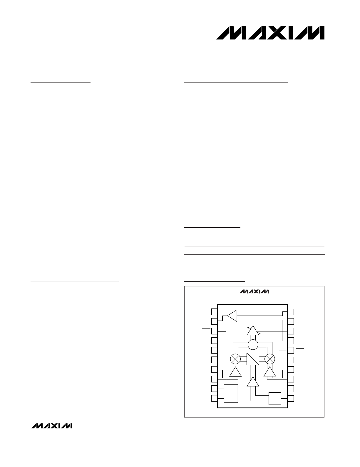
The MAX2720/MAX2721 include an I/Q modulator, a
variable gain amplifier (VGA), and a power amplifier
(PA) driver. The quadrature modulator accepts differential
baseband I/Q signals and directly modulates an RF
carrier in the 1.7GHz to 2.1GHz range (MAX2720) or
the 2.1GHz to 2.5GHz range (MAX2721). The VGA provides 35dB of output power control. The modulator’s
amplitude and phase balance yield 35dBc of sideband
suppression and 30dBc of carrier suppression. These
devices feature an LO frequency doubler that allows
the external LO source to operate at half-frequency or
full-frequency when disabled.
The MAX2720/MAX2721 operate from a single +2.7V to
+3.3V supply and require only 77mA (MAX2720) or
86mA (MAX2721) of supply current. An additional
20mA of supply current is saved by disabling the
stand-alone PA driver. A low-power shutdown mode
further reduces supply current to less than 0.1µA. The
device is packaged in the small 20-pin TSSOP-EP with
exposed paddle to improve RF performance.
Applications
Wireless Local Loop (WLL)
Wideband CDMA Systems
LMDS/MMDS
2.4GHz Broadband ISM Radios
DCS/PCS Base Stations
Features
♦ RF Frequency Range
1.7GHz to 2.1GHz (MAX2720)
2.1GHz to 2.5GHz (MAX2721)
♦ Integrated I/Q Modulator, LO Doubler, VGA, and
PA Driver
♦ 35dB VGA Gain Control Range
♦ 35dBc Sideband Suppression
♦ 30dBc Carrier Suppression
♦ Low Supply Current
77mA (MAX2720), 86mA (MAX2721)
20mA Reduction with PA Driver Disabled
♦ 0.1µA Supply Current in Shutdown Mode
♦ +2.7V to +3.3V Single-Supply Operation
MAX2720/MAX2721
1.7GHz to 2.5GHz, Direct I/Q Modulator with
VGA and PA Driver
________________________________________________________________ Maxim Integrated Products 1
4
5
20 DRIN
19 GND
18 PC
V
CC
2DROUT
1GND
17
MODOUT
16
15 V
CC
14 Q-
7
I-
6V
CC
GND
13 Q+
12 V
CC
11 LO
9V
CC
8I+
MAX2720/MAX2721
3SHDN
ENX2
0°
90°
PA DRIVER
VGA
LO DOUBLER
LO PHASE SHIFTER
10GND
Σ
x2
BIAS
Functional Diagram
19-1606; Rev 0; 1/00
PART
MAX2720EUP
MAX2721EUP
-40°C to +85°C
-40°C to +85°C
TEMP. RANGE PIN-PACKAGE
20 TSSOP-EP*
20 TSSOP-EP*
Pin Configuration appears at end of data sheet.
*Exposed paddle.
Ordering Information
For free samples and the latest literature, visit www.maxim-ic.com or phone 1-800-998-8800.
For small orders, phone 1-800-835-8769.
MAX2720/MAX2721
1.7GHz to 2.5GHz, Direct I/Q Modulator with
VGA and PA Driver
2 _______________________________________________________________________________________
ABSOLUTE MAXIMUM RATINGS
DC ELECTRICAL CHARACTERISTICS
(VCC= +2.7V to +3.3V; SHDN = VCC; ENX2 = GND; VPC= 0.5V; no input AC signals applied to I+, I-, Q+, Q-, LO, DRIN. MODOUT
and DROUT = V
CC, TA
= -40°C to +85°C. Typical values are at V
CC.
= +3V, TA= +25°C, unless otherwise noted.)
AC ELECTRICAL CHARACTERISTICS
(MAX2720/MAX2721 EV Kit, VCC= +3.0V, SHDN = VCC, ENX2 = GND, VPC= 2.5V, input I/Q signals driven in quadrature, from a
1kΩ source impedance, single-ended, f
I+
= fQ+= 500kHz, VI+= VQ+= 200mVp-p, PLO= -13dBm, fLO= 950MHz (MAX2720), fLO=
1157.5MHz (MAX2721), P
DRIN
= -12dBm, f
DRIN
= 1900MHz (MAX2720), f
DRIN
= 2315MHz (MAX2721), MODOUT and DROUT ports
are matched to a 50Ω load, T
A
= +25°C, unless otherwise noted.) (Note 1)
Stresses beyond those listed under “Absolute Maximum Ratings” may cause permanent damage to the device. These are stress ratings only, and functional
operation of the device at these or any other conditions beyond those indicated in the operational sections of the specifications is not implied. Exposure to
absolute maximum rating conditions for extended periods may affect device reliability.
VCCto GND..............................................................-0.3V to +6V
ENX2, SHDN, PC, I+, I-, Q+, Q-, LO,
DRIN to GND........................................-0.3V to (V
CC
+ 0.3V)
ENX2, SHDN Continuous Current.....................................±10mA
PC Continuous Current.....................................................±10mA
I+ to I-, Q+ to Q- ....................................................................±2V
MODOUT, DROUT to GND Short-Circuit Duration .................10s
Continuous Power Dissipation (T
A
= +70°C)
20-Pin TSSOP-EP (derate 21.7mW/°C above +70°C) ......1.74W
Operating Temperature Range ...........................-40°C to +85°C
Junction Temperature......................................................+150°C
Storage Temperature Range ............................ -65°C to +150°C
Lead Temperature (soldering 10s) ................................. +300°C
MAX2721
MAX2720
0.5V < VPC< 2.5V, SHDN = GND
0.5V < VPC< 2.5V
MAX2720, DRIN = GND
MAX2721, DRIN = GND
SHDN = GND
CONDITIONS
86 129
mA
77 119
V
2.7 3.3
Supply Voltage
Supply Current
2.5
µA
-5 5
PC Input Bias Current
µA
-1 1
Logic Input Bias Current
V
0.5
Logic Input Low Voltage
mA
59 86
Supply Current with PA Driver
Disabled
67 96
µA
0.1 10
Shutdown Supply Current
V
2.0
Logic Input High Voltage
UNITSMIN TYP MAXPARAMETER
100kHz < fI= fQ< 2MHz
100kHz < fI+= fQ+< 2MHz
fI= fQ< BW
-1dB
fI= fQ< BW
-1dB
fI= fQ < BW
-3dB
, 0.5V < VPC< 2.5V
fI= fQ< BW
-3dB
, 0.5V < VPC< 2.5V
fI= fQ< BW
-1dB
CONDITIONS
MHz
40
I/Q Input -3dB Bandwidth (Note 2)
MHz
14 20
I/Q BASEBAND INPUTS
I/Q Input -1dB Bandwidth (Note 2)
ns
1
Group Delay Mismatch
ns
1
Group Delay Ripple
pF
5
I/Q Input Capacitance
Ω
18
I/Q Input Resistance Mismatch
mVp-p
200 630
I/Q Differential Input Level
dB
±0.2
I/Q Gain Imbalance
degrees
±1.0
I/Q Phase Imbalance
kΩ
1.6 2.0
I/Q Input Resistance
UNITSMIN TYP MAXPARAMETER
MAX2720/MAX2721
1.7GHz to 2.5GHz, Direct I/Q Modulator with
VGA and PA Driver
_______________________________________________________________________________________ 3
AC ELECTRICAL CHARACTERISTICS (continued)
(MAX2720/MAX2721 EV Kit, VCC= +3.0V, SHDN = VCC, ENX2 = GND, VPC= 2.5V, input I/Q signals driven in quadrature, from a
1kΩ source impedance, single-ended, f
I+
= fQ+= 500kHz, VI+= VQ+= 200mVp-p, PLO= -13dBm, fLO= 950MHz (MAX2720), fLO=
1157.5MHz (MAX2721), P
DRIN
= -12dBm, f
DRIN
= 1900MHz (MAX2720), f
DRIN
= 2315MHz (MAX2721), MODOUT and DROUT ports
are matched to a 50Ω load, T
A
= +25°C, unless otherwise noted.) (Note 1)
VPC= 2.5V
MAX2721
ENX2 = GND
MAX2721
MAX2720
ENX2 = V
CC
VPC= 2.5V
0.5V < VPC< 2.5V
VPC= 2.5V, I/Q terminated in 50Ω
Slope between VPC= 1V and VPC= 2V
dBm
+8 +14
MAX2721, VPC= 2.5V, ENX2 = VCCor GND,
T
A
= +25°C (Note 3)
Output Third-Order Intercept Point
(Note 4)
MAX2720
CONDITIONS
+3 +6
MAX2721
MAX2721
ENX2 = GND
30 40
ENX2 = V
CC
20 25
ENX2 = GND
ENX2 = V
CC
24 31
ENX2 = GND
ENX2 = V
CC
MAX2720, 0.5V < VPC< 2.5V
+9 +14
2:1
Output VSWR
dBm/Hz
-141 -137
Out-of-Band Noise Density
26 33
MAX2720
MAX2721
VCC= +3.0V + 100mVp-p at 10kHz/300kHz
MAX2720
0.5V < VPC< 2.5V
50 45
MODOUT to LO Input Isolation
1.8:1
1.9:1
LO Input VSWR
2100 2500
MAX2720, VPC= 2.5V, ENX2 = VCCor GND,
T
A
= +25°C (Note 3)
MHz
1700 2100
2100 2500
1050 1250
1.8:1
Frequency Range (Note 3)
dBm
+1 +5
Output 1dB Compression Point
dB/V
19 23
dBc
PC Slope
VPC= 2.5V
41
VPC= 0.5V
Power-Supply Ripple Rejection
(Note 5)
dBm
-12.5 -8.5 -6.0
Output Power, High
MAX2720
-10.5 -5.0 -2.5
MAX2721
MHz
UNITSMIN TYP MAX
850 1050
PARAMETER
LO Frequency Range (Note 3)
1700 2100
28 35
1.6:1
MODULATOR OUTPUT
dBcCarrier Suppression
Sideband Suppression dBc
dB
VPC= 2.5V,
TA= -40°C to +85°C
dB
±1.0 ±1.8
Output Power Variation Over
Temperature
±0.8 ±1.5
MAX2720
MAX2721
MAX2720
MAX2721
dBm
-16 -10
LO Input Power (Note 3)
VPC= 0.5V,
ENX2 = V
CC
or GND
dB
29 35
Power Control Range
28 32
MAX2720
MAX2721
LO BUFFER, LO FREQUENCY DOUBLER, QUADRATURE GENERATOR
MAX2720/MAX2721
1.7GHz to 2.5GHz, Direct I/Q Modulator with
VGA and PA Driver
4 _______________________________________________________________________________________
Note 1: Min/max limits are guaranteed by design and characterization and are not production tested.
Note 2: I/Q input bandwith is determined by the baseband source impedance and the I/Q input capacitance. The bandwith can be
increased by lowering the baseband source impedance.
Note 3: MODOUT output power specifications are met over this frequency range for V
PC
= 2.5V and TA= +25°C.
Note 4 IP3 measured with two tones, f
1
= 500kHz and f2= 600kHz, at 100mVp-p each.
Note 5: Measured relative to desired upconverted signal level.
Note 6 DROUT gain specifications are met over this frequency range at T
A
= +25°C.
Note 7: IP3 measured with two tones, f
1
= 1900MHz and f2= 1901MHz, at -18dBm each.
Note 8: IP3 measured with two tones, f
1
= 2315MHz and f2= 2316MHz, at -18dBm each.
CONDITIONS
MAX2720
MAX2721
MAX2720
MAX2721
UNITSMIN TYP MAXPARAMETER
MAX2720
MAX2720
MAX2721
MAX2720
MAX2721
TA= -40°C to +85°C
MHz
1700 2100
Frequency Range (Note 6)
dBm
+9.5 +12.5
Output 1dB Compression Point
2.6
dB
2.4
Noise Figure
±0.3 ±0.8
2100 2500
dB
11 13.5 15.5
Gain Variation Over Temperature
8.5 11.5 15.5
±0.4 ±0.8
MAX2721 (Note 8)
MAX2720 (Note 7)
MAX2721
dB
19
Reverse Isolation
+20 +24
dB
65
DROUT to LO Input Isolation
1.5:1
Input VSWR
1.5:1
Output VSWR
dBm
+22 +24
Output Third-Order Intercept Point
+8 +11
AC ELECTRICAL CHARACTERISTICS (continued)
(MAX2720/MAX2721 EV Kit, VCC= +3.0V, SHDN = VCC, ENX2 = GND, VPC= 2.5V, input I/Q signals driven in quadrature, from a
1kΩ source impedance, single-ended, f
I+
= fQ+= 500kHz, VI+= VQ+= 200mVp-p, PLO= -13dBm, fLO= 950MHz (MAX2720), fLO=
1157.5MHz (MAX2721), P
DRIN
= -12dBm, f
DRIN
= 1900MHz (MAX2720), f
DRIN
= 2315MHz (MAX2721), MODOUT and DROUT ports
are matched to a 50Ω load, T
A
= +25°C, unless otherwise noted.) (Note 1)
Gain (Note 6) dB
PA DRIVER
MAX2720/MAX2721
1.7GHz to 2.5GHz, Direct I/Q Modulator with
VGA and PA Driver
_______________________________________________________________________________________ 5
0
30
20
10
40
50
60
70
80
90
100
2.7 2.92.8 3.0 3.1 3.2 3.3
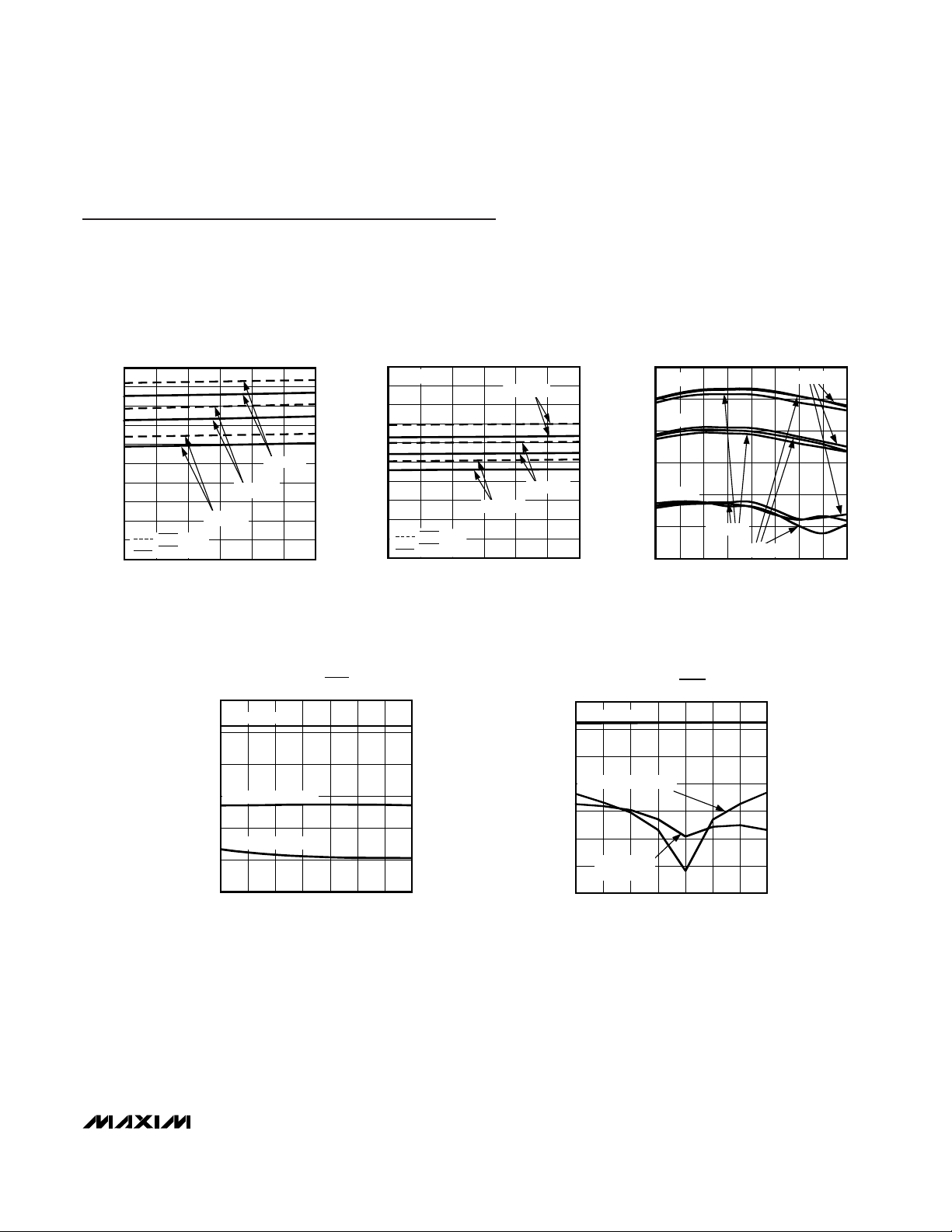
SUPPLY CURRENT vs. SUPPLY VOLTAGE
WITH PA DRIVER ENABLED
MAX2720/21toc01
SUPPLY VOLTAGE (V)
SUPPLY CURRENT (mA)
TA = +85°C
TA = +25°C
TA = -40°C
ENX2 = GND
ENX2 = V
CC
0
30
20
10
40
50
60
70
80
90
100
2.7 2.92.8 3.0 3.1 3.2 3.3
SUPPLY CURRENT vs. SUPPLY VOLTAGE
WITH PA DRIVER DISABLED
MAX2720/21toc02
SUPPLY VOLTAGE (V)
SUPPLY CURRENT (mA)
ENX2 = GND
ENX2 = V
CC
DRIN = GND
TA = +85°C
TA = +25°C
TA = -40°C
-60
-50
-40
-30
-20
-10
0
1700 1800 1900 2000 2100
MODULATOR OUTPUT POWER
vs. RF FREQUENCY
MAX2720/21toc04
RF FREQUENCY (MHz)
OUTPUT POWER (dBm)
TA = +85°C
V
PC
= 2.5V
V
PC
= 1.5V
V
PC
= 0.5V
TA = +25°C
TA = -40°C
-60
-40
-50
-20
-30
-10
0
-19 -13 -11-17 -15 -9 -7 -5
MAX2720/21toc05
LO POWER (dBm)
OUTPUT POWER (dBm) AND CARRIER
AND SIDEBAND SUPPRESSION (dBc)
OUTPUT POWER
CARRIER SUPPRESSION
SIDEBAND SUPPRESSION
MODULATOR PERFORMANCE
vs. LO POWER (ENX2 = GND)
-70
-50
-60
-20
-30
-40
-10
0
-19 -13 -11-17 -15 -9 -7 -5
MAX2720/21toc06
LO POWER (dBm)
OUTPUT POWER (dBm) AND CARRIER
AND SIDEBAND SUPPRESSION (dBc)
OUTPUT POWER
MODULATOR PERFORMANCE
vs. LO POWER (ENX2 = V
CC
)
CARRIER SUPPRESSION
SIDEBAND
SUPPRESSION
Typical Operating Characteristics
(MAX2720/MAX2721 EV Kit, VCC= +3.0V, SHDN = VCC, ENX2 = GND, VPC= 2.5V, input I/Q signals driven in quadrature, from a
1kΩ source impedance, single-ended, f
I+
= fQ+= 500kHz, VI+= VQ+= 200mVp-p, PLO= -13dBm, fLO= 950MHz (MAX2720), fLO=
1157.5MHz (MAX2721), P
DRIN
= -12dBm, f
DRIN
= 1900MHz (MAX2720), f
DRIN
= 2315MHz (MAX2721), MODOUT and DROUT ports
are matched to a 50Ω load, T
A
= +25°C, unless otherwise noted.) (Note 1)
MAX2720
MAX2720/MAX2721
1.7GHz to 2.5GHz, Direct I/Q Modulator with
VGA and PA Driver
6 _______________________________________________________________________________________
-50
-35
-40
-45
-15
-10
-20
-30
-25
-5
0
0 1.50.5 1.0 2.0 2.5 3.0
MAX2720/21toc10
PC VOLTAGE (V)
OUTPUT POWER (dBm)
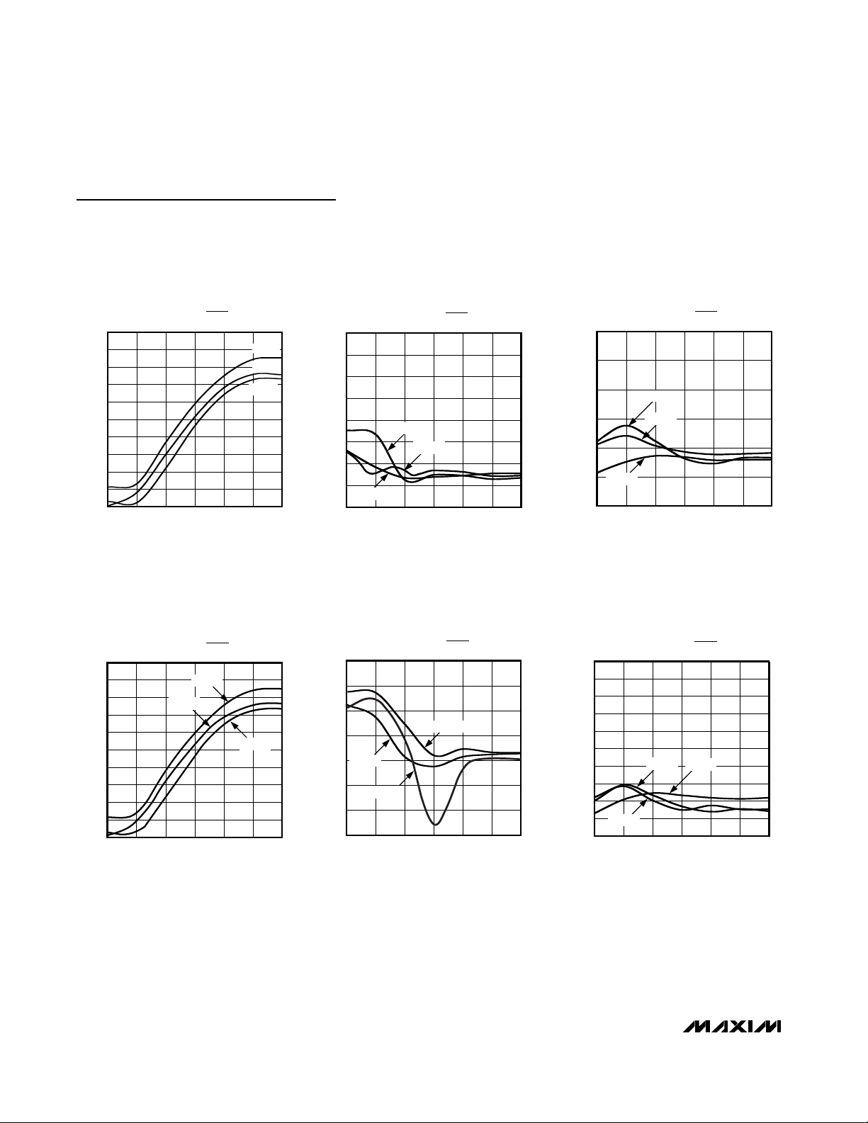
MODULATOR OUTPUT POWER
vs. PC VOLTAGE (ENX2 = V
CC
)
2.1GHz
1.9GHz
1.7GHz
-70
-50
-60
-40
-10
-20
-30
0
0 1.50.5 1.0 2.0 2.5 3.0
MAX2720/21toc11
PC VOLTAGE (V)
CARRIER SUPPRESSION (dBc)
MODULATOR CARRIER SUPPRESSION
vs. PC VOLTAGE (ENX2 = V
CC
)
2.1GHz
1.9GHz
1.7GHz
-50
-35
-40
-45
-15
-10
-20
-30
-25
-5
0
0 1.50.5 1.0 2.0 2.5 3.0
MAX2720/21toc12
PC VOLTAGE (V)
SIDEBAND SUPPRESSION (dBc)
MODULATOR SIDEBAND SUPPRESSION
vs. PC VOLTAGE (ENX2 = V
CC
)
2.1GHz
1.7GHz
1.9GHz
Typical Operating Characteristics (continued)
(MAX2720/MAX2721 EV Kit, VCC= +3.0V, SHDN = VCC, ENX2 = GND, VPC= 2.5V, input I/Q signals driven in quadrature, from a
1kΩ source impedance, single-ended, f
I+
= fQ+= 500kHz, VI+= VQ+= 200mVp-p, PLO= -13dBm, fLO= 950MHz (MAX2720), fLO=
1157.5MHz (MAX2721), P
DRIN
= -12dBm, f
DRIN
= 1900MHz (MAX2720), f
DRIN
= 2315MHz (MAX2721), MODOUT and DROUT ports
are matched to a 50Ω load, TA= +25°C, unless otherwise noted.) (Note 1)
-40
-35
-15
-10
-20
-30
-25
-5
0
0 1.50.5 1.0 2.0 2.5 3.0
MAX2720/21toc08
PC VOLTAGE (V)
CARRIER SUPPRESSION (dBc)
MODULATOR CARRIER SUPPRESSION
vs. PC VOLTAGE (ENX2 = GND)
2.1GHz
1.9GHz
1.7GHz
-60
-40
-50
-20
-30
-10
0
0 1.0 1.50.5 2.0 2.5 3.0
MAX2720/21toc09
PC VOLTAGE (V)
SIDEBAND SUPPRESSION (dBc)
MODULATION SIDEBAND SUPPRESSION
vs. PC VOLTAGE (ENX2 = GND)
2.1GHz
1.9GHz
1.7GHz
MAX2720
-50
-35
-40
-45
-15
-10
-20
-30
-25
-5
0
0 1.50.5 1.0 2.0 2.5 3.0
MAX2720/21toc07
PC VOLTAGE (V)
OUTPUT POWER (dBm)
1.9GHz
1.7GHz
2.1GHz
MODULATOR OUTPUT POWER
vs. PC VOLTAGE (ENX2 = GND)
MAX2720/MAX2721
1.7GHz to 2.5GHz, Direct I/Q Modulator with
VGA and PA Driver
_______________________________________________________________________________________ 7
Typical Operating Characteristics (continued)
(MAX2720/MAX2721 EV Kit, VCC= +3.0V, SHDN = VCC, ENX2 = GND, VPC= 2.5V, input I/Q signals driven in quadrature, from a
1kΩ source impedance, single-ended, f
I+
= fQ+= 500kHz, VI+= VQ+= 200mVp-p, PLO= -13dBm, fLO= 950MHz (MAX2720), fLO=
1157.5MHz (MAX2721), P
DRIN
= -12dBm, f
DRIN
= 1900MHz (MAX2720), f
DRIN
= 2315MHz (MAX2721), MODOUT and DROUT ports
are matched to a 50Ω load, TA= +25°C, unless otherwise noted.) (Note 1)
-35
-40
-15
-10
-20
-30
-25
-5
0
0 1.50.5 1.0 2.0 2.5 3.0
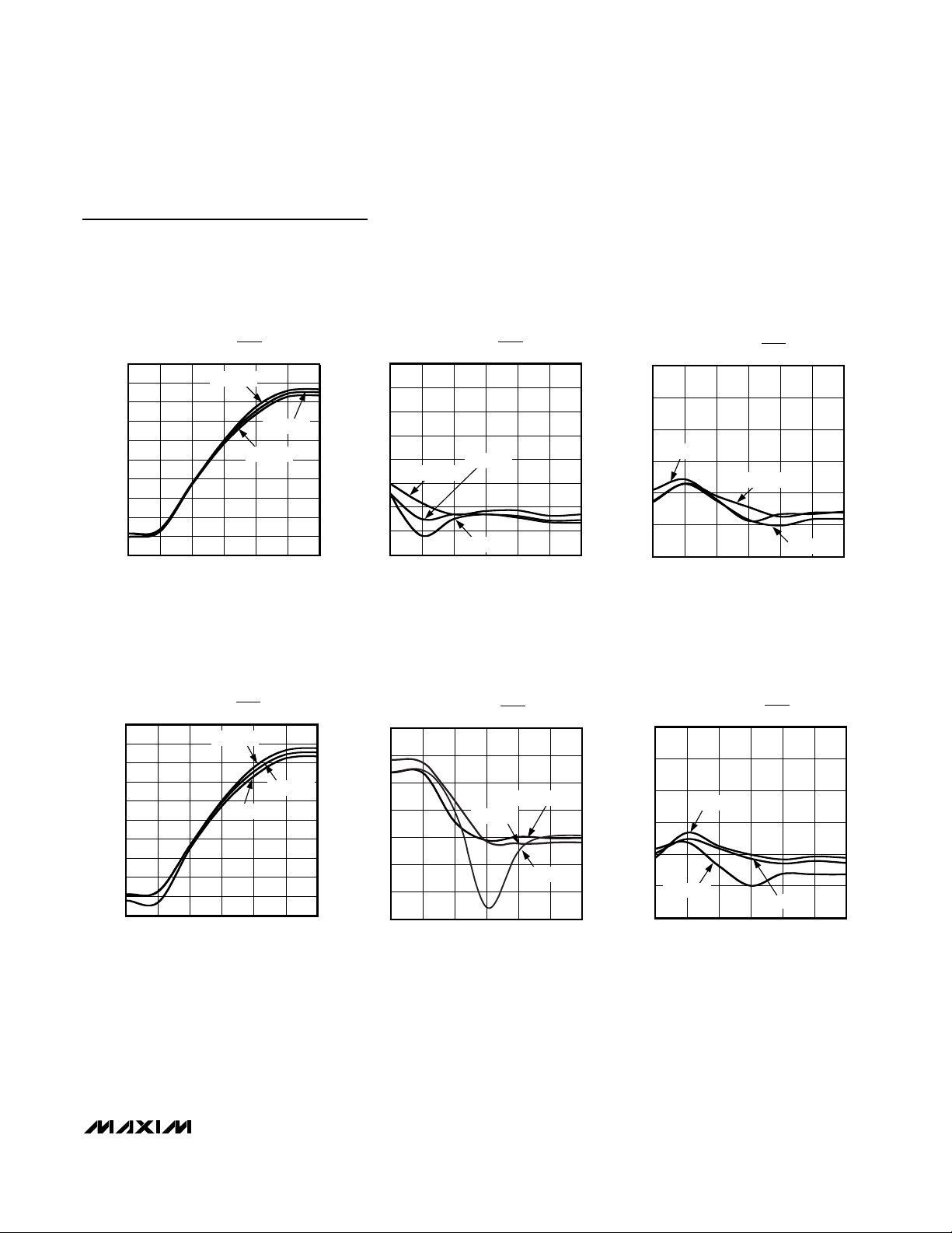
MAX2720/21toc14
PC VOLTAGE (V)
CARRIER SUPPRESSION (dBc)
MODULATOR CARRIER SUPPRESSION
vs. PC VOLTAGE (ENX2 = GND)
TA = +85°C
TA = +25°C
TA = -40°C
-55
-60
-20
-30
-40
-10
0
0 1.50.5 1.0 2.0 2.5 3.0
MAX2720/21toc15
PC VOLTAGE (V)
SIDEBAND SUPPRESSION (dBc)
MODULATOR SIDEBAND SUPPRESSION
vs. PC VOLTAGE (ENX2 = GND)
TA = +85°C
TA = +25°C
TA = -40°C
-45
-40
-50
-15
-20
-25
-35
-30
-5
-10
0
0 1.50.5 1.0 2.0 2.5 3.0
MAX2720/21toc16
PC VOLTAGE (V)
OUTPUT POWER (dBm)
MODULATOR OUTPUT POWER
vs. PC VOLTAGE (ENX2 = V
CC
)
TA = +85°C
TA = +25°C
TA = -40°C
-40
-70
-50
-60
-20
-30
-10
0
0 1.50.5 1.0 2.0 2.5 3.0
MAX2720/21toc17
PC VOLTAGE (V)
CARRIER SUPRESSION (dBc)
MODULATOR CARRIER SUPPRESSION
vs. PC VOLTAGE (ENX2 = V
CC
)
TA = +85°C
TA = +25°C
TA = -40°C
-40
-50
-60
-20
-30
-10
0
0 1.50.5 1.0 2.0 2.5 3.0
MAX2720/21toc18
SIDEBAND SUPRESSION (dBc)
TA = +85°C
TA = -40°C
MODULATOR SIDEBAND SUPPRESSION
vs. PC VOLTAGE (ENX2 = V
CC
)
TA = +25°C
MAX2720
-50
-35
-40
-45
-15
-10
-20
-30
-25
-5
0
0 1.50.5 1.0 2.0 2.5 3.0
MAX2720/21toc13
PC VOLTAGE (V)
OUTPUT POWER (dBm)
TA = +85°C
TA = +25°C
TA = -40°C
MODULATOR OUTPUT POWER
vs. PC VOLTAGE (ENX2 = GND)
MAX2720/MAX2721
1.7GHz to 2.5GHz, Direct I/Q Modulator with
VGA and PA Driver
8 _______________________________________________________________________________________
-60
10 10,0001000100
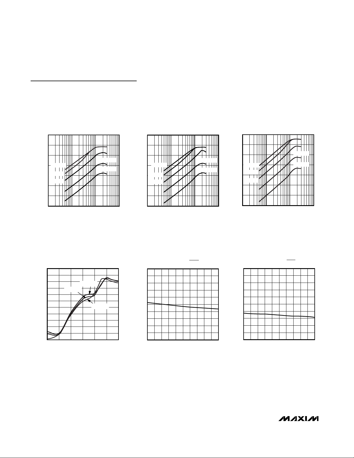
MODULATOR OUTPUT POWER
vs. INPUT LEVEL (T
A
= +25°C)
10
-30
-40
-50
0
-10
-20
MAX2720 toc20
INPUT LEVEL (mVp-p)
OUTPUT POWER (dBm)
VPC = 2.5V
VPC = 2.0V
VPC = 1.5V
VPC = 1.0V
VPC = 0.5V
-60
10 10,0001000100
MODULATOR OUTPUT POWER
vs. INPUT LEVEL (T
A
= +85°C)
10
-30
-40
-50
0
-10
-20
MAX2720 toc21
INPUT LEVEL (mVp-p)
OUTPUT POWER (dBm)
VPC = 2.5V
VPC = 2.0V
VPC = 1.5V
VPC = 1.0V
VPC = 0.5V
-20
-15
-30
-25
15
10
0
-5
-10
5
20
25
1.00 0.5 1.5 2.0 2.5 3.0
MODULATOR OUTPUT IP3
vs. PC VOLTAGE
MAX2720/21toc22
PC VOLTAGE (V)
OUTPUT IP3 (dBm)
TA = +25°C
TA = -40°C
TA = +85°C
1.0
1.2
1.6
2.0
2.4
2.8
850 890 930 970 1010 1050
MAX2720-24
FREQUENCY (MHz)
VSWR
LO PORT VSWR
vs. LO FREQUENCY (ENX2 = GND)
1.0
1.4
1.8
2.0
2.4
2.8
1700 1780 1860 1940 2020 2100
MAX2720-25
FREQUENCY (MHz)
VSWR
LO PORT VSWR
vs. LO FREQUENCY (ENX2 = V
CC
)
Typical Operating Characteristics (continued)
(MAX2720/MAX2721 EV Kit, VCC= +3.0V, SHDN = VCC, ENX2 = GND, VPC= 2.5V, input I/Q signals driven in quadrature, from a
1kΩ source impedance, single-ended, f
I+
= fQ+= 500kHz, VI+= VQ+= 200mVp-p, PLO= -13dBm, fLO= 950MHz (MAX2720), fLO=
1157.5MHz (MAX2721), P
DRIN
= -12dBm, f
DRIN
= 1900MHz (MAX2720), f
DRIN
= 2315MHz (MAX2721), MODOUT and DROUT ports
are matched to a 50Ω load, TA= +25°C, unless otherwise noted.) (Note 1)
MAX2720
-60
10 10,0001000100
MODULATOR OUTPUT POWER
vs. INPUT LEVEL (T
A
= -40°C)
10
-30
-40
-50
0
-10
-20
MAX2720 toc19
INPUT LEVEL (mVp-p)
OUTPUT POWER (dBm)
VPC = 2.5V
VPC = 2.0V
VPC = 1.5V
VPC = 1.0V
VPC = 0.5V

MAX2720/MAX2721
1.7GHz to 2.5GHz, Direct I/Q Modulator with
VGA and PA Driver
_______________________________________________________________________________________ 9
10
11
12
13
14
15
2.7 2.92.8 3.0 3.1 3.2 3.3
PA DRIVER GAIN vs.
SUPPLY VOLTAGE
MAX2720/21toc27
SUPPLY VOLTAGE (V)
GAIN (dB)
TA = +85°C
TA = +25°C
TA = -40°C
20
22
21
23
24
26
25
28
27
29
30
2.7 2.92.8 3.0 3.1 3.2 3.3
PA DRIVER OUTPUT IP3
vs. SUPPLY VOLTAGE
MAX2720/21toc28
SUPPLY VOLTAGE (V)
OUTPUT IP3 (dBm)
TA = +85°C
TA = +25°C
TA = -40°C
10
12
11
13
14
16
15
18
17
19
20
2.7 2.92.8 3.0 3.1 3.2 3.3
PA DRIVER OUTPUT P1dB
vs. SUPPLY VOLTAGE
MAX2720/21toc29
SUPPLY VOLTAGE (V)
OUTPUT P1dB (dBm)
TA = +85°C
TA = +25°C
TA = -40°C
0
4
2
6
8
12
10
16
14
18
20
1700 1800 1900 2000 2100
PA DRIVER GAIN
vs. RF FREQUENCY
MAX2720/21toc30
RF FREQUENCY (MHz)
GAIN (dB)
TA = +25°C
TA = +85°C
TA = -40°C
Typical Operating Characteristics (continued)
(MAX2720/MAX2721 EV Kit, VCC= +3.0V, SHDN = VCC, ENX2 = GND, VPC= 2.5V, input I/Q signals driven in quadrature, from a
1kΩ source impedance, single-ended, f
I+
= fQ+= 500kHz, VI+= VQ+= 200mVp-p, PLO= -13dBm, fLO= 950MHz (MAX2720), fLO=
1157.5MHz (MAX2721), P
DRIN
= -12dBm, f
DRIN
= 1900MHz (MAX2720), f
DRIN
= 2315MHz (MAX2721), MODOUT and DROUT ports
are matched to a 50Ω load, TA= +25°C, unless otherwise noted.) (Note 1)
20
22
21
23
24
26
25
28
27
29
30
1700 1800 1900 2000 2100
PA DRIVER OUTPUT IP3
vs. FREQUENCY
MAX2720/21toc31
FREQUENCY (MHz)
OUTPUT IP3 (dBm)
TA = +25°C
TA = +85°C
TA = -40°C
10
12
11
13
14
16
15
18
17
19
20
1700 1800 1900 2000 2100
PA DRIVER OUTPUT P1dB COMPRESSION
POINT vs. FREQUENCY
MAX2720/21toc32
FREQUENCY (MHz)
OUTPUT P1dB (dBm)
TA = +25°C
TA = -40°C
TA = +85°C
MAX2720

MAX2720/MAX2721
1.7GHz to 2.5GHz, Direct I/Q Modulator with
VGA and PA Driver
10 ______________________________________________________________________________________
Typical Operating Characteristics (continued)
(MAX2720/MAX2721 EV Kit, VCC= +3.0V, SHDN = VCC, ENX2 = GND, VPC= 2.5V, input I/Q signals driven in quadrature, from a
1kΩ source impedance, single-ended, f
I+
= fQ+= 500kHz, VI+= VQ+= 200mVp-p, PLO= -13dBm, fLO= 950MHz (MAX2720), fLO=
1157.5MHz (MAX2721), P
DRIN
= -12dBm, f
DRIN
= 1900MHz (MAX2720), f
DRIN
= 2315MHz (MAX2721), MODOUT and DROUT ports
are matched to a 50Ω load, TA= +25°C, unless otherwise noted.) (Note 1)
0
1.0
0.5
1.5
2.0
3.0
2.5
4.0
3.5
4.5
5.0
1700 1800 1900 2000 2100
PA DRIVER NOISE FIGURE
vs. FREQUENCY
MAX2720/21toc33
FREQUENCY (MHz)
NOISE FIGURE (dB)
TA = +25°C
TA = +85°C
TA = -40°C
-15
-10
-5
10
5
0
15
20
-25 -15 -10-20 -5 50102015
PA DRIVER OUTPUT POWER
vs. INPUT POWER
MAX2720/21toc34
INPUT POWER (dBm)
OUTPUT POWER (dBm)
TA = -40°C
TA = +85°C
TA = +25°C
MAX2720

MAX2720/MAX2721
1.7GHz to 2.5GHz, Direct I/Q Modulator with
VGA and PA Driver
______________________________________________________________________________________ 11
-50
-40
-45
-30
-35
-20
-25
-15
-5
-10
0
2100 2200 2300 2400 2500
MODULATOR OUTPUT POWER
vs. RF FREQUENCY
MAX2720 toc38
RF FREQUENCY (MHz)
OUTPUT POWER (dBm)
VPC = 2.5V
VPC = 1.5V
VPC = 0.5V
TA= +85°C
TA= +25°C
TA= -40°C
-40
-30
-35
-25
-20
-5
-15
-10
0
-19 -17 -15 -13 -11 -9 -7 -5
MODULATOR PERFORMANCE
vs. LO POWER (ENX2 = GND)
MAX2720/21toc39
RF FREQUENCY (MHz)
OUTPUT POWER (dBm) AND CARRIER AND
SIDEBAND SUPPRESSION (dBc)
OUTPUT POWER
CARRIER SUPPRESSION
SIDEBAND SUPPRESSION
-40
-30
-35
-25
-20
-15
-5
-10
0
-19 -17 -15 -13 -9 -7-11 -5
MODULATOR PERFORMANCE
vs. LO POWER (ENX2 = V
CC
)
MAX2720/21toc40
LO POWER (dBm)
OUTPUT POWER (dBm) AND CARRIER AND
SIDEBAND SUPPRESSION (dBc)
OUTPUT POWER
CARRIER SUPPRESSION
SIDEBAND SUPPRESSION
20
30
50
40
70
60
110
100
90
80
120
2.7 2.92.8 3.0 3.1 3.2 3.3
SUPPLY CURRENT vs. SUPPLY VOLTAGE
WITH PA DRIVER ENABLED
MAX2720/21toc35
SUPPLY VOLTAGE (V)
SUPPLY CURRENT (mA)
TA = +85°C
TA = +25°C
TA = -40°C
ENX2 = GND
ENX2 = V
CC
20
40
30
60
50
100
90
80
70
120
110
2.7 2.92.8 3.0 3.1 3.2 3.3
SUPPLY CURRENT vs. SUPPLY VOLTAGE
WITH PA DRIVER DISABLED
MAX2720/21toc36
SUPPLY VOLTAGE (V)
SUPPLY CURRENT (mA)
TA = +25°C
TA = -40°C
TA = +85°C
DRIN = GND
ENX2 = GND
ENX2 = V
CC
Typical Operating Characteristics (continued)
(MAX2720/MAX2721 EV Kit, VCC= +3.0V, SHDN = VCC, ENX2 = GND, VPC= 2.5V, input I/Q signals driven in quadrature, from a
1kΩ source impedance, single-ended, f
I+
= fQ+= 500kHz, VI+= VQ+= 200mVp-p, PLO= -13dBm, fLO= 950MHz (MAX2720), fLO=
1157.5MHz (MAX2721), P
DRIN
= -12dBm, f
DRIN
= 1900MHz (MAX2720), f
DRIN
= 2315MHz (MAX2721), MODOUT and DROUT ports
are matched to a 50Ω load, TA= +25°C, unless otherwise noted.) (Note 1)
MAX2721

MAX2720/MAX2721
1.7GHz to 2.5GHz, Direct I/Q Modulator with
VGA and PA Driver
12 ______________________________________________________________________________________
Typical Operating Characteristics (continued)
(MAX2720/MAX2721 EV Kit, VCC= +3.0V, SHDN = VCC, ENX2 = GND, VPC= 2.5V, input I/Q signals driven in quadrature, from a
1kΩ source impedance, single-ended, f
I+
= fQ+= 500kHz, VI+= VQ+= 200mVp-p, PLO= -13dBm, fLO= 950MHz (MAX2720), fLO=
1157.5MHz (MAX2721), P
DRIN
= -12dBm, f
DRIN
= 1900MHz (MAX2720), f
DRIN
= 2315MHz (MAX2721), MODOUT and DROUT ports
are matched to a 50Ω load, TA= +25°C, unless otherwise noted.) (Note 1)
-40
-35
-30
-25
-20
-15
-10
-5
0
0 1.00.5 1.5 2.0 2.5 3.0
MODULATOR SIDEBAND SUPRESSION
vs. PC VOLTAGE (ENX2 = V
CC
)
MAX2721 TOC46
PC VOLTAGE (V)
SIDEBAND SUPRESSION (dBc)
2.1GHz
2.5GHz
2.3GHz
-45
-35
-40
-20
-25
-30
-5
-10
-15
0
0 1.00.5 1.5 2.0 2.5 3.0
MODULATOR OUTPUT POWER
vs. PC VOLTAGE (ENX2 = V
CC
)
MAX2721 TOC44
PC VOLTAGE (V)
OUTPUT POWER (dBm)
2.1
GHz
2.3
GHz
2.5
GHz
-45
-35
-40
-20
-25
-30
-5
-10
-15
0
0 1.00.5 1.5 2.0 2.5 3.0
MODULATOR CARRIER SUPRESSION
vs. PC VOLTAGE (ENX2 = V
CC
)
MAX2721 TOC45
PC VOLTAGE (V)
CARRIER SUPRESSION (dBc)
2.1GHz
2.3GHz
2.5GHz
-40
-30
-35
-25
-20
-15
-5
-10
0
0 0.5 1.0 2.0 2.51.5
3.0
MAX2720/21toc42
PC VOLTAGE (V)
CARRIER SUPPRESSION (dBm)
CARRIER SUPPRESSION vs. PC VOLTAGE
(ENX2 = GND)
2.5GHz
2.1GHz
2.3GHz
-40
-35
-30
-25
-20
-15
-10
-5
0
0 1.00.5 1.5 2.0 2.5 3.0
SIDEBAND SUPRESSION vs. PC VOLTAGE
(ENX2 = GND)
MAX2721 TOC43
PC VOLTAGE (V)
SIDEBAND SUPRESSION (dBc)
2.3GHz
2.1GHz
2.5GHz
MAX2721
-40
-30
-35
-25
-20
-15
-5
-10
0
0 0.5 1.0 1.5 2.0 3.02.5
MAX2720/21toc41
PC VOLTAGE (V)
OUTPUT POWER (dBm)
MODULATOR OUTPUT POWER
vs. PC VOLTAGE (ENX2 = GND)
2.3GHz
2.1GHz
2.5GHz

MAX2720/MAX2721
1.7GHz to 2.5GHz, Direct I/Q Modulator with
VGA and PA Driver
______________________________________________________________________________________ 13
Typical Operating Characteristics (continued)
(MAX2720/MAX2721 EV Kit, VCC= +3.0V, SHDN = VCC, ENX2 = GND, VPC= 2.5V, input I/Q signals driven in quadrature, from a
1kΩ source impedance, single-ended, f
I+
= fQ+= 500kHz, VI+= VQ+= 200mVp-p, PLO= -13dBm, fLO= 950MHz (MAX2720), fLO=
1157.5MHz (MAX2721), P
DRIN
= -12dBm, f
DRIN
= 1900MHz (MAX2720), f
DRIN
= 2315MHz (MAX2721), MODOUT and DROUT ports
are matched to a 50Ω load, TA= +25°C, unless otherwise noted.) (Note 1)
-40
-35
-30
-25
-20
-15
-10
-5
0
0 1.00.5 1.5 2.0 2.5 3.0
MODULATOR OUTPUT POWER
vs. PC VOLTAGE (ENX2 = GND)
MAX2721 TOC47
PC VOLTAGE (V)
OUTPUT POWER (dBm)
TA = +25°C
TA = -40°C
TA = +85°C
-35
-25
-30
-15
-20
-5
-10
0
0 1.0 1.50.5 2.0 2.5 3.0
MODULATOR CARRIER SUPRESSION
vs. PC VOLTAGE (ENX2 = GND)
MAX2721 TOC48
PC VOLTAGE (V)
CARRIER SUPRESSION (dBc)
TA = +85°C
TA = +25°C
TA = -40°C
-40
-35
-30
-25
-20
-15
-10
-5
0
0 1.00.5 1.5 2.0 2.5 3.0
MODULATOR SIDEBAND SUPRESSION
vs. PC VOLTAGE (ENX2 = GND)
MAX2721 TOC49
PC VOLTAGE (V)
SIDEBAND SUPRESSION (dBc)
TA = -40°C
TA = +25°C
TA = +85°C
-40
-35
-30
-25
-20
-15
-10
-5
0
0 1.00.5 1.5 2.0 2.5 3.0
MODULATOR OUTPUT POWER
vs. PC VOLTAGE (ENX2 = V
CC
)
MAX2721 TOC450
PC VOLTAGE (V)
OUTPUT POWER (dBm)
TA = -40°C
TA = +85°C
TA = +25°C
-40
-35
-30
-25
-20
-15
-10
-5
0
0 1.00.5 1.5 2.0 2.5 3.0
MODULATOR CARRIER SUPRESSION
vs. PC VOLTAGE (ENX2) = V
CC
MAX2721 TOC51
PC VOLTAGE (V)
CARRIER SUPPRESSION (dBc)
TA = -40°C
TA = +25°C
TA = +85°C
-40
-35
-30
-25
-20
-15
-10
-5
0
0 1.00.5 1.5 2.0 2.5 3.0
MODULATOR SIDEBAND SUPPRESSION
vs. PC VOLTAGE (ENX2 = V
CC
)
MAX2721 TOC52
PC VOLTAGE (V)
SIDEBAND SUPPRESSION (dBc)
TA = -40°C
TA = +85°C
TA = +25°C
MAX2721

MAX2720/MAX2721
1.7GHz to 2.5GHz, Direct I/Q Modulator with
VGA and PA Driver
14 ______________________________________________________________________________________
-60
-50
-40
-30
-20
-10
0
10
20
10 1000100 10,000
MODULATOR OUTPUT POWER
vs. INPUT LEVEL (T
A
= +85°C)
MAX2721 TOC55
INPUT LEVEL (mVp-p)
OUTPUT POWER (dBm)
VPC = 2.5V
VPC = 1.5V
VPC = 2.0V
VPC = 1.0V
VPC = 0.5V
-30
-25
-20
-15
-10
-5
0
5
10
15
20
25
0 0.5 1.0 1.5 2.0 2.5 3.0
MODULATOR OUTPUT IP3
vs. PC VOLTAGE
MAX2721 TOC56
INPUT LEVEL (mVp-p)
OUTPUT IP3 (dBm)
TA = -40°C
TA = +85°C
TA = +25°C
-20
-15
-10
-25
15
10
-5
0
5
20
25
1.50.5 1.0 2.0 2.5
MODULATOR OUTPUT P1dB
COMPRESSION POINT vs. PC VOLTAGE
MAX2720/21toc57
PC VOLTAGE (V)
OUTPUT P1dB (dBm)
TA = +85°C
TA = +25°C
TA = -40°C
1.0
1.4
1.8
2.0
2.4
2.6
MAX2721toc58
2100 2180 2260 2340 2420 2500
LO PORT VSWR vs. LO FREQUENCY
(ENX2 = V
CC
)
FREQUENCY (MHz)
VSWR
-60
-50
-40
-30
-20
-10
0
10
20
10 1000100 10,000
MODULATOR OUTPUT POWER
vs. INPUT LEVEL (T
A
= +25°C)
MAX2721 TOC54
INPUT LEVEL (mVp-p)
OUTPUT POWER (dBm)
VPC = 2.5V
VPC = 1.5V
VPC = 2.0V
VPC = 1.0V
VPC = 0.5V
Typical Operating Characteristics (continued)
(MAX2720/MAX2721 EV Kit, VCC= +3.0V, SHDN = VCC, ENX2 = GND, VPC= 2.5V, input I/Q signals driven in quadrature, from a
1kΩ source impedance, single-ended, f
I+
= fQ+= 500kHz, VI+= VQ+= 200mVp-p, PLO= -13dBm, fLO= 950MHz (MAX2720), fLO=
1157.5MHz (MAX2721), P
DRIN
= -12dBm, f
DRIN
= 1900MHz (MAX2720), f
DRIN
= 2315MHz (MAX2721), MODOUT and DROUT ports
are matched to a 50Ω load, TA= +25°C, unless otherwise noted.) (Note 1)
MAX2721
-60
-50
-40
-30
-20
-10
0
10
20
10 1000100 10,000
MODULATOR OUTPUT POWER
vs. INPUT LEVEL (T
A
= -40°C)
MAX2721 TOC53
INPUT LEVEL (mVp-p)
OUTPUT POWER (dBm)
VPC = 2.5V
VPC = 1.5V
VPC = 2.0V
VPC = 1.0V
VPC = 0.5V

MAX2720/MAX2721
1.7GHz to 2.5GHz, Direct I/Q Modulator with
VGA and PA Driver
______________________________________________________________________________________ 15
8
10
9
11
12
14
13
16
15
17
18
2.7 2.92.8 3.0 3.1 3.2 3.3
PA DRIVER OUTPUT P1dB
vs. SUPPLY VOLTAGE
MAX2720/21toc63
SUPPLY VOLTAGE (V)
OUTPUT P1dB (dBm)
TA = +85°C
TA = +25°C
TA = -40°C
1.0
1.4
1.6
1.8
2.0
MAX2721toc59
LO PORT VSWR vs. FREQUENCY
(ENX2 = GND)
1050 1090 1130 1170
FREQUENCY (MHz)
1210 1250
VSWR
10
11
13
12
14
15
2.7 2.92.8 3.0 3.1 3.2 3.3
PA DRIVER GAIN vs. SUPPLY VOLTAGE
MAX2721 TOC61
SUPPLY VOLTAGE (V)
GAIN (dB)
TA = +25°C
TA = -40°C
TA = +85°C
-2
2
0
4
6
10
8
14
12
16
18
2100 2200 2300 2400 2500
PA DRIVER GAIN
vs. RF FREQUENCY
MAX2720/21toc64
RF FREQUENCY (MHz)
GAIN (dB)
TA = +25°C
TA = +85°C
TA = -40°C
20
22
21
23
24
26
25
28
27
29
30
2.7 2.92.8 3.0 3.1 3.2 3.3
PA DRIVER OUTPUT IP3
vs. SUPPLY VOLTAGE
MAX2720/21toc62
SUPPLY VOLTAGE (V)
OUTPUT IP3 (dBm)
TA = +85°C
TA = -40°C
TA = +25°C
Typical Operating Characteristics (continued)
(MAX2720/MAX2721 EV Kit, VCC= +3.0V, SHDN = VCC, ENX2 = GND, VPC= 2.5V, input I/Q signals driven in quadrature, from a
1kΩ source impedance, single-ended, f
I+
= fQ+= 500kHz, VI+= VQ+= 200mVp-p, PLO= -13dBm, fLO= 950MHz (MAX2720), fLO=
1157.5MHz (MAX2721), P
DRIN
= -12dBm, f
DRIN
= 1900MHz (MAX2720), f
DRIN
= 2315MHz (MAX2721), MODOUT and DROUT ports
are matched to a 50Ω load, TA= +25°C, unless otherwise noted.) (Note 1)
20
22
21
23
24
26
25
28
27
29
2100 2200 2300 2400 2500
PA DRIVER OUTPUT IP3
vs. FREQUENCY
MAX2720/21toc65
FREQUENCY (MHz)
OUTPUT IP3 (dBm)
TA = +85°C
TA = +25°C
TA = -40°C
MAX2721

MAX2720/MAX2721
1.7GHz to 2.5GHz, Direct I/Q Modulator with
VGA and PA Driver
16 ______________________________________________________________________________________
0
2
1
3
4
6
5
8
7
9
10
2100 2200 2300 2400 2500
PA DRIVER NOISE FIGURE
vs. FREQUENCY
MAX2720/21toc67
FREQUENCY (MHz)
NOISE FIGURE (dB)
TA = +25°C
TA = -40°C
TA = +85°C
-15
-10
5
10
15
2.0
-25 -15 -10-20 -5 -50102015
PA DRIVER OUTPUT POWER
vs. INPUT POWER
MAX2720/21toc68
INPUT POWER (dBm)
OUTPUT POWER (dBm)
TA = -40°C
TA = +85°C
TA = +25°C
Typical Operating Characteristics (continued)
(MAX2720/MAX2721 EV Kit, VCC= +3.0V, SHDN = VCC, ENX2 = GND, VPC= 2.5V, input I/Q signals driven in quadrature, from a
1kΩ source impedance, single-ended, f
I+
= fQ+= 500kHz, VI+= VQ+= 200mVp-p, PLO= -13dBm, fLO= 950MHz (MAX2720), fLO=
1157.5MHz (MAX2721), P
DRIN
= -12dBm, f
DRIN
= 1900MHz (MAX2720), f
DRIN
= 2315MHz (MAX2721), MODOUT and DROUT ports
are matched to a 50Ω load, TA= +25°C, unless otherwise noted.) (Note 1)
MAX2721
0
4
2
6
8
12
10
16
14
18
20
2100 2200 2300 2400 2500
PA DRIVER OUTPUT P1dB
vs. FREQUENCY
MAX2720/21toc66
FREQUENCY (MHz)
OUTPUT P1dB (dBm)
TA = +25°C
TA = +85°C
TA = -40°C

MAX2720/MAX2721
1.7GHz to 2.5GHz, Direct I/Q Modulator with
VGA and PA Driver
______________________________________________________________________________________ 17
Detailed Description
The MAX2720/MAX2721 upconvert in-phase (I) and
quadrature (Q) baseband signals directly to RF
frequencies of 1700MHz to 2100MHz (MAX2720) or
2100MHz to 2500MHz (MAX2721). They are designed
for wideband-CDMA and WLL systems where direct I/Q
modulation of the RF carrier reduces system cost, component count, and board space compared to
dual-conversion architectures.
Internally, the MAX2720/MAX2721 include an I/Q modulator, a variable gain amplifier (VGA), and a PA driver.
Separate modulator output and PA driver input ports
allow insertion of a bandpass filter between the modulator
and PA driver for increased noise rejection. Disable the
stand-alone PA driver to reduce current consumption.
A low-power shutdown mode further reduces current
consumption to less than 0.1µA. Additionally, a logiclevel control disables or enables an internal frequency
doubler that allows the external LO to run at full or half
frequency.
NAME FUNCTION
1, 5, 10, 19, EP GND
Ground. Connect to ground plane with lowest inductance path. Solder exposed paddle
evenly to the board ground plane.
2 DROUT
PA Driver Open-Collector Output Port. Requires an external matching network and a pullup inductor to VCCfor proper biasing. See Typical Application Circuit for recommended
component values.
PIN
3
SHDN
Shutdown Control Input. Drive with a logic-level high to enable the device. Drive with a logiclevel low to disable the device. Bypass with a 1000pF capacitor to ground, as close to the
pin as possible to minimize the amount of external noise coupled onto the control line.
4, 6, 9, 12, 15 V
CC
Supply Voltage Input. Bypass to ground with the specified capacitor as close to the pin as
possible. (See Typical Application Circuit.)
16
ENX2
Logic-Level Enable Input for LO Doubler. Drive with a logic-level low to enable the doubler,
allowing the external LO to run at half-frequency, fLO= f
OUT
/ 2. Drive with a logic-level
high to disable the doubler, and allow the external LO to run at full-frequency, f
LO
= f
OUT
.
Bypass with a 1000pF capacitor to ground as close to the pin as possible to minimize
noise coupled into the control line.
13, 14 Q+, Q-
Quadrature Differential Input Ports. Requires DC-blocking capacitors. See Typical Application
Circuit for recommended component values.
11 LO
Local Oscillator input. Internally matched to 50Ω over the operating frequency band.
Requires a DC-blocking capacitor. See Typical Application Circuit for recommended component values.
7, 8 I-, I+
In-Phase Differential Input Ports. Requires DC-blocking capacitors. See Typical Application
Circuit for recommended component values.
20 DRIN
PA Driver Amplifier Input Port. Requires an external matching network and a DC-blocking
capacitor that can be part of the matching network. See Typical Application Circuit for recommended component values. Connect to ground to disable the PA Driver and reduce
supply current.
18 PC
Modulator Power Control Input. Apply a voltage between 0.5V to 2.5V to vary the output
power of the I/Q modulator over a 30dB range. Bypass with a 1000pF capacitor to ground
as close to the pin as possible to minimize noise on the control line.
17 MODOUT
Modulator Open-Collector Output Port. Requires an external matching network and a pullup inductor to VCCfor proper biasing. See Typical Application Circuit for recommended
component values.
Pin Description

MAX2720/MAX2721
1.7GHz to 2.5GHz, Direct I/Q Modulator with
VGA and PA Driver
18 ______________________________________________________________________________________
I/Q Modulator
The MAX2720/MAX2721 modulator is composed of a pair
of matched double-balanced mixers, an active LO quadrature generator, and a summing amplifier. The pair of
mixers accept differential I/Q baseband signals that
directly modulate the internal 0° and 90° LO signals
applied to the I/Q mixers. An external LO source drives
an internal LO quadrature generator that shifts the phase
of the LO signal applied to the Q mixer by 90° relative to
the LO signal applied to the I channel mixer. The modulated output of the I/Q mixers is summed together, and
the undesired sideband is suppressed.
The I+, I-, Q+, and Q- input ports feature high-linearity
buffer amplifiers with a -1dB bandwidth of 20MHz and
a -3dB bandwidth of 38MHz (1kΩ I/Q source impedance), and accept differential input voltages up to
630mVp-p. Input bandwith can be extended to beyond
100MHz by lowering the I/Q source impedance. The
ports are internally biased and therefore require DCblocking capacitors. For single-ended operation,
bypass the I- and Q- ports with a capacitor to ground
equal in value to the DC-blocking capacitors used on
the I+ and Q+ ports. See the Typical Application Circuit
for recommended component values.
Variable Gain Amplifier (VGA)
A VGA follows the summing amplifier of the I/Q modulator.
Apply a voltage between 0.5V and 2.5V to PC to vary
the output power of the modulator over a 32dB span.
The open-collector MODOUT output requires a pull-up
inductor to VCCfor proper biasing, an external matching
network for optimum power transfer, and a DC-blocking
capacitor. Since the MAX2720/MAX2721 are optimized
for different frequency ranges, they require different
output matching networks. See the MAX2720 and
MAX2721 Typical Application Circuit for recommended
component values. See Table 1 for matching to other
frequencies.
LO Buffer and LO Frequency Doubler
The MAX2720/MAX2721 feature an internal LO frequency
doubler that allows the external LO source to run at full or
half frequency (Table 2). Operating the LO at half frequency reduces injection-pulling of the voltage-controlled oscillator (VCO) from the PA, and reduces the
complexity of designing a high-frequency VCO. An
internal two-pole bandpass filter is integrated before
the LO phase-shift network to help reduce LO harmonic
content and spurious mixing.
To enable the LO frequency doubler, drive ENX2 to a
logic-level low and operate the external LO source at
half the RF carrier frequency. To disable the LO
frequency doubler, drive ENX2 to a logic-level high and
run the external LO source at the RF carrier frequency.
See Table 2 for LO input frequency ranges.
The LO port is a single-ended input that achieves a
VSWR of better than 2:1 over the specified LO input
frequency range. Since the port is internally terminated
with 50Ω, it requires a DC-blocking capacitor. See the
Typical Applications Circuits for recommended component values. For optimum performance, drive the LO
port with an input power of -16dBm to -10dBm. Driving
the LO port with lower input power levels may affect
quadrature performance, while higher input powers
may increase LO leakage.
PA Driver Amplifier
The PA driver provides a gain of 13.5dB for the
MAX2720 and 11.5dB for the MAX2721. The DRIN
input port requires an external matching network and a
-71.0
-68.9
-93.80.8320.896
-91.3
-66.6
0.861
S22 PHASE
(degrees)
0.9091750
1800
-77.1
75.4
-97.10.8660.878
-94.8
-74.6
0.834
-73.0
0.8681950
2000
-94.70.8070.871
-94.40.8110.8841850
1900
-86.50.8610.914
S22 PHASE
(degrees)
S22 MAGS22 MAG
FREQUENCY
(MHz)
1700
2200
2150
2100
FREQUENCY
(MHz)
2400
2350
2300
2250
Table 1. VGA MODOUT S22 Parameters (VCC= 3.0V, VPC= 2.5V, TA= +25°C)
82.5
-79.6
-104.50.9050.897
-100.50.8910.8922050
2100 2500
2450
MAX2720 MAX2721

MAX2720/MAX2721
1.7GHz to 2.5GHz, Direct I/Q Modulator with
VGA and PA Driver
______________________________________________________________________________________ 19
DC-blocking capacitor that can be part of the matching
network. The DROUT open-collector output port
requires an external matching network and a pull-up
inductor to VCCfor proper biasing. The pull-up inductor
is incorporated as part of the matching network. See
the MAX2720 and MAX2721 Typical Application Circuit
for recommended component values. Refer to Table 3
for matching to other frequencies.
If the additional gain of the PA driver is not required,
disable the PA driver to reduce current consumption.
To disable the PA driver, short pin 20 (DRIN) to ground
and leave pin 2 unconnected.
Shutdown
Apply a logic-level high to the SHDN pin to enable the
MAX2720/MAX2721. Apply a logic-level low voltage to
disable the device and reduce supply current to less
than 0.1µA.
Applications Information
Layout Considerations
A properly designed PC board is an essential part of
any RF circuit. A ground plane is essential. Keep RF
signal lines as short as possible to reduce losses, radiation, and inductance. Use separate, low-inductance
vias to the ground plane for each pin. For best performance, solder the exposed pad on the bottom of the
device package evenly to the board ground plane.
Remove the ground plane under the external VCO and
lowpass filters to reduce the effects of parasitic capaci-
tance. In direct I/Q modulator applications, radiated
power from the PA can couple into the VCO tank. To
reduce PA injection-pulling, the external VCO should be
housed in a separate shielded compartment if possible.
Power-Supply, Logic, and PC
Input Bypassing
Proper voltage supply bypassing is essential for high-frequency circuit stability. With the exception of pin 6,
bypass all VCCpins with a 470pF capacitor as close to
the VCCpins as possible. The decoupling capacitor for
pin 6 also serves as part of an on-chip matching network,
so it should be chosen to resonate out series inductance
on the board. Some empirical adjustment may yield
increased output power. See the MAX2720/MAX2721
Typical Application Circuit for suggested values.
Bypass the ENX2, SHDN, and PC inputs with a 1000pF
capacitor to ground to minimize noise injected into the
device. Use a series resistor (10kΩ typ) to further
reduce coupling of high-frequency signals into the
device.
Voltage supply layout is also critical to achieve optimum
performance. The IC has several RF processing stages
that use the various VCCpins, and while they have
on-chip decoupling, off-chip interaction between them
may degrade gain, linearity, carrier suppression, and
output power control range. The supplies associated
with pins 2, 6, 15 (MAX2721 only), and 17 lie directly in
the RF signal path. Pins 4, 12, and 15 carry LO signal
currents, so it is important to keep them from interacting
with the RF signal path to prevent poor carrier suppression. The VGA generates discarded signal currents on
pin 4, which also need to be kept away from the signal
path supplies. Because there is a great deal of gain
following from the first RF stage, it is also important to
prevent coupling from pins 2, 4, 15, and 17 to pin 6;
excessive coupling may degrade stability.
2100 to 2500
1050 to 1250
1700 to 2100
MAX2721
850 to 1050Low
High
MAX2720
LO INPUT FREQUENCY RANGE (MHz)
ENX2
LOGIC LEVEL
Table 2. LO Input Frequency Range

MAX2720/MAX2721
1.7GHz to 2.5GHz, Direct I/Q Modulator with
VGA and PA Driver
20 ______________________________________________________________________________________
Table 3. PA Driver S-Parameters (VCC= 3.0V, TA= +25°C)
0.125
0.110
0.117
0.118
0.123
0.106
0.106
2.848
3.176
3.087
3.013
2.929
3.360
3.268
-97.8
-133.9
-153.1
-141.0
-144.9
-142.7
47.02500 0.425 40.9 0.015130.3
-138.9
80.4
71.7
63.5
55.4
96.2
2350
2300 0.456 75.9 0.051
0.462 67.9 0.042
87.4
2450
2400 0.447
135.8
59.7
135.3
0.031
0.437 51.6 0.026
132.9
132.2
2250
2200 0.475 88.0 0.055
0.473 84.2 0.046
139.0
136.9
0.1023.492 -138.0104.22150 0.470 97.2 0.066141.3
0.100
FREQUENCY
(MHz)
S11 MAG S21 PHASE S22 MAG
0.105
0.093
0.093
0.091
0.096
S12 MAG
0.092
0.097
3.690
3.567
4.370
4.160
3.946
3.801
S21 MAG
4.708
4.389
S22 PHASE
-120.3
-128.8
-109.2
-118.4
-100.8
-111.0
-82.4
120.4
112.32100
2050 0.440 112.8 0.083
0.452 104.9 0.082
142.8
-99.5
153.5
144.3
135.2
128.4
S21 PHASE
178.1
142.9
1900
1850 0.418 138.2 0.123
0.449 129.7 0.095
161.7
2000
1950 0.421
149.4
128.7
145.3
0.082
0.425 121.2 0.091
140.1
142.8
1800
1700 0.321
S11 PHASE
164.7 0.162
0.383 147.2 0.142
151.6
152.0
0.0944.588 -90.3171.51750 0.347 154.2 0.158152.7

MAX2720/MAX2721
1.7GHz to 2.5GHz, Direct I/Q Modulator with
VGA and PA Driver
______________________________________________________________________________________ 21
Typical Application Circuit
20
19
18
17
16
15
14
13
1
2
3
4
5
6
7
8
12
11
9
10
V
CC
DROUT
GND
I+
I-
V
CC
GND
GND
V
CC
SHDN
DRIN
GND
PC
MODOUT
V
CC
Q-
Q+
V
CC
LO
ENX2
MAX2720
MAX2721
0.1µF
V
CC
470pF
0.1µF
8pF (5pF*)
V
CC
470pF
V
CC
1000pF
100k
2.0pF
470pF
3.9nH
V
CC
PA DRIVER
OUTPUT
PA DRIVER
INPUT
SHUTDOWN
CONTROL
LO DOUBLER
ENABLE
VGA POWER
CONTROL
I MODULATION
Q MODULATION
LO INPUT
47pF
V
CC
470pF
0.1µF
3pF
0.1µF
470pF
V
CC
1.0pF (27pF*)
470pF
1.5nH
(1.2nH*)
0nH
(3.3nH*)
V
CC
MODOUT
OUTPUT
10k
1000pF
100k
1000pF
*COMPONENT VALUE FOR MAX2721 0NLY.

MAX2720/MAX2721
1.7GHz to 2.5GHz, Direct I/Q Modulator with
VGA and PA Driver
22 ______________________________________________________________________________________
Chip Information
TRANSISTOR COUNT: 1041
20
19
18
17
16
15
14
13
1
2
3
4
5
6
7
8
DRIN
GND
PC
MODOUTV
CC
DROUT
GND
TOP VIEW
V
CC
Q-
Q+I+
I-
V
CC
GND
12
11
9
10
V
CC
LOGND
V
CC
MAX2720
MAX2721
TSSOP-EP
SHDN
ENX2
Pin Configuration

MAX2720/MAX2721
1.7GHz to 2.5GHz, Direct I/Q Modulator with
VGA and PA Driver
______________________________________________________________________________________ 23
Package Information
TSSOP.EPS

MAX2720/MAX2721
1.7GHz to 2.5GHz, Direct I/Q Modulator with
VGA and PA Driver
Maxim cannot assume responsibility for use of any circuitry other than circuitry entirely embodied in a Maxim product. No circuit patent licenses are
implied. Maxim reserves the right to change the circuitry and specifications without notice at any time.
24 ____________________Maxim Integrated Products, 120 San Gabriel Drive, Sunnyvale, CA 94086 408-737-7600
© 2000 Maxim Integrated Products Printed USA is a registered trademark of Maxim Integrated Products.
NOTES
 Loading...