

Page 1
EVALUATION KIT AVAILABLE
19-6158; Rev 0; 12/11
MAX2691
L2 Band GPS Low-Noise Amplifier
General Description
The MAX2691 low-noise amplifier (LNA) is designed for
GPS L2 applications. Designed in Maxim’s advanced
SiGe process, the device achieves high gain and
low noise figure while maximizing the input-referred 1dB
compression point and the 3rd-order intercept point. The
MAX2691 provides a high gain of 17.5dB and sub 1dB
noise figure.
The device operates from a +1.6V to +3.6V single supply. The optional shutdown feature in the device reduces
the typical supply current to 4FA. The device is available
in a very small, lead-free, RoHS-compliant, 0.86mm x
0.86mm x 0.65mm wafer-level package (WLP).
Applications
Precision Navigation
Telematics (Asset Tracking and Management)
Avionics
Features
S High-Power Gain: 17.5dB
S Low-Noise Figure: 0.93dB
S Integrated 50Ω Output Matching Circuit
S Low Supply Current: 4.3mA
S Wide Supply Voltage Range: 1.6V to 3.6V
S Low Bill of Materials: One Inductor, Two
Capacitors
S Small Footprint: 0.86mm x 0.86mm
S Thin Profile: 0.65mm
S 0.4mm-Pitch Wafer-Level Package (WLP)
Ordering Information appears at end of data sheet.
For related parts and recommended products to use with this part,
refer to www.maxim-ic.com/MAX2691.related.
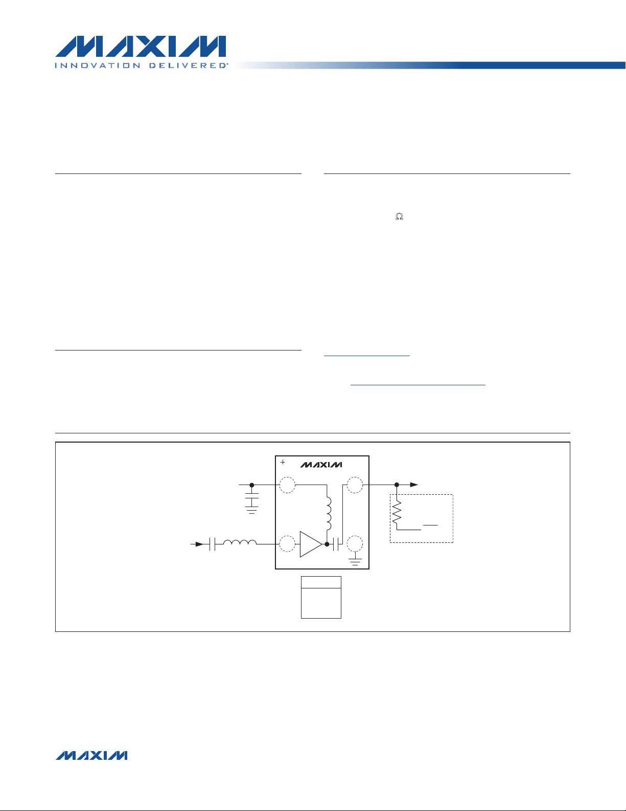
Typical Application Circuit
V
V
CC
C1
RF
INPUT
����������������������������������������������������������������� Maxim Integrated Products 1
CC
C2
L1
RFIN
MAX2691
A1 A2
B1 B2
MAX2691
L1 = 8.2nH
C1 = 100nF
C2 = 10pF
RFOUT
OPTIONAL SHUTDOWN
GND
R1
25kI
RF
OUTPUT
SHDN
For pricing, delivery, and ordering information, please contact Maxim Direct at 1-888-629-4642,
or visit Maxim’s website at www.maxim-ic.com.
Page 2
MAX2691
L2 Band GPS Low-Noise Amplifier
ABSOLUTE MAXIMUM RATINGS
VCC to GND .......................................................... -0.3V to +3.6V
Other Pins to GND
(except RFIN) ...................-0.3V to (+ Operating VCC + 0.3V)
Maximum Current into RF Input .........................................10mA
Maximum RF Input Power ............................................... +5dBm
Continuous Power Dissipation (TA = +70°C)
4-Bump WLP (derates 9.7mW/°C above +70°C) ........776mW
Note 1: Refer to Application Note 1891: Wafer-Level Packaging (WLP) and Its Applications.
CAUTION! ESD SENSITIVE DEVICE
Stresses beyond those listed under “Absolute Maximum Ratings” may cause permanent damage to the device. These are stress ratings only, and functional operation of the device at these or any other conditions beyond those indicated in the operational sections of the specifications is not implied. Exposure to absolute
maximum rating conditions for extended periods may affect device reliability.
DC ELECTRICAL CHARACTERISTICS
(MAX2691 EV kit, VCC = 1.6V to 3.6V, TA = -40°C to +85°C, no RF signals are applied. Typical values are at VCC = 2.85V and
TA = +25°C, unless otherwise noted.) (Note 2)
Operating Temperature Range .......................... -40°C to +85°C
Junction Temperature .....................................................+150°C
Storage Temperature Range ............................ -65°C to +160°C
Lead Temperature (soldering, 10s) ........Reflow Profile (Note 1)
Soldering Temperature (reflow) ......................................+260°C
PARAMETER CONDITIONS MIN TYP MAX UNITS
Supply Voltage 1.6 2.85 3.6 V
Supply Current
Digital Input Logic-High (Note 3) 1.2 V
Digital Input Logic-Low (Note 3) 0.45 V
SHDN = high
Shutdown mode, SHDN = low
4.3 mA
4.0 20 µA
AC ELECTRICAL CHARACTERISTICS
(MAX2691 EV kit, VCC = 1.6V to 3.6V, TA = -40°C to +85°C, f
unless otherwise noted.) (Note 2)
PARAMETER CONDITIONS MIN TYP MAX UNITS
RF Frequency L2 band 1227 MHz
Power Gain (Note 4)
Noise Figure VCC = 1.6V to 3.3V 0.93 dB
In-Band 3rd-Order Input
Intercept Point
Input 1dB Compression Point (Note 6) -8.5 dBm
Input Return Loss 10.9 dB
VCC = 2.85V 13.3 17.5
VCC = 1.6V 13.1 17.4
(Note 5) -3.0 dBm
= 1227MHz. Typical values are at VCC = 2.85V and TA = +25°C,
RFIN
dB
����������������������������������������������������������������� Maxim Integrated Products 2
Page 3
MAX2691
L2 Band GPS Low-Noise Amplifier
AC ELECTRICAL CHARACTERISTICS (continued)
(MAX2691 EV kit, VCC = 1.6V to 3.6V, TA = -40°C to +85°C, f
unless otherwise noted.) (Note 2)
PARAMETER CONDITIONS MIN TYP MAX UNITS
Output Return Loss 15.6 dB
Reverse Isolation 45 dB
Note 2: Min and max limits guaranteed by test at TA = +25°C and guaranteed by design and characterization at TA = -40°C and
TA = +85°C, unless otherwise noted.
Note 3: Min and max limits guaranteed by test at TA = +25°C.
Note 4: Min limit guaranteed by design and characterization.
Note 5: Measured with the two tones located at 1MHz and 2MHz offset from the center of the GPS band with -30dBm/tone.
Note 6: Measured with a tone located at 5MHz offset from the center of the GPS band.
= 1227MHz. Typical values are at VCC = 2.85V and TA = +25°C,
RFIN
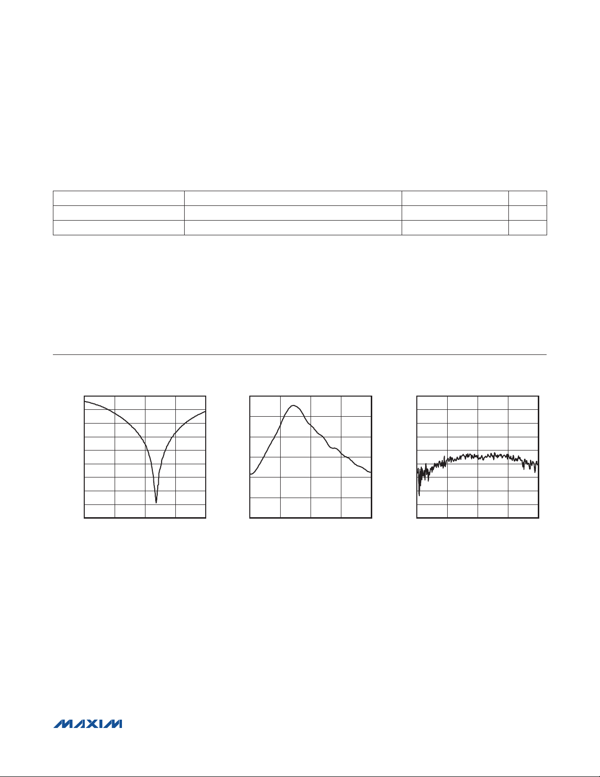
Typical Operating Characteristics
(MAX2691 EV kit. Typical values are at VCC = 2.85V, TA = +25°C, and f
INPUT RETURN LOSS vs. FREQUENCY
0
-5
-10
-15
-20
(dB)
|
S11
-25
|
-30
-35
-40
-45
500 2500
FREQUENCY (MHz)
200015001000
MAX2691 toc01
20
15
10
5
GAIN (dB)
0
-5
-10
500 2500
GAIN vs. FREQUENCY
FREQUENCY (MHz)
= 1227MHz, unless otherwise noted.)
RFIN
REVERSE ISOLATION vs. FREQUENCY
0
-10
MAX2691 toc02
-20
-30
-40
(dB)
|
S12
-50
|
-60
-70
-80
200015001000
-90
500 2500
MAX2691 toc03
200015001000
FREQUENCY (MHz)
����������������������������������������������������������������� Maxim Integrated Products 3
Page 4
MAX2691
L2 Band GPS Low-Noise Amplifier
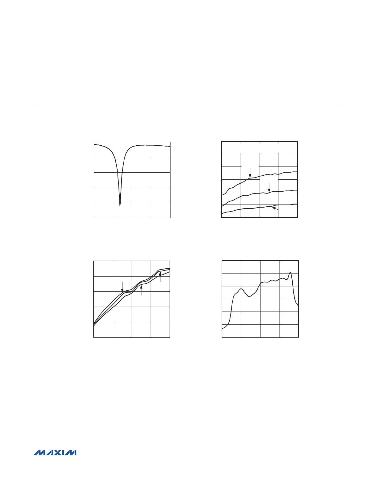
Typical Operating Characteristics (continued)
(MAX2691 EV kit. Typical values are at VCC = 2.85V, TA = +25°C, and f
OUTPUT RETURN LOSS vs. FREQUENCY
0
-5
-10
(dB)
|
S22
|
-15
-20
-25
500 2500
FREQUENCY (MHz)
200015001000
MAX2691 toc04
INPUT P1dB COMPRESSION vs.
SUPPLY VOLTAGE AND TEMPERATURE
-6
-8
-10
-12
INPUT P1dB (dBm)
-14
TA = -40°C
T
= +85°C
A
T
A
MAX2691 toc06
= +25°C
= 1227MHz, unless otherwise noted.)
RFIN
INBAND IIP3 vs. SUPPLY VOLTAGE
AND TEMPERATURE
2
TWO TONES LOCATED AT +1MHz AND +2MHz
FROM 1227MHz. P
1
0
-1
IIP3 (dBm)
-2
-3
-4
1.6 3.6
= -30dBm/TONE
IN
TA = -40°C
TA = +25°C
SUPPLY VOLTAGE (V)
1dB GAIN DESENSE vs.
BLOCKER FREQUENCY
5
0
-5
(dBm)
-10
-15
BLOCKER POWER
-20
MAX2691 toc05
TA = +85°C
3.12.62.1
MAX2691 toc07
-16
1.6 3.6
SUPPLY VOLTAGE (V)
3.12.62.1
-25
500 2500
BLOCKER FREQUENCY (MHz)
200015001000
����������������������������������������������������������������� Maxim Integrated Products 4
Page 5

L2 Band GPS Low-Noise Amplifier
Bump Configuration
TOP VIEW
+
V
A1 A2
CC
MAX2691
B1 B2
RFIN
WLP
BUMP NAME FUNCTION
A1 V
A2
B1 RFIN RF Input. Requires a DC-blocking capacitor and external matching components.
B2 GND Ground. Connect to the PCB ground plane.
CC
RFOUT
(SHDN)
Supply Voltage. Bypass to ground with a 10pF capacitor as close as possible to the IC.
RF Output/SHDN Input. RFOUT is internally matched to 50I and pulled up to VCC through a 1MI
resistor. SHDN is shared with the RFOUT bump. The device is in active mode by default once VCC
is applied. RFOUT(SHDN) can be pulled to a DC low through a 25kI resistor to shut down the IC.
RFOUT (SHDN)
GND
Bump Description
MAX2691
Detailed Description
The MAX2691 LNA is designed for GPS L2 applications.
The device features a power-shutdown control mode
to eliminate the need for an external supply switch.
The device achieves high gain, low noise figure, and
excellent linearity.
Input and Output Matching
The MAX2691 requires an off-chip input match. Only an
inductor in series with a DC-blocking capacitor is needed
to form the input matching circuit. The Typical Application
Circuit shows the recommended input-matching network.
These values are optimized for the best simultaneous gain, noise figure, and return loss performance.
Reducing the input coupling capacitor results in a lower
IIP3. The device integrates an on-chip output matching
to 50I at the output, eliminating the need for external
matching components. Table 1 lists typical device S
parameters and Kf values. Typical noise parameters are
shown in Table 2.
Shutdown
The MAX2691 includes an optional shutdown feature to
turn off the entire chip. The device is placed in active
mode by default once VCC is applied, due to the on-chip
pullup resistor to VCC at the RFOUT bump (shared with
the SHDN input). To shut down the part, apply a logic-low
to the RFOUT bump through an external resistor with an
adequate value, e.g., 25kI, in order not to load the RF
output signal during active operation.
Applications Information
A properly designed PCB is essential to any RF microwave circuit. Use controlled-impedance lines on all
high-frequency inputs and outputs. Bypass VCC with
decoupling capacitors located close to the device. For
long VCC lines, it may be necessary to add decoupling
capacitors. Locate these additional capacitors further
away from the device package. Proper grounding of
the GND pin is essential. If the PCB uses a topside RF
ground, connect it directly to the GND pin. For a board
where the ground is not on the component layer, connect
the GND pin to the board with multiple vias close to the
package.
Refer to www.maxim-ic.com for the MAX2691 EV kit
schematic, Gerber data, PADS layout file, and BOM
information.
����������������������������������������������������������������� Maxim Integrated Products 5
Page 6

L2 Band GPS Low-Noise Amplifier
Table 1. Typical S Parameter Values and K-Factor
MAX2691
FREQ.
(MHz)
700 -2.1 -78.1 3.5 -175.7 -54.0 113.3 -1.3 -124.9 16.75126
800 -2.5 -87.1 6.0 175.7 -47.7 112.0 -1.6 -143.3 8.847551
900 -2.8 -96.2 8.8 163.0 -55.5 85.4 -2.4 -162.8 22.33037
1000 -3.1 -104.3 11.7 146.2 -53.8 54.0 -3.9 175.0 19.54059
1100 -3.4 -112.3 14.4 119.2 -46.3 33.8 -8.3 149.5 9.366309
1200 -3.7 -119.4 16.0 83.5 -46.9 15.3 -19.1 -126.9 9.788318
1220 -3.7 -120.7 16.1 75.6 -47.6 -1.0 -14.2 -114.7 10.25069
1240 -3.7 -122.4 16.0 67.9 -49.4 20.3 -10.9 -114.4 12.09861
1260 -3.8 -123.7 15.9 60.1 -49.7 14.9 -8.7 -118.5 12.1323
1280 -3.8 -125.0 15.6 52.8 -47.3 -6.0 -6.9 -124.3 8.793041
1300 -3.8 -126.6 15.2 46.0 -43.5 19.6 -5.7 -130.2 5.277003
1400 -4.0 -133.5 13.4 18.4 -44.9 -22.8 -2.6 -157.6 4.94144
1500 -4.1 -140.3 11.3 -0.5 -48.5 -21.4 -1.6 -179.3 6.656188
1600 -4.1 -147.6 9.4 -15.6 -47.7 -23.6 -1.3 163.8 5.983826
1700 -4.1 -154.6 7.8 -28.5 -44.8 -16.5 -1.0 148.8 4.18904
S11 MAG
(dB)
S11
PHASE
(DEGREES)
S21 MAG
(dB)
S21
PHASE
(DEGREES)
S12 MAG
(dB)
S12
PHASE
(DEGREES)
S22 MAG
(dB)
S22
PHASE
(DEGREES)
Table 2. Typical Noise Parameters (VCC = 2.85V, TA = +25NC)
FREQUENCY (MHz) FMIN (dB)
1200 0.66 0.45 47 8.37
1210 0.66 0.45 48 8.35
1220 0.66 0.45 48 8.33
1230 0.66 0.45 48 8.30
1240 0.66 0.45 49 8.28
1250 0.66 0.45 49 8.26
1260 0.66 0.45 50 8.24
1270 0.67 0.45 50 8.22
1280 0.67 0.44 50 8.20
1290 0.67 0.44 51 8.18
1300 0.67 0.44 51 8.17
|G
| |G
OPT
OPT
| ANGLE
RN (I)
K
f
Ordering Information
PART TEMP RANGE PIN-PACKAGE
MAX2691EWS+T
+Denotes a lead(Pb)-free/RoHS-compliant package.
T = Tape and reel.
-40NC to +85NC
4 WLP
Chip Information
PROCESS: SiGe BiCMOS
����������������������������������������������������������������� Maxim Integrated Products 6
Package Information
For the latest package outline information and land patterns
(footprints), go to www.maxim-ic.com/packages. Note that a
“+”, “#”, or “-” in the package code indicates RoHS status only.
Package drawings may show a different suffix character, but
the drawing pertains to the package regardless of RoHS status.
PACKAGE
TYPE
4 WLP W40A0+1
PACKAGE
CODE
OUTLINE
NO.
21-0480
LAND
PATTERN NO.
Refer to Application
Note 1891
Page 7

MAX2691
L2 Band GPS Low-Noise Amplifier
Revision History
REVISION
NUMBER
0 12/11 Initial release —
REVISION
DATE
DESCRIPTION
PAGES
CHANGED
Maxim cannot assume responsibility for use of any circuitry other than circuitry entirely embodied in a Maxim product. No circuit patent licenses are implied.
Maxim reserves the right to change the circuitry and specifications without notice at any time. The parametric values (min and max limits) shown in the Electrical
Characteristics table are guaranteed. Other parametric values quoted in this data sheet are provided for guidance.
Maxim Integrated Products, 120 San Gabriel Drive, Sunnyvale, CA 94086 408-737-7600 7
©
2011 Maxim Integrated Products Maxim is a registered trademark of Maxim Integrated Products, Inc.
 Loading...