Maxim MAX2690EUB Datasheet

MAX2690
Low-Noise, 2.5GHz
Downconverter Mixer
________________________________________________________________
Maxim Integrated Products
1
19-1282; Rev 0; 10/97
EVALUATION KIT
AVAILABLE
For free samples & the latest literature: http://www.maxim-ic.com, or phone 1-800-998-8800.
For small orders, phone 408-737-7600 ext. 3468.
_______________General Description
The MAX2690 is a miniature, low-noise, low-power
downconverter mixer designed for use in portable consumer equipment. Signals at the RF input port are
mixed with signals at the local-oscillator (LO) port using
a double-balanced mixer. The RF port frequency range
is 400MHz to 2500MHz. The LO port frequency range is
700MHz to 2500MHz. The IF frequency range is 10MHz
to 500MHz, provided the LO and RF frequencies are
chosen appropriately.
The IF port is differential, which provides good linearity
and low LO emissions, as well as providing compatibility with applications using differential IF filters, such as
CDMA cellular phones. The mixer noise figure is 10dB
at 900MHz.
The MAX2690 draws 16mA at VCC= 3V and operates
from a +2.7V to +5.5V supply. A logic-controlled shutdown mode reduces the supply current to less than 1µA,
making it ideal for battery-operated equipment. This
device is offered in a miniature 10-pin µMAX package.
________________________Applications
2.45GHz Industrial-Scientific-Medical (ISM)
Band Radios
Wireless Local Area Networks (WLANs)
Personal Communications Systems (PCS)
Code-Division Multiple Access (CDMA)
Communications Systems
Cellular and Cordless Phones
Hand-Held Radios
____________________________Features
♦ 7.6dBm Input Third-Order Intercept Point
♦ 10dB Downconverter Mixer Noise Figure
♦ 7.9dB Gain
♦ 400MHz to 2500MHz Wideband Operation
♦ Low Cost
♦ +2.7V to +5.5V Single-Supply Operation
♦ <1µA Shutdown Mode
♦ Ultra-Small 10-Pin µMAX Package
PART
MAX2690EUB -40°C to +85°C
TEMP. RANGE PIN-PACKAGE
10 µMAX
______________Ordering Information
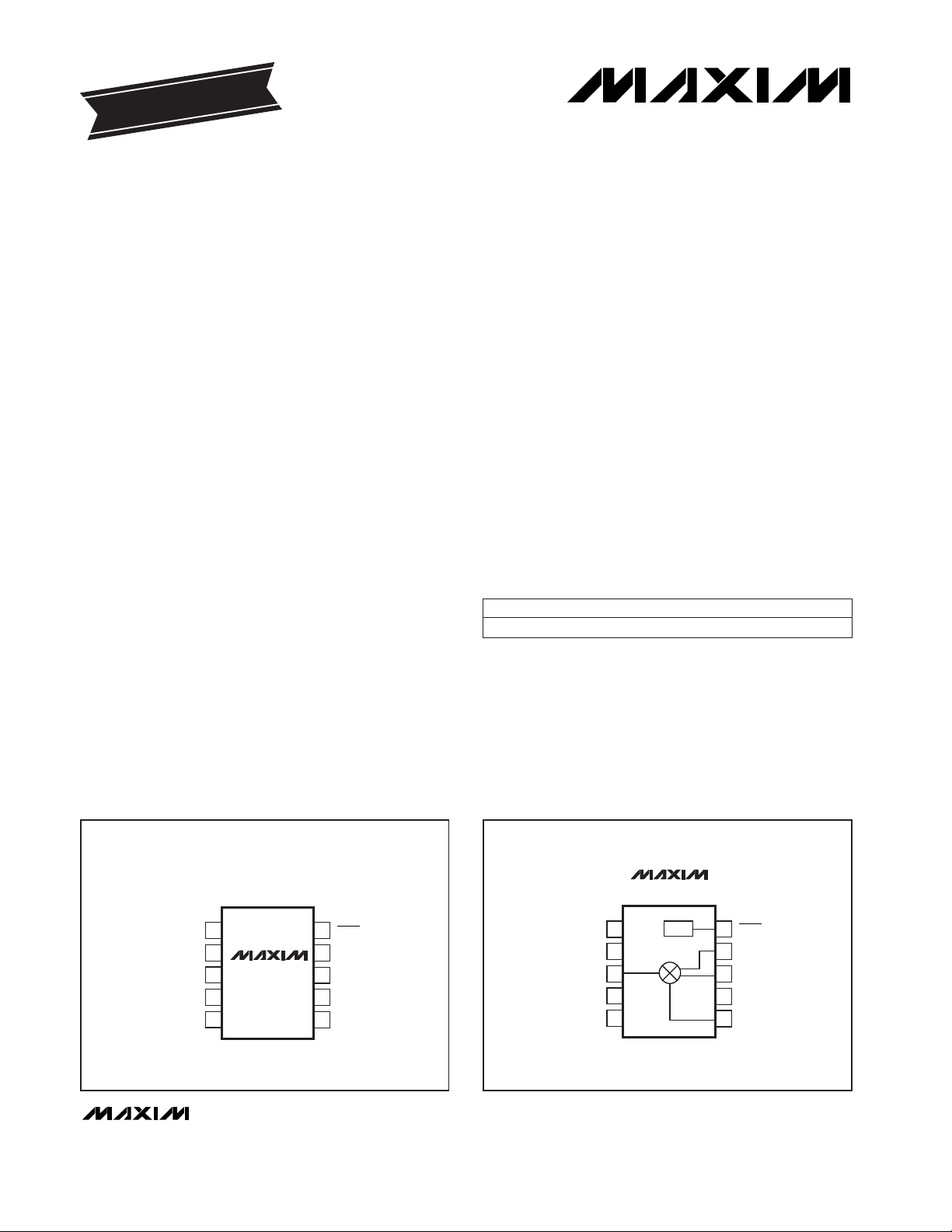
__________________Pin Configuration
1
2
3
4
5
10
9
8
7
6
SHDN
IFOUT+
IFOUTGNDLORFBYP
RFIN
GND
LGND
MAX2690
µMAX
TOP VIEW
LOV
CC
________________Functional Diagram
1
2
3
4
5
10
9
8
7
6
SHDN
IFOUT+
IFOUTGNDLORFBYP
RFIN
GND
LGND
MAX2690
µMAX
TOP VIEW
LOV
CC
BIAS
Typical Operating Circuit appears at end of data sheet.

MAX2690
Low-Noise, 2.5GHz
Downconverter Mixer
2 _______________________________________________________________________________________
ABSOLUTE MAXIMUM RATINGS
DC ELECTRICAL CHARACTERISTICS
(VCC= +2.7V to +5.5V, no RF signals applied, LO = open, IFOUT+ = IFOUT- = VCC, SHDN = high, LGND = GND = GNDLO = 0V,
T
A
= T
MIN
to T
MAX
. Typical values are at VCC= +3.0V and TA= +25°C, unless otherwise noted. Minimum and maximum values are
guaranteed by design and characterization over temperature.)
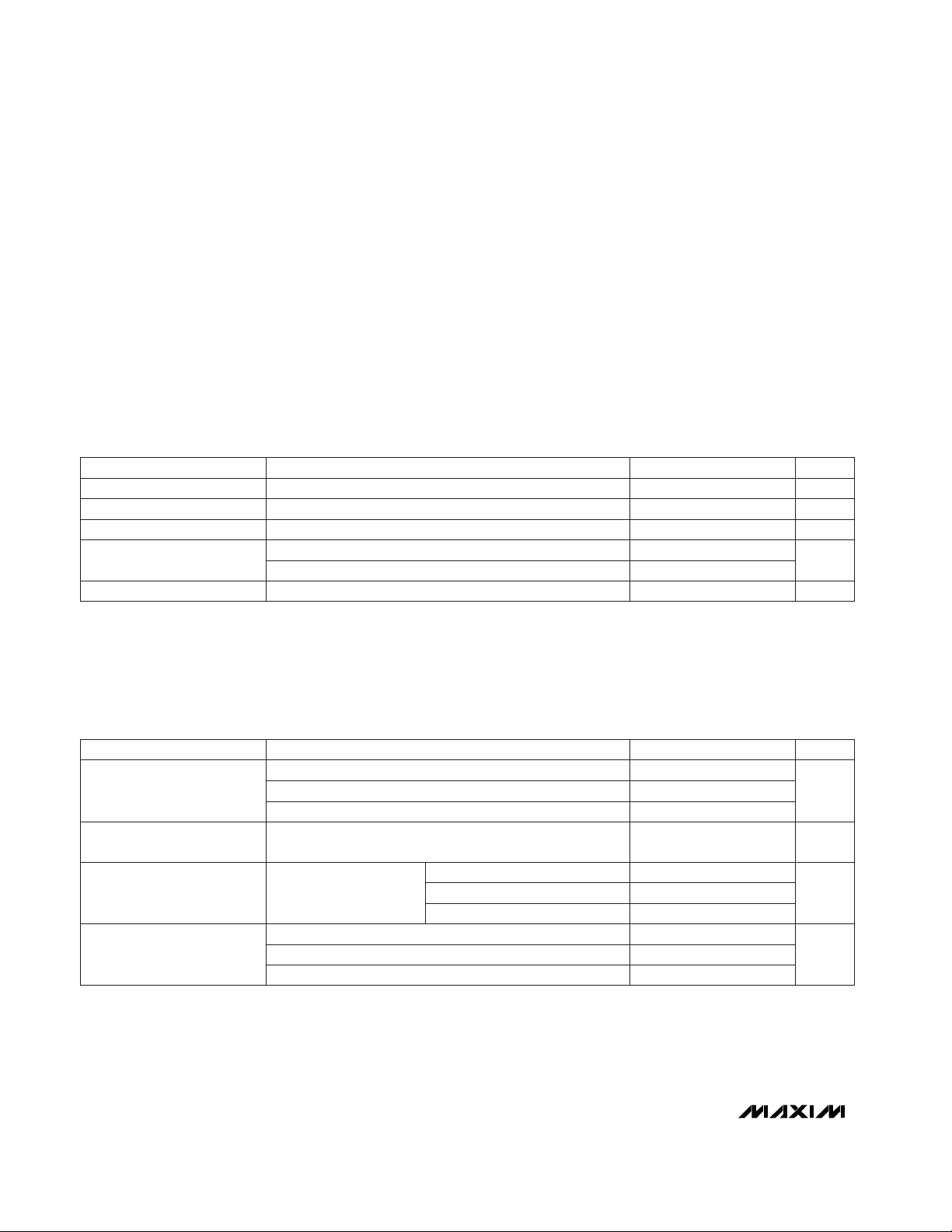
AC ELECTRICAL CHARACTERISTICS
(MAX2690 EV kit; VCC= +3.0V; PLO= -3dBm; PRF= -25dBm; SHDN = high; RFIN matched for 900MHz, 1.95GHz, and 2.45GHz as
noted below. Inductor connected from LGND to GND = 39nH for 900MHz operation, 27nH for 1.95GHz operation, and 6.8nH for
2.45GHz operation. T
A
= +25°C, unless otherwise noted.)
Stresses beyond those listed under “Absolute Maximum Ratings” may cause permanent damage to the device. These are stress ratings only, and functional
operation of the device at these or any other conditions beyond those indicated in the operational sections of the specifications is not implied. Exposure to
absolute maximum rating conditions for extended periods may affect device reliability.
VCCto GND...........................................................-0.3V to +6.0V
RFIN Input Power..............................................................10dBm
LO Input Power.................................................................10dBm
SHDN Input Voltage...................................-0.3V to (V
CC
+ 0.3V)
Continuous Power Dissipation
10-Pin µMAX (derate 4.1mW/°C above +70°C)............330mW
Operating Temperature Range
MAX2690EUB...................................................-40°C to +85°C
Junction Temperature......................................................+150°C
Storage Temperature Range.............................-65°C to +165°C
Lead Temperature (soldering, 10sec).............................+300°C
SHDN = 0V
SHDN = low
0V < SHDN < V
CC
CONDITIONS
V0.5Shutdown Input Voltage Low
V2
mA9.5 16 20.1Operating Supply Current
Shutdown Input Voltage High
0.4
µA
2
Shutdown Supply Current
µA-5 4 25Shutdown Input Bias Current
UNITSMIN TYP MAXPARAMETER
fRF= 2.45GHz, fLO= 2.1GHz
fRF= 1.95GHz, fLO= 1.75GHz
fRF= 900MHz, fLO= 1.1GHz
fRF= 1.95GHz, TA= T
MIN
to T
MAX
(Note 2)
CONDITIONS
dB
4
6.4
7.9
Conversion Gain
(Note 1)
dB±0.6 ±1.2
Gain Variation over
Temperature
UNITSMIN TYP MAXPARAMETER
Two tones at
-25dBm per tone,
f
RF2
= 1MHz above f
RF
fRF= 900MHz, fLO= 1.1GHz
dBm
4.3
5.3
7.6
Input Third-Order Intercept
10
fRF= 2.45GHz, fLO= 2.1GHz
fRF= 1.95GHz, fLO= 1.75GHz
dB
12
Noise-Figure
Single Sideband
11.5
fRF= 900MHz, fLO= 1.1GHz
fRF= 1.95GHz, fLO= 1.75GHz
fRF= 2.45GHz, fLO= 2.1GHz

MAX2690
Low-Noise, 2.5GHz
Downconverter Mixer
_______________________________________________________________________________________ 3
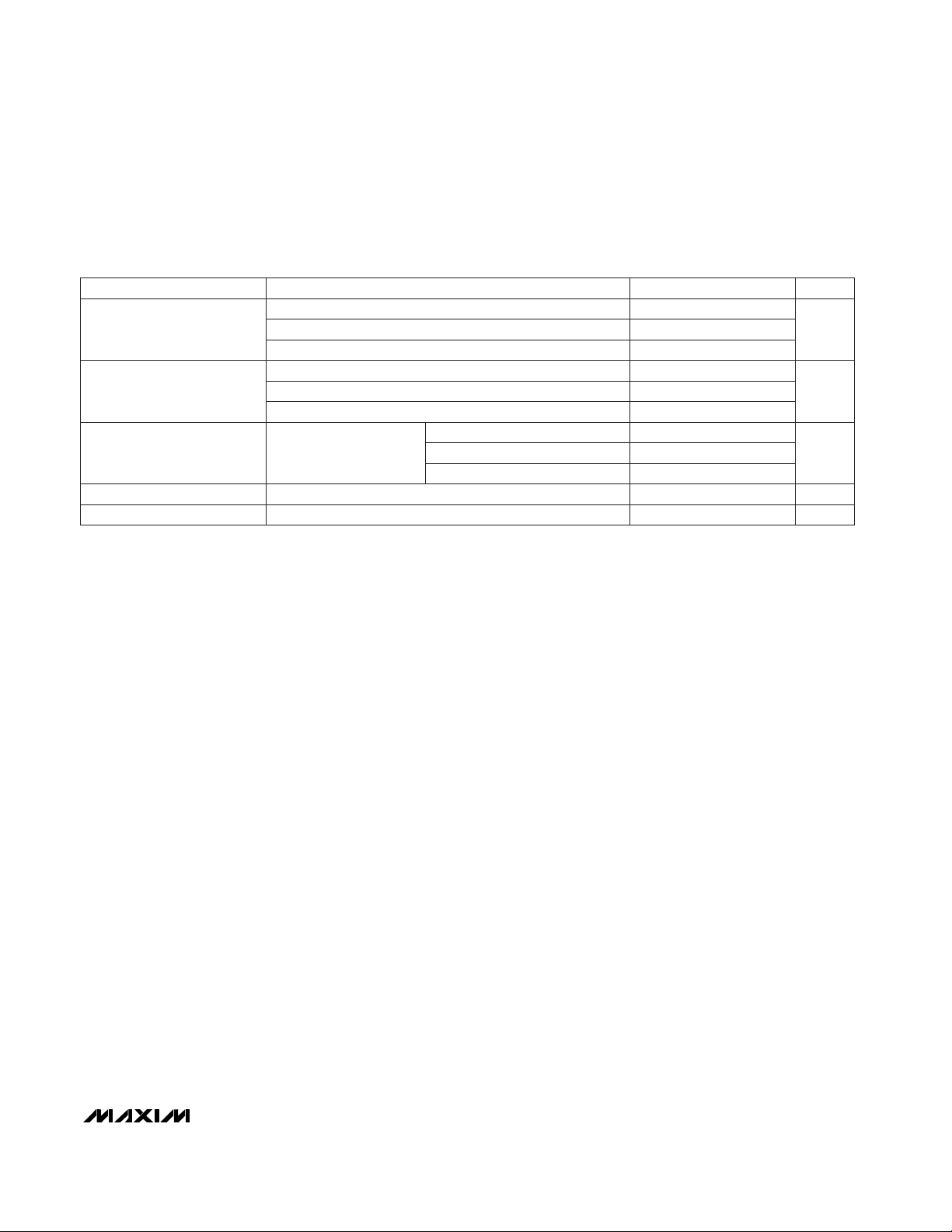
AC ELECTRICAL CHARACTERISTICS (continued)
(MAX2690 EV kit; VCC= +3.0V; PLO= -3dBm; PRF= -25dBm; SHDN = high; RFIN matched for 900MHz, 1.95GHz, and 2.45GHz as
noted below. Inductor connected from LGND to GND = 39nH for 900MHz operation, 27nH for 1.95GHz operation, and 6.8nH for
2.45GHz operation. T
A
= +25°C, unless otherwise noted.)
Note 1: Consult the
Applications Information
section for information on designing a matching network.
Note 2: Guaranteed by design and characterization.
Note 3: This spurious response is caused by a higher-order mixing product (2x2). Specified RF frequency is applied and IF output
power is observed at the desired IF frequency (200MHz for f
RF
= 900MHz, or 1.95GHz, and 350MHz for fRF= 2.45GHz).
Note 4: From the time SHDN goes high to the time I
CC
reaches 90% of its final value (on), or from the time SHDN goes low to the
time I
CC
drops below 10µA (off).
fRF= 2.45GHz, fLO= 2.1GHz
fRF= 1.95GHz, fLO= 1.75GHz
fRF= 900MHz, fLO= 1.1GHz
-74
RF input = -15dBm
(Note 4)
dBm
CONDITIONS
-56
IF/2 Spurious Response
(Note 3)
-62
µs1Turn-On Time
dBm
-28
-32
-32
LO Emission at IF Port
UNITSMIN TYP MAXPARAMETER
fRF= 2.45GHz, fLO= 2.1GHz
fRF= 1.95GHz, fLO= 1.75GHz
fRF= 900MHz, fLO= 1.1GHz
dBm
-25
-27
-30
LO Emission at RF Port
(Note 4) µs1.6Turn-Off Time
fRF= 1.0GHz, fLO= 1.1GHz
fRF= 1.85GHz, fLO= 1.75GHz
fRF= 2.275GHz, fLO= 2.1GHz
 Loading...