MAXIM MAX2686, MAX2688 Technical data

19-5456; Rev 0; 8/10
EVALUATION KIT
AVAILABLE
GPS/GNSS Low-Noise Amplifiers
General Description
The MAX2686/MAX2688 low-noise amplifiers (LNAs) are
designed for GPS L1, Galileo, and GLONASS applications. Designed in Maxim’s advanced SiGe process,
the devices achieve high gain and ultra-low-noise figure
while maximizing the input-referred 1dB compression
point and the 3rd-order intercept point. The MAX2686
provides a high gain of 19dB. The MAX2688 supplies
15dB of gain while attaining higher linearity.
The devices operate from a +1.6V to +3.3V single supply. The optional shutdown feature in the devices reduces the supply current to less than 10FA. The devices
are available in a very small, lead-free, RoHS-compliant,
0.86mm x 0.86mm x 0.65mm wafer-level package (WLP).
Applications
Automotive Navigation
Telematics (Asset Tracking and Management)
Personal Navigation Devices (PNDs)
Cellular Phones with GPS
Notebook PCs/Ultra-Mobile PCs
Recreational, Marine Navigation
Avionics
Watches
Digital Cameras
Features
S High-Power Gain: 19dB (MAX2686)
S Ultra-Low-Noise Figure: 0.75dB (MAX2686)
S Integrated 50Ω Output Matching Circuit
S Low Supply Current: 4.1mA
S Wide Supply Voltage Range: 1.6V to 3.3V
S Low Bill of Materials: One Inductor, Two
Capacitors
S Small Footprint: 0.86mm x 0.86mm
S Thin Profile: 0.65mm
S 0.4mm-Pitch Wafer-Level Package (WLP)
Ordering Information
PART TEMP RANGE PIN-PACKAGE
MAX2686EWS+T
MAX2688EWS+T
+Denotes a lead(Pb)-free/RoHS-compliant package.
T = Tape and reel.
-40NC to +85NC
-40NC to +85NC
4 WLP
4 WLP
MAX2686/MAX2688
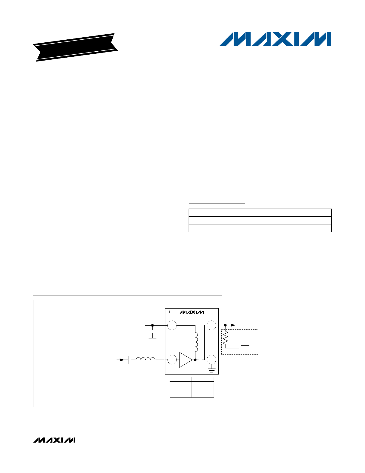
Typical Application Circuit
MAX2686
V
V
CC
C1
RF
INPUT
_______________________________________________________________ Maxim Integrated Products 1
CC
C2
L1
RFIN
MAX2688
A1 A2
B1 B2
MAX2686
L1 = 6.8nH
C1 = 100nF
C2 = 10pF
MAX2688
L1 = 6.2nH
C1 = 100nF
C2 = 10pF
For pricing, delivery, and ordering information, please contact Maxim Direct at 1-888-629-4642,
or visit Maxim’s website at www.maxim-ic.com.
RFOUT
RF
OUTPUT
R1
25kI
OPTIONAL SHUTDOWN
GND
SHDN

GPS/GNSS Low-Noise Amplifiers
ABSOLUTE MAXIMUM RATINGS
VCC to GND ..........................................................-0.3V to +3.6V
Other Pins to GND ...............-0.3V to (+ Operating VCC + 0.3V)
Maximum RF Input Power ............................................... +5dBm
Continuous Power Dissipation (TA = +70°C)
4-Bump WLP (derates 9.7mW/°C above +70°C) ........776mW
Maximum Current into RF Input .........................................10mA
Note 1: Refer to Application Note 1891: Wafer-Level Packaging (WLP) and Its Applications.
CAUTION! ESD SENSITIVE DEVICE
Stresses beyond those listed under “Absolute Maximum Ratings” may cause permanent damage to the device. These are stress ratings only, and functional
operation of the device at these or any other conditions beyond those indicated in the operational sections of the specifications is not implied. Exposure to absolute
maximum rating conditions for extended periods may affect device reliability.
DC ELECTRICAL CHARACTERISTICS
(MAX2686/MAX2688 EV kit, VCC = 1.6V to 3.3V, TA = -40NC to +85NC, no RF signals are applied. Typical values are at VCC = 2.85V
MAX2686/MAX2688
and TA = +25NC, unless otherwise noted.) (Note 2)
PARAMETER CONDITIONS MIN TYP MAX UNITS
Supply Voltage 1.6 2.85 3.3 V
Supply Current
Digital Input Logic-High (Note 3) 1.2 V
Digital Input Logic-Low (Note 3) 0.45 V
SHDN = high
Shutdown mode, SHDN = low
Operating Temperature Range .......................... -40°C to +85°C
Junction Temperature .....................................................+150°C
Storage Temperature Range ............................ -65°C to +160°C
Lead Temperature (soldering, 10s) ........ Reflow Profile (Note 1)
Soldering Temperature (reflow) ......................................+260°C
MAX2686 4.1
MAX2688 4.1
10 µA
mA
AC ELECTRICAL CHARACTERISTICS
(MAX2686/MAX2688 EV kit, VCC = 1.6V to 3.3V, TA = -40NC to +85NC, f
TA = +25NC, unless otherwise noted.) (Note 2)
PARAMETER CONDITIONS MIN TYP MAX UNITS
RF Frequency L1 band 1575.42 MHz
VCC = 2.85V (Note 4)
Power Gain
VCC = 1.6V
Noise Figure VCC = 1.6V to 3.3V
In-Band 3rd-Order Input
Intercept Point
Out-of-Band 3rd-Order Input
Intercept Point
Input 1dB Compression Point (Note 7)
Input Return Loss 8.5 dB
2
(Note 5)
(Note 6)
MAX2686 14.7 19
MAX2688 11.9 15.4
MAX2686 14.4 18.9
MAX2688 11.6 15.3
MAX2686 0.75
MAX2688 0.8
MAX2686 -3
MAX2688 +4
MAX2686 0
MAX2688 +7
MAX2686 -10
MAX2688 -6
= 1575.42MHz. Typical values are at VCC = 2.85V and
RFIN
dBm
dBm
dBm
dB
dB

GPS/GNSS Low-Noise Amplifiers
AC ELECTRICAL CHARACTERISTICS (continued)
(MAX2686/MAX2688 EV kit, VCC = 1.6V to 3.3V, TA = -40NC to +85NC, f
TA = +25NC, unless otherwise noted.) (Note 2)
PARAMETER CONDITIONS MIN TYP MAX UNITS
Output Return Loss 15 dB
Reverse Isolation 40 dB
Note 2: Min and max limits guaranteed by test at TA = +25°C and guaranteed by design and characterization at TA = -40°C and
TA = +85°C, unless otherwise noted.
Note 3: Min and max limits guaranteed by test at TA = +25°C.
Note 4: Min limit guaranteed by design and characterization.
Note 5: Measured with the two tones located at 1MHz and 2MHz offset from the center of the GPS band with -27dBm/tone for the
MAX2686 and -24dBm/tone for the MAX2688.
Note 6: Measured with input tones at 1713MHz (-27dBm) and 1851MHz (-39dBm).
Note 7: Measured with a tone located at 5MHz offset from the center of the GPS band.
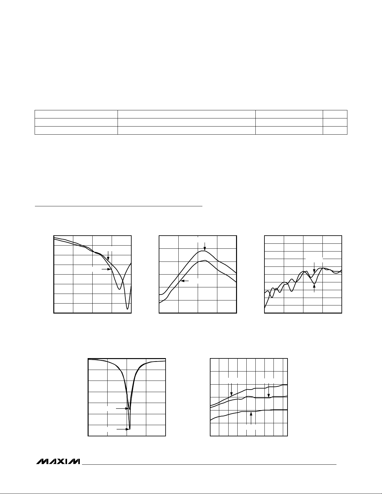
Typical Operating Characteristics
(MAX2686/MAX2688 EV kit. Typical values are at VCC = 2.85V, TA = +25°C, and f
= 1575.42MHz. Typical values are at VCC = 2.85V and
RFIN
= 1575.42MHz, unless otherwise noted.)
RFIN
MAX2686/MAX2688
INPUT RETURN LOSS vs. FREQUENCY
0
-5
-10
-15
-20
|S11| (dB)
-25
-30
-35
-40
500 2500
FREQUENCY (MHz)
MAX2688
MAX2686
200015001000
OUTPUT RETURN LOSS vs. FREQUENCY
0
-5
-10
-15
|S22| (dB)
-20
-25
-30
-35
MAX2686
MAX2688
500 2500
MAX2686 toc01
FREQUENCY (MHz)
25
20
15
10
GAIN (dB)
5
0
-5
500 2500
MAX2686
MAX2688
FREQUENCY (MHz)
vs. SUPPLY VOLTAGE AND TEMPERATURE
(TWO TONES LOCATED AT 1MHz AND 2MHz OFFSET WITH -30dBm/TONE)
0
GAIN vs. FREQUENCY
MAX2686 toc04
200015001000
-1
-2
-3
IIP3 (dBm)
-4
-5
-6
200015001000
MAX2686 IN-BAND IIP3
TA = -40°C
1.6
SUPPLY VOLTAGE (V)
MAX2686 toc02
TA = +85°C
REVERSE ISOLATION vs. FREQUENCY
-20
-25
-30
-35
-40
-45
|S12| (dB)
-50
-55
-60
-65
-70
500 2500
TA = +25°C
3.23.02.82.62.42.22.01.8
MAX2686
MAX2688
200015001000
FREQUENCY (MHz)
MAX2686 toc05
MAX2686 toc03
3
 Loading...