

19-5479; Rev 0; 8/10
EVALUATION KIT
AVAILABLE
Tiny Low-Noise Amplifiers for HSPA/LTE
General Description
The MAX2666/MAX2668 are a family of low-noise amplifiers (LNAs) intended for use in HSPA mobile handsets.
The LNAs provide three programmable gain states,
delivering superior optimization for linearity and sensitivity versus traditional two-gain-state LNAs.
The MAX2666 is optimized for use over the 2100MHz
to 2200MHz frequency range (bands 1, 4, and 10) and
offers a typical maximum gain of 14.5dB.
The MAX2668 is optimized for use over the 850MHz to
1000MHz frequency range (bands 5, 6, and 8) and provides a typical maximum gain of 17dB.
Each device is available in a tiny 1mm x 1.5mm, 6-pin
ultra-thin LGA package.
MAX2666/MAX2668
Features
S Small Footprint: 1mm x 1.5mm Package
S Thin Profile: 0.55mm
S Low Noise Figure
1dB for MAX2668
1.1dB for MAX2666
S Three Gain States for Optimum Blocker Handling
S 3.8mA Low Supply Current
S Low Bill of Materials
Ordering Information
Applications
HSPA/LTE Front-End Modules
HSPA/LTE Preamplification
PART TEMP RANGE PIN-PACKAGE
MAX2666EYT+
MAX2668EYT+
+Denotes a lead(Pb)-free/RoHS-compliant package.
-40NC to +85NC
-40NC to +85NC
6 Ultra-Thin LGA
6 Ultra-Thin LGA
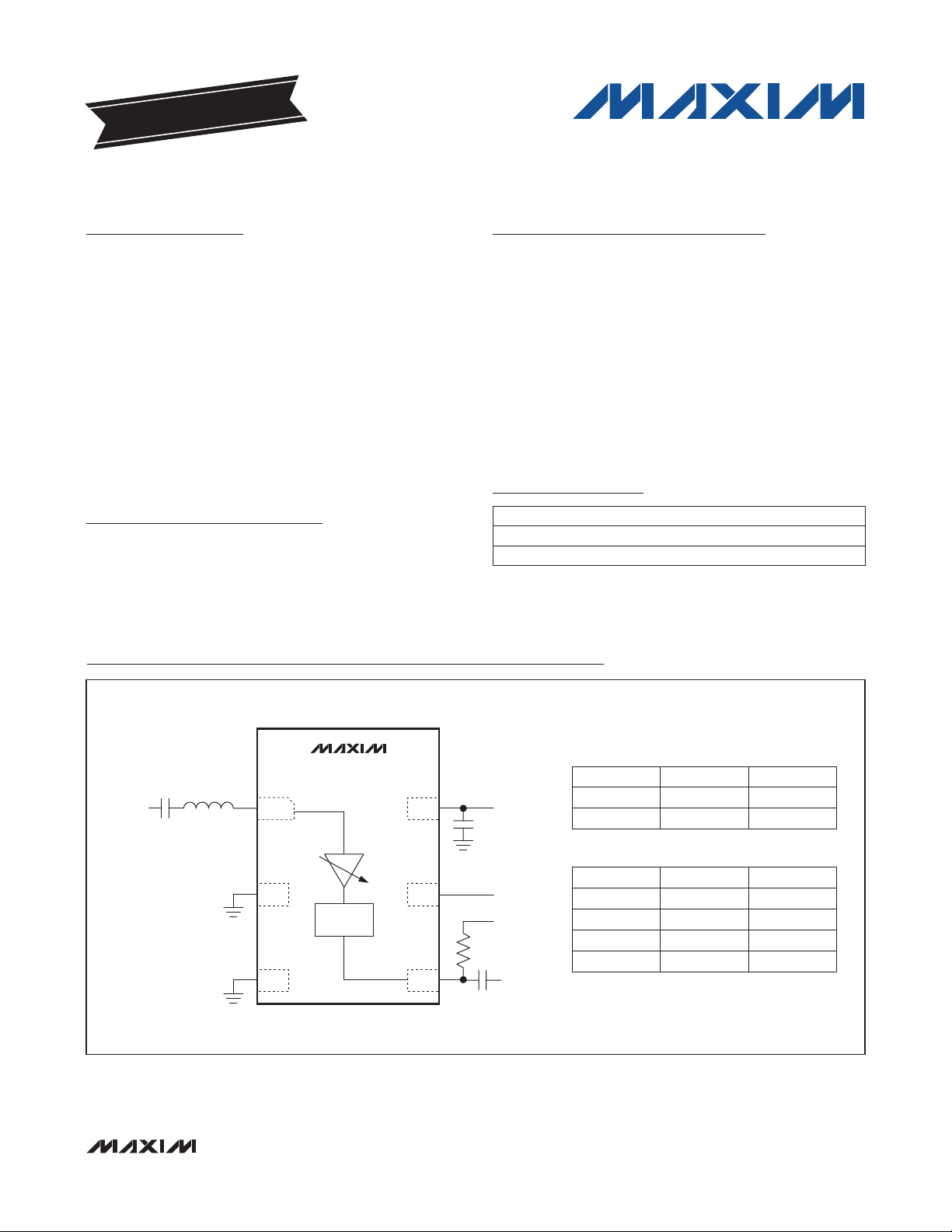
Typical Operating Circuit
GAIN CONTROL TABLE FOR TWO GAIN STEPS
GAIN1
0 — LOW
1 — HIGH
GAIN CONTROL TABLE FOR THREE GAIN STEPS
GAIN1
0 OFF
0 LOW
1 MID
1 HIGH
GAIN0 GAIN
GAIN0 GAIN
0
1
0
1
LNA_IN
MAX2666
MAX2668
1
2
CHOKE +
MATCHING
3
6
5
4
V
CC
GAIN1
GAIN0
LNA_OUT
_______________________________________________________________ Maxim Integrated Products 1
For pricing, delivery, and ordering information, please contact Maxim Direct at 1-888-629-4642,
or visit Maxim’s website at www.maxim-ic.com.
Tiny Low-Noise Amplifiers for HSPA/LTE
ABSOLUTE MAXIMUM RATINGS
VCC to GND ..........................................................-0.3V to +3.6V
Other Pins to GND ................................... -0.3V to (VCC + 0.3V)
Maximum Input Power ................................................... +10dBm
Continuous Power Dissipation (TA = +70NC)
Ultra-Thin LGA (derate 2.1mW/NC above +70NC) ....... 167mW
CAUTION! ESD SENSITIVE DEVICE
Stresses beyond those listed under “Absolute Maximum Ratings” may cause permanent damage to the device. These are stress ratings only, and functional
operation of the device at these or any other conditions beyond those indicated in the operational sections of the specifications is not implied. Exposure to absolute
maximum rating conditions for extended periods may affect device reliability.
DC ELECTRICAL CHARACTERISTICS
(Typical Operating Circuit, MAX2666/MAX2668 Evaluation Kit, GAIN1 = High, GAIN0 = High-Z, VCC = 2.7V to 3.3V, no RF signal
applied, TA = -40NC to +85NC. Typical values are at VCC = 2.85V, TA = +25NC, unless otherwise noted.) (Note 1)
MAX2666/MAX2668
Supply Voltage 2.7 2.85 3.3 V
Supply Current, High Gain GAIN_ = 11 3.8 mA
Supply Current, Mid Gain GAIN_ = 10 3.8 mA
Supply Current, Low Gain GAIN_ = 01 100 FA
Shutdown Current GAIN_ = 00 100 FA
Logic-High (VIH) 1.2 V
Logic-Low (VIL) 0.5 V
PARAMETER CONDITIONS MIN TYP MAX UNITS
Operating Temperature Range .......................... -40NC to +85NC
Junction Temperature .....................................................+150NC
Storage Temperature Range ............................ -65NC to +160NC
Lead Temperature (soldering, 10s) ................................+260NC
Soldering Temperature (reflow) ......................................+260NC
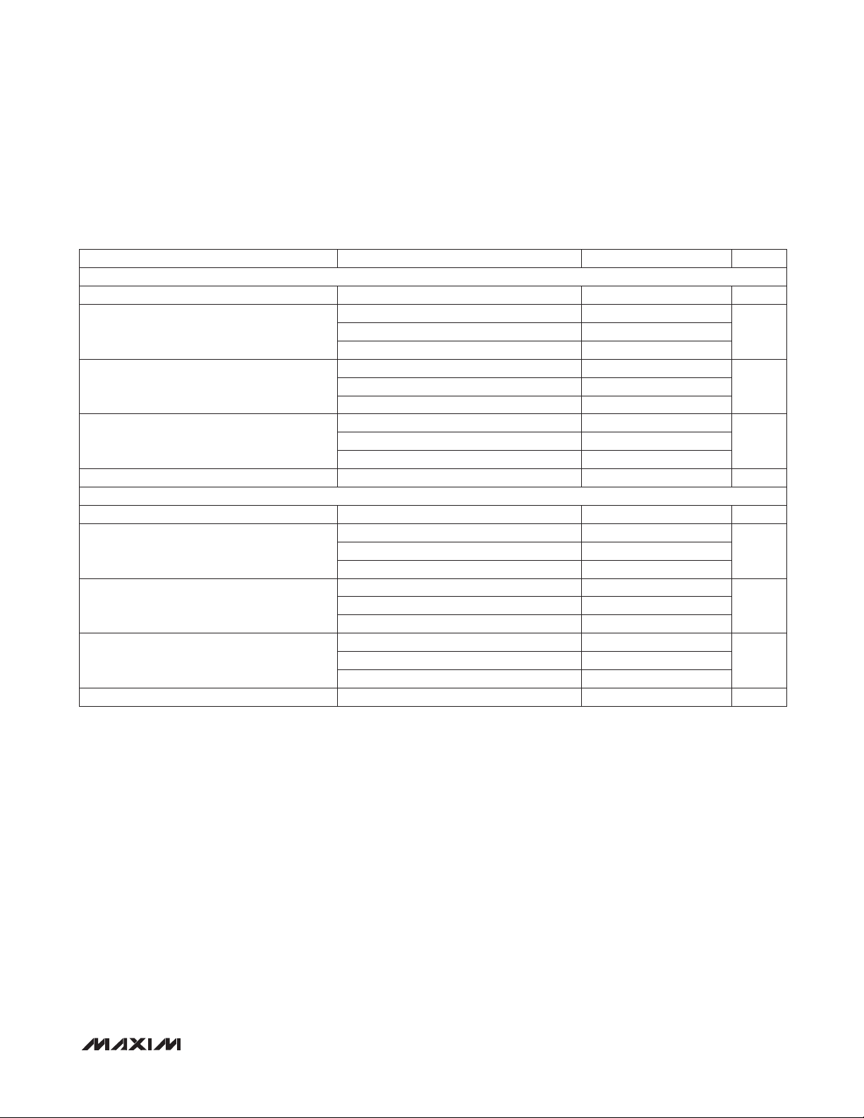
AC ELECTRICAL CHARACTERISTICS
(MAX2666/MAX2668 Evaluation Kit, input matching network according to Table 1 (input matching network), GAIN1 = High, GAIN0 =
High-Z, VCC = 2.85V, TA = +25NC, unless otherwise noted.)
PARAMETER CONDITIONS MIN TYP MAX UNITS
MAX2666
Frequency Range Bands 1, 4, 10 2110 2140 2170 MHz
HG mode 10 14.5 17.5
Gain
LG mode, GAIN_ = 01 -15.5 -12 -9
HG mode 1.1
Noise Figure
LG mode, GAIN_ = 01 12
HG mode -2
Input 3rd-Order Intercept (Note 2)
LG mode, GAIN_ = 01 > 20
Phase Shift with Gain Step 15 Degrees
2 ______________________________________________________________________________________
dBMG mode, GAIN_ = 10 0 5 8.5
dBMG mode, GAIN_ = 10 3
dBmMG mode, GAIN_ = 10 4
Tiny Low-Noise Amplifiers for HSPA/LTE
AC ELECTRICAL CHARACTERISTICS (continued)
(MAX2666/MAX2668 Evaluation Kit, input matching network according to Table 1 (input matching network), GAIN1 = High, GAIN0 =
High-Z, VCC = 2.85V, TA = +25NC, unless otherwise noted.)
PARAMETER CONDITIONS MIN TYP MAX UNITS
MAX2668 (BAND 8)
Frequency Range Band 8 925 942 960 MHz
HG mode 13.5 17 21
Gain
LG mode, GAIN_ = 01 -19 -16 -13
HG mode 1
Noise Figure
LG mode, GAIN_ = 01 16
HG mode -4
Input 3rd-Order Intercept (Note 2)
LG mode, GAIN_ = 01 > 18
Phase Shift with Gain Step 15 Degrees
MAX2668 (BAND 5, BAND 6)
Frequency Range Bands 5 and 6 869 881.52 894 MHz
HG mode 13.5 17 21
Gain
LG mode, GAIN_ = 01 -19 -16 -13
HG mode 1
Noise Figure
LG mode, GAIN_ = 01 16
HG mode -5
Input 3rd-Order Intercept (Note 2)
LG mode, GAIN_ = 01 > 18
Phase Shift with Gain Step 15 Degrees
Note 1: Guaranteed by test at TA = +25NC; guaranteed by designed and characterization at TA = -40NC and TA = +85NC.
Note 2: -25dBm/tone at high gain, -15dBm/tone at mid gain, -15dBm/tone at low gain. Tone separation less than 5MHz.
dBMG mode, GAIN_ = 10 0 5 8
dBMG mode, GAIN_ = 10 5
dBmMG mode, GAIN_ = 10 2
dBMG mode, GAIN_ = 10 0 5 8
dBMG mode, GAIN_ = 10 5
dBmMG mode, GAIN_ = 10 2
MAX2666/MAX2668
_______________________________________________________________________________________ 3

Tiny Low-Noise Amplifiers for HSPA/LTE
Typical Operating Characteristics
(MAX2666/MAX2668 Evaluation Kit. Typical values are at VCC = 2.85V, TA = +25°C, unless otherwise noted.)
vs. FREQUENCY AND TEMPERATURE
MAX2666 GAIN
HIGH-GAIN MODE
16
TA = -40°C
15
GAIN (dB)
14
MAX2666/MAX2668
13
2110 2170
RF FREQUENCY (MHz)
TA = +25°C
TA = +85°C
21602150214021302120
MAX2666 toc01
GAIN (dB)
MAX2666 NOISE FIGURE
vs. FREQUENCY AND TEMPERATURE
HIGH-GAIN MODE
1.70
1.60
1.50
1.40
1.30
1.20
NF (dB)
1.10
1.00
0.90
0.80
0.70
TA = +85°C
TA = +25°C
TA = -40°C
216021502140213021202110 2170
RF FREQUENCY (MHz)
MAX2666 toc04
IIP3 (dBm)
MAX2666 S22
HIGH-GAIN MODE
0
-1
-2
-3
-4
-5
S22 (dB)
-6
-7
-8
-9
-10
1500 3500
FREQUENCY (MHz)
300025002000
MAX2666 toc07
S21 (dB)
vs. FREQUENCY AND TEMPERATURE
MAX2666 GAIN
MID-GAIN MODE
6.0
5.5
5.0
4.5
4.0
RF FREQUENCY (MHz)
TA = -40°C
TA = +25°C
TA = +85°C
216021502140213021202110 2170
MAX2666 IIP3 vs. SUPPLY
VOLTAGE AND TEMPERATURE
MID BAND 10; 5MHz TONE'S SEPARATION
24
22
20
LOW GAIN; TA = +85°C
18
16
14
12
MID GAIN; TA = +85°C
10
8
6
4
HIGH GAIN; TA = -40°C
2
0
-2
2.7 3.3
LOW GAIN; TA = -40°C
MID GAIN; TA = -40°C
HIGH GAIN; TA = +85°C
3.23.13.02.92.8
SUPPLY VOLTAGE (V)
MAX2666 S21
HIGH-GAIN MODE
20
15
10
5
0
-5
-10
1500 3500
FREQUENCY (MHz)
300025002000
MAX2666 toc02
MAX2666 toc05
MAX2666 toc08
vs. FREQUENCY AND TEMPERATURE
MAX2666 GAIN
LOW-GAIN MODE
-11.0
-11.5
-12.0
-12.5
GAIN (dB)
-13.0
-13.5
-14.0
TA = +25°C
RF FREQUENCY (MHz)
TA = -40°C
TA = +85°C
MAX2666 S11
HIGH-GAIN MODE
0
-1
-2
-3
-4
-5
S11 (dB)
-6
-7
-8
-9
-10
1500 3500
FREQUENCY (MHz)
300025002000
MAX2666 S12
HIGH-GAIN MODE
-20
-22
-24
-26
-28
-30
S12 (dB)
-32
-34
-36
-38
-40
1500 3500
FREQUENCY (MHz)
300025002000
MAX2666 toc03
216021502140213021202110 2170
MAX2666 toc06
MAX2666 toc09
4 ______________________________________________________________________________________

Tiny Low-Noise Amplifiers for HSPA/LTE
Typical Operating Characteristics (continued)
(MAX2666/MAX2668 Evaluation Kit. Typical values are at VCC = 2.85V, TA = +25°C, unless otherwise noted.)
MAX2666/MAX2668
vs. FREQUENCY AND TEMPERATURE
MAX2668 GAIN
HIGH-GAIN MODE
20
19
18
GAIN (dB)
17
16
15
860 870 880 890 900 910 920 930 940 950 960
TA = -40°C
TA = +25°C
TA = +85°C
RF FREQUENCY (MHz)
MAX2668 NOISE FIGURE
vs. FREQUENCY AND TEMPERATURE
HIGH-GAIN MODE
1.4
1.3
1.2
1.1
1.0
NF (dB)
0.9
0.8
0.7
0.6
860 960
RF FREQUENCY (MHz)
TA = +85°C
TA = +25°C
TA = -40°C
MAX2668 GAIN
LOW-GAIN MODE
TA = -40°C
TA = +25°C
TA = +85°C
RF FREQUENCY (MHz)
MAX2668 toc12
MAX2668 toc10
vs. FREQUENCY AND TEMPERATURE
MAX2668 GAIN
MID-GAIN MODE
7
TA = -40°C
6
TA = +25°C
GAIN (dB)
5
TA = +85°C
4
860 870 880 890 900 910 920 930 940 950 960
RF FREQUENCY (MHz)
MAX2668 toc11
vs. FREQUENCY AND TEMPERATURE
-14
-15
-16
GAIN (dB)
-17
-18
860 870 880 890 900 910 920 930 940 950 960
MAX2668 IIP3 vs. SUPPLY
VOLTAGE AND TEMPERATURE
MID BAND 8; 5MHz TONE'S SEPARATION
22
20
18
MAX2668 toc13
16
14
LOW GAIN; TA = +85°C
12
10
8
MID GAIN; TA = +85°C
IIP3 (dBm)
6
4
2
0
-2
HIGH GAIN; TA = -40°C
-4
950940870 880 890 910 920900 930
-6
LOW GAIN; TA = -40°C
MID GAIN; TA = -40°C
HIGH GAIN; TA = +85°C
3.23.13.02.92.82.7 3.3
SUPPLY VOLTAGE (V)
MAX2668 toc14
0
-2
-4
-6
-8
-10
S11 (dB)
-12
-14
-16
-18
-20
500 2500
MAX2668 S11
HIGH-GAIN MODE
MAX2668 toc15
200015001000
FREQUENCY (MHz)
0
-2
-4
-6
-8
-10
-12
S22 (dB)
-14
-16
-18
-20
-22
MAX2668 S22
HIGH-GAIN MODE
FREQUENCY (MHz)
200015001000500 2500
MAX2668 toc16
20
15
10
5
0
S21 (dB)
-5
-10
-15
-20
MAX2668 S21
HIGH-GAIN MODE
FREQUENCY (MHz)
200015001000500 2500
MAX2668 toc17
-20
-25
-30
-35
S12 (dB)
-40
-45
-50
MAX2668 S12
HIGH-GAIN MODE
200015001000500 2500
FREQUENCY (MHz)
_______________________________________________________________________________________ 5
MAX2668 toc18

Tiny Low-Noise Amplifiers for HSPA/LTE
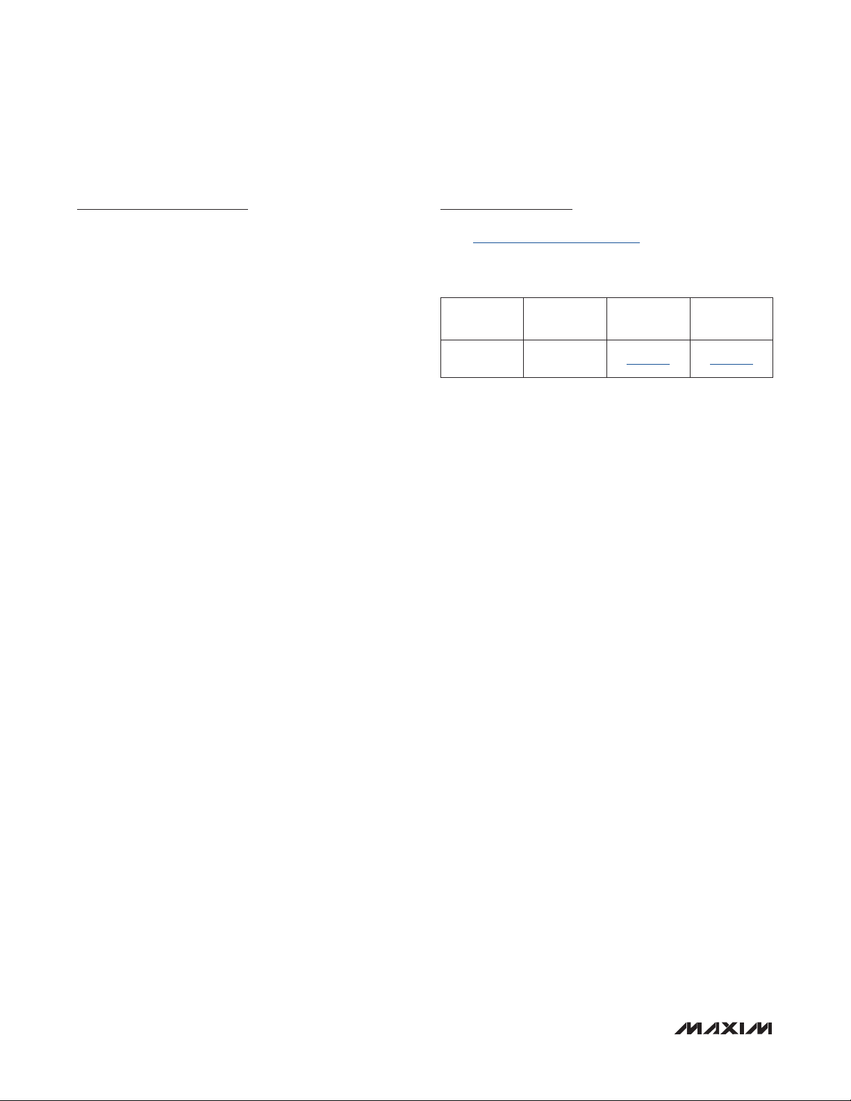
Pin Configuration
TOP VIEW
V
CC
6 5 4
MAX2666
MAX2668
1 2 3
LNA_IN LNA_GNDBIAS_GND
ULTRA-THIN LGA
LNA_OUT/
GAIN0GAIN1
MAX2666/MAX2668
Pin Description
PIN NAME FUNCTION
1 LNA_IN RF Input. Match according to band in Table 1.
2 BIAS_GND DC and Bias Ground
3 LNA_GND RF Ground
4 LNA_OUT/GAIN0
5 GAIN1
6 V
CC
RF Output and Gain Control. Internally match to 50I. Couple gain logic with a 20kI
resistor. When DC is open-circuit, pin self-biases to logic-high.
Gain Control. Together with GAIN0, selects gain mode. Must be connected to
logic-high or logic-low.
Supply Voltage. Bypass with a 1000pF capacitor to ground.
6 ______________________________________________________________________________________

Tiny Low-Noise Amplifiers for HSPA/LTE
Detailed Description
The MAX2666/MAX2668 are low-power LNAs designed
for 3G mobile applications. The devices feature low
noise, high linearity, and three gain steps in a tiny plastic
package.
Input and Output Matching
The devices require one matching inductor at the input
port in series with a DC-blocking capacitor to achieve
optimal performance in NF, gain, IIP3, and phase shift.
Table 1 presents the recommended input-matching
network values. The output port is internally matched to
50I, eliminating the need for external matching components. At the output port, an external DC-blocking
capacitor should be used to isolate the control function
of the output pin.
DC Decoupling and Layout
A properly designed PCB is essential to any RF microwave circuit. Use controlled-impedance lines on all
high-frequency inputs and outputs. Bypass VCC with a
decoupling capacitor located close to the device.
For long VCC lines, it might be necessary to add decoupling capacitors. Locate these additional capacitors
further away from the device package. Proper grounding
of the GND pins is essential. If the PCB uses a top-side
MAX2666/MAX2668
RF ground, connect it directly to the GND pins. For a
board where the ground is not on the component layer,
connect the GND pins to the board with multiple vias
close to the package.
Gain Control
The devices’ LNA_OUT/GAIN0 pin is also used as a
control pin for the LNA gain modes according to the gain
control table. GAIN0 logic level is set through an external
20kI resistor. An external DC-blocking capacitor should
be used to isolate the control function of this dual-purpose pin (see the Typical Operating Circuit). The GAIN1
pin must be set to either logic-high or logic-low.
Refer to www.maxim-ic.com for the MAX2666/MAX2668
Evaluation Kit schematic, Gerber data, PADS layout file,
and BOM information.
Table 1. Matching Component Values in
Different Bands
BAND SERIES C (nF) SERIES L (nH)
1, 4, 10 10 3.9
5, 6 10 12
8 10 12
Detailed Application Circuit in EV Kit
V
CC
RFIN
C1
0.01µF
10%
(0402)
C4
0.01µF
10%
(0201)
3.9nH
Q0.1nH (MAX2666)
Q0.2nH (MAX2668)
12nH
(0402)
L4
1
2
LNA_IN
BIAS_GND
U1
V
GAIN1
6
CC
5
MAX2666
OPEN
(0201)
C7
3
LNA_GND
MAX2668
LNA_OUT/GAIN0
4
_______________________________________________________________________________________ 7
R1
I
0
(0201)
R2
0
I
(0201)
C5
1000pF
10%
(0402)
GND
GAIN1 GAIN0
20k
(0201)
0.01µF
(0201)
R4
I
C3
10%
RFOUT
Tiny Low-Noise Amplifiers for HSPA/LTE
Chip Information
PROCESS: SiGe BiCMOS
MAX2666/MAX2668
Package Information
For the latest package outline information and land patterns,
go to www.maxim-ic.com/packages. Note that a “+”, “#”, or
“-” in the package code indicates RoHS status only. Package
drawings may show a different suffix character, but the drawing
pertains to the package regardless of RoHS status.
PACKAGE
TYPE
6 Ultra-Thin
LGA
PACKAGE
CODE
Y61A1+2
OUTLINE
NO.
21-0190 90-0233
LAND
PATTERN NO.
8 ______________________________________________________________________________________

Tiny Low-Noise Amplifiers for HSPA/LTE
Revision History
MAX2666/MAX2668
REVISION
NUMBER
0 8/10 Initial release —
REVISION
DATE
DESCRIPTION
PAGES
CHANGED
Maxim cannot assume responsibility for use of any circuitry other than circuitry entirely embodied in a Maxim product. No circuit patent licenses are implied.
Maxim reserves the right to change the circuitry and specifications without notice at any time.
Maxim Integrated Products, 120 San Gabriel Drive, Sunnyvale, CA 94086 408-737-7600 9
©
2010 Maxim Integrated Products Maxim is a registered trademark of Maxim Integrated Products, Inc.
 Loading...