

Page 1
EVALUATION KIT
AVAILABLE
MAX2644
2.4GHz SiGe,
High IP3 Low-Noise Amplifier
________________________________________________________________ Maxim Integrated Products 1
19-1786; Rev 1; 11/03
For pricing, delivery, and ordering information, please contact Maxim/Dallas Direct! at
1-888-629-4642, or visit Maxim’s website at www.maxim-ic.com.
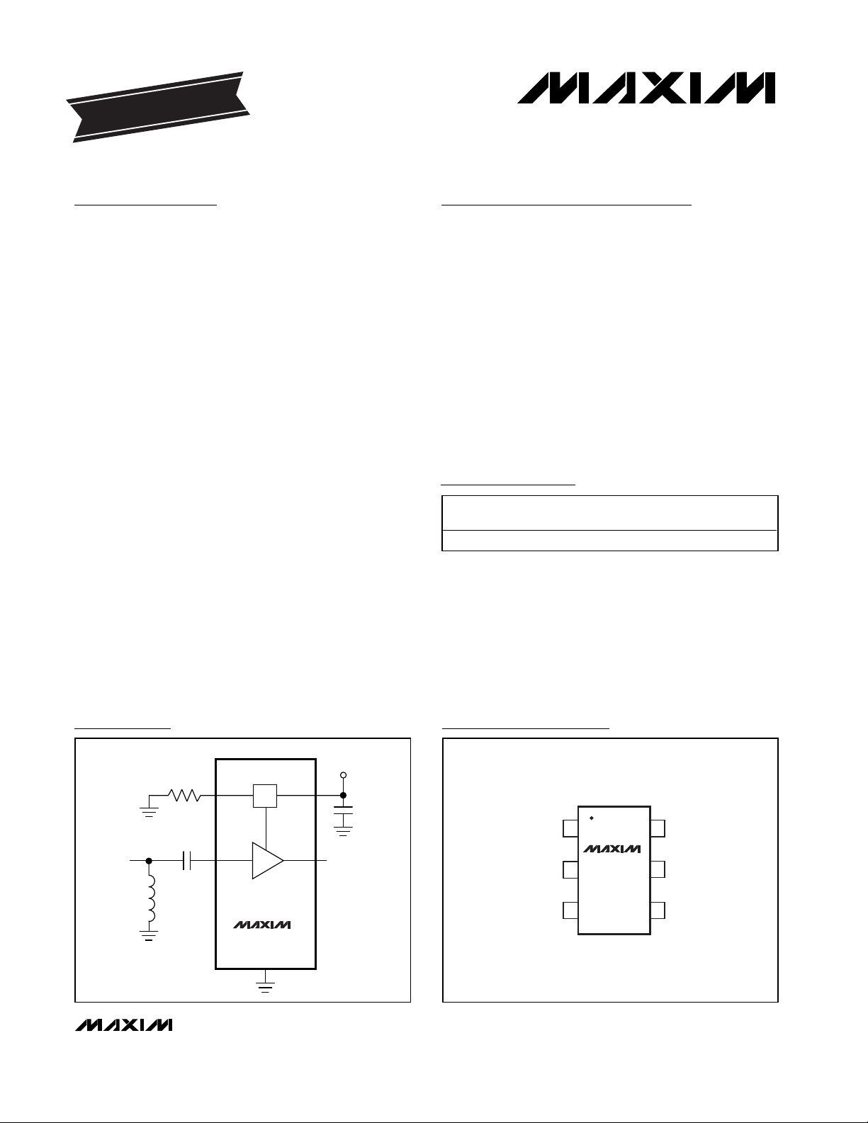
GND
V
CC
RFIN
16RFOUT
5 GND
BIAS
MAX2644
SC70-6
TOP VIEW
2
34
Pin Configuration
MAX2644
GND
BIAS
R
BIAS
1.2kΩ
RF OUTPUTRF INPUT
V
CC
V
CC
RFOUTRFIN
C1
33pF
L1
3.3nH
BIAS
Typical Operating Circuit
General Description
The MAX2644 low-cost, high third-order intercept point
(IP3) low-noise amplifier (LNA) is designed for applications in 2.4GHz WLAN, ISM, and Bluetooth radio systems. It features a programmable bias, allowing the
input IP3 and supply current to be optimized for specific applications. The LNA provides up to +1dBm input
IP3 while maintaining a low noise figure of 2.0dB and a
typical gain of 16dB.
The MAX2644 is designed on a low-noise, advanced
silicon-germanium (SiGe) technology. It operates with a
+2.7V to +5.5V single supply and is available in an
ultra-small 6-pin SC70 package.
________________________Applications
Bluetooth
802.11 WLAN
Home RF
Satellite CD Radio
2.4GHz ISM Band Radios
2.4GHz Cordless Phones
Wireless Local Loop (WLL)
Features
♦ Low Noise Figure (2.0dB at 2450MHz)
♦ High Gain: 16dB
♦ Adjustable IP3 and Bias Current
♦ Low-Power Standby Mode
♦ On-Chip Output Matching
♦ +2.7V to +5.5V Single-Supply Operation
♦ Ultra-Small 6-Pin SC70 Package
Ordering Information
PART TEMP RANGE
MAX2644EXT-T -40°C to +85°C 6 SC70 AAG
PINPACKAGE
MARK
TOP
Page 2
MAX2644
2.4GHz SiGe,
High IP3 Low-Noise Amplifier
2 _______________________________________________________________________________________
ABSOLUTE MAXIMUM RATINGS
DC ELECTRICAL CHARACTERISTICS
(VCC= +2.7V to +5.5V, R
BIAS
= 1.2kΩ, no RF signal applied, R
FIN
and R
FOUT
are AC-coupled and terminated to 50Ω, TA= -40°C to
+85°C. Typical values are at V
CC
= +3.0V, TA= +25 °C, unless otherwise noted.) (Note 1)
Stresses beyond those listed under “Absolute Maximum Ratings” may cause permanent damage to the device. These are stress ratings only, and functional
operation of the device at these or any other conditions beyond those indicated in the operational sections of the specifications is not implied. Exposure to
absolute maximum rating conditions for extended periods may affect device reliability.
Note 1: Devices are production tested at TA= +25°C. Minimum and maximum values are guaranteed by design and characterization
over temperature and supply voltages.
Note 2: Min/Max limits are guaranteed by design and characterization.
Note 3: The part has been characterized at the specified frequency range. Operation outside this range is possible but not guaranteed.
Note 4: Excluding PC board losses (0.3dB at the input and 0.3dB at the output of the MAX2644 EV kit).
Note 5: Measured with two input tones (f
1
= 2445MHz, f2= 2455MHz) both at -30dBm per tone. Input IP3 can be improved to
+1dBm with circuit shown in Figure 2.
Note 6: Excluding PC board losses (0.3dB typical at the input of the MAX2644 EV kit).
V
CC
to GND ..............................................................-0.3V to +6V
RFIN, RFOUT to GND…......................................................±0.3V
RFIN Power (50Ω source) ................................................+5dBm
BIAS to GND ................................................................0 to +0.3V
Operating Temperature Range ...........................-40°C to +85°C
Maximum Junction Temperature .....................................+150°C
Continuous Power Dissipation (T
A
= +70°C)
6-Pin SC70 (derate 3.1mW/°C above +70°C)..............245mW
Storage Temperature.........................................-65°C to +150°C
Lead Temperature (soldering, 10s) .................................+300°C
AC ELECTRICAL CHARACTERISTICS
(MAX2644 EV kit, VCC= +3.0V, f
RFIN
= 2450MHz, P
RFIN
= -30dBm, input and output are terminated to 50Ω, R
BIAS
= 1.2kΩ,
T
A
= +25°C, unless otherwise noted.) (Note 2)
Supply Voltage 2.7 5.5 V
Operating Supply Current
Standby Supply Current R
PARAMETER CONDITIONS MIN TYP MAX UNITS
R
= 3.9kΩ 2.7
BIAS
R
= 1.2kΩ, TA = +25°C 7.0 9.7
BIAS
R
= 1.2kΩ, TA = -40°C to +85°C 11.0
BIAS
R
= 750Ω 10.2
BIAS
is unconnected, TA = +25°C, VCC = 3.3V 100 µA
BIAS
mA
Operating Frequency (Note 3) 2400 2500 MHz
Gain (Note 4) 15 17 dB
Gain Variation Over Temperature TA = -40°C to +85°C ±0.7 ±1.0 dB
Input Third-Order Intercept Point
(Note 5)
Input 1dB Compression Point -13 dBm
Noise Figure (Note 6) 2.0 2.5 dB
Input Return Loss -15 dB
Output Return Loss -10 dB
Reverse Isolation -30 dB
PARAMETER CONDITIONS MIN TYP MAX UNITS
R
= 750Ω -4
BIAS
RBIAS = 1.2kΩ
BIAS = 3.9kΩ
R
-3
-8
dBm
Page 3
MAX2644
2.4GHz SiGe,
High IP3 Low-Noise Amplifier
_______________________________________________________________________________________ 3
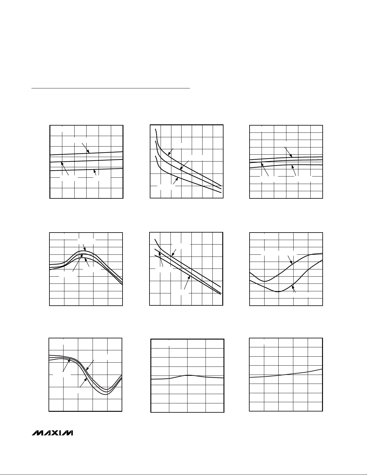
Typical Operating Characteristics
(P
RFIN
= -30dBm, ZS= ZL= 50Ω, VCC= +3.0V, f
RFIN
= 2450MHz, R
BIAS
= 1.2kΩ, TA= +25°C, unless otherwise noted.)
0
4
2
8
6
12
10
14
2.5 3.5 4.03.0 4.5 5.0 5.5
SUPPLY CURRENT vs. SUPPLY VOLTAGE
MAX2644 toc01
SUPPLY VOLTAGE (V)
SUPPLY CURRENT (mA)
TA = +25°C
TA = -40°C
TA = +85°C
R
BIAS
= 1.2kΩ
13
15
14
17
16
18
19
0.5 2.0 2.51.0 1.5 3.0 3.5 4.0
GAIN vs. R
BIAS
MAX2644 toc05
R
BIAS
(kΩ)
GAIN (dB)
TA = -40°C
TA = +85°C
TA = +25°C
-20
-14
-16
-18
-12
-10
-8
-6
-4
-2
0
2200 24002300 2500 2600 2700
INPUT AND OUTPUT RETURN LOSS
vs. FREQUENCY
MAX2644 toc06
FREQUENCY (MHz)
REVERSE ISOLATION (dB)
OUTPUT RETURN LOSS
R
BIAS
= 1.2kΩ
INPUT RETURN LOSS
0
0.5
1.0
1.5
2.0
2.5
3.0
3.5
4.0
2350 2400 2450 2500 2550
NOISE FIGURE vs. FREQUENCY
MAX2644 toc08
FREQUENCY (MHz)
NOSIE FIGURE (dB)
R
BIAS
= 1.2kΩ
0
0.5
1.0
1.5
2.0
2.5
3.0
3.5
4.0
-40 -15 10 35 60 85
NOISE FIGURE vs. TEMPERATURE
MAX2644 toc09
TEMPERATURE (°C)
NOSIE FIGURE (dB)
R
BIAS
= 1.2kΩ
10
13
12
11
14
15
16
17
18
19
20
2200 24002300 2500 2600 2700
GAIN vs. FREQUENCY
MAX2644 toc04
FREQUENCY (MHz)
GAIN (dB)
TA = -40°C
TA = +85°C
TA = +25°C
R
BIAS
= 1.2kΩ
-50
-40
-45
-30
-35
-25
-20
2200 24002300 2500 2600 2700
REVERSE ISOLATION vs. FREQUENCY
MAX2644 toc07
FREQUENCY (MHz)
REVERSE ISOLATION (dB)
TA = +25°C
TA = +85°C
R
BIAS
= 1.2kΩ
TA = -40°C
1
5
3
9
7
11
13
0.5 2.0 2.51.0 1.5 3.0 3.5 4.0
SUPPLY CURRENT vs. R
BIAS
MAX2644 toc02
R
BIAS
(kΩ)
SUPPLY CURRENT (mA)
TA = +25°C
TA = +85°C
TA = -40°C
12
15
14
13
16
17
18
19
20
21
22
2.5 3.53.0 4.0 4.5 5.0 5.5
GAIN vs. SUPPLY VOLTAGE
MAX2644 toc03
SUPPLY VOLTAGE (V)
GAIN (dB)
TA = +25°C
R
BIAS
= 1.2kΩ
TA = +85°C
TA = -40°C
Page 4
MAX2644
2.4GHz SiGe,
High IP3 Low-Noise Amplifier
4 _______________________________________________________________________________________
Pin Description
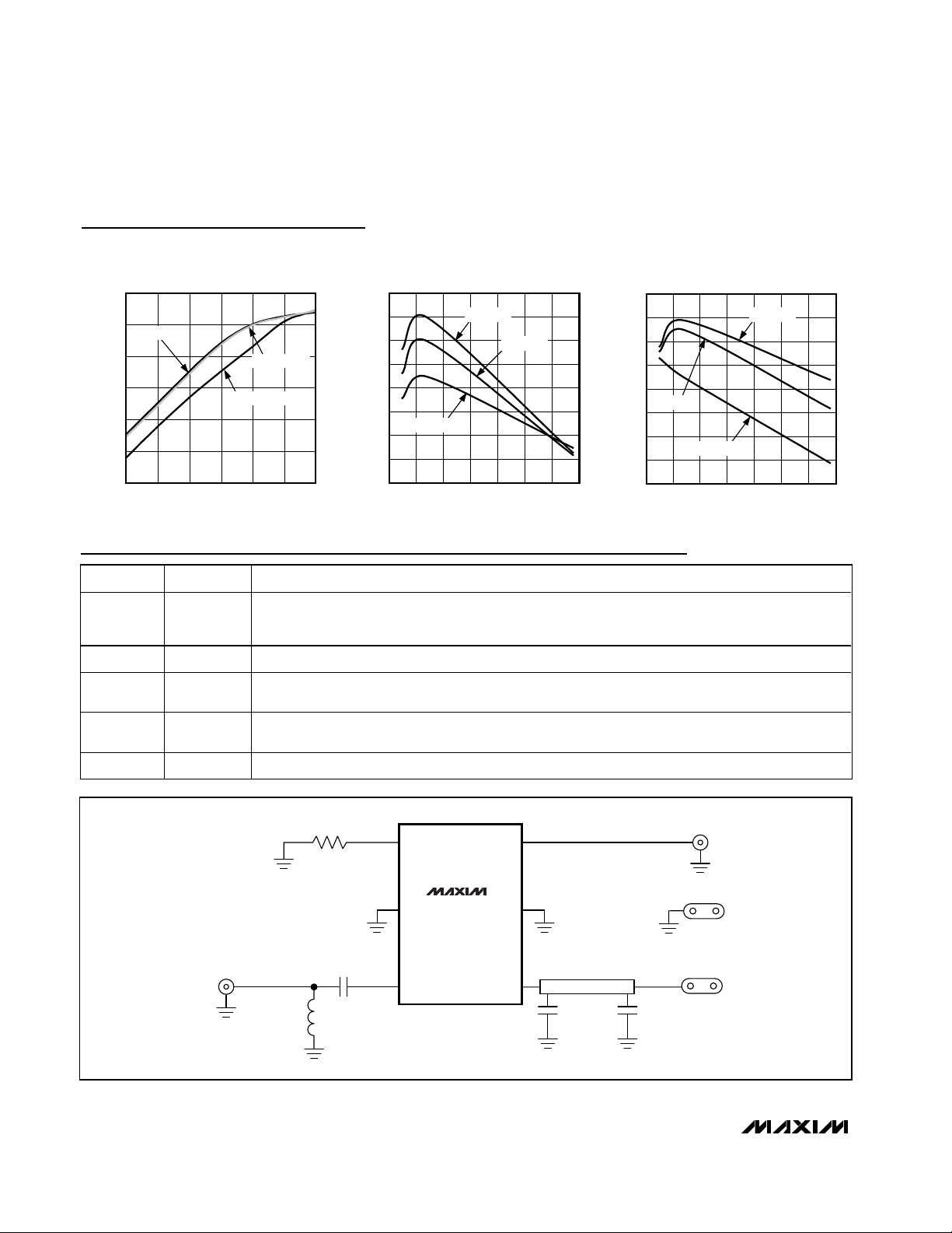
Typical Operating Characteristics (continued)
(P
RFIN
= -30dBm, ZS= ZL= 50Ω, VCC= +3.0V, f
RFIN
= 2450MHz, R
BIAS
= 1.2kΩ, TA= +25°C, unless otherwise noted.)
-20
-10
-15
0
-5
5
10
-30 -20 -15-25 -10 -5 0
OUTPUT POWER vs. INPUT POWER
MAX2644 toc10
INPUT POWER (dBm)
OUTPUT POWER (dBm)
R
BIAS
= 750Ω
R
BIAS
= 1.2kΩ
R
BIAS
= 3.9kΩ
IIP3 vs. R
BIAS
MAX2644 toc11
-9
-8
-6
-7
-3
-2
-4
-5
-1
IIP3 (dBm)
0.5 1.5 2.01.0
2.5
3.0 3.5 4.0
R
BIAS
(kΩ)
TA = +85°C
TA = +25°C
TA = -40°C
INPUT P
1dB
vs. R
BIAS
MAX2644 toc12
-19
-18
-16
-17
-13
-12
-14
-15
-11
INPUT P
1dB
(dBm)
0.5 1.5 2.01.0
2.5
3.0 3.5 4.0
R
BIAS
(kΩ)
TA = +85°C
TA = -40°C
TA = +25°C
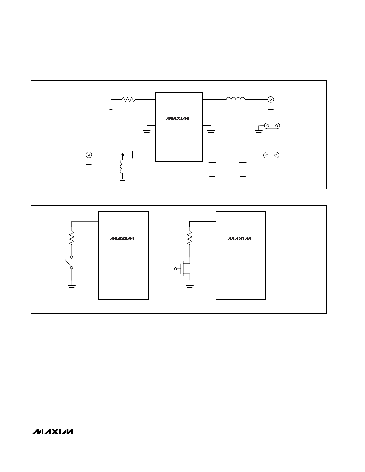
Figure 1. High Gain Design
PIN NAME DESCRIPTION
1 BIAS
2, 5 GND Ground. For optimum performance, provide a low-inductance connection to the ground plane.
3 RFIN
4V
6 RFOUT Amplifier Output. AC-coupled internally.
CC
RFIN
SMA
GAIN: 17dB
IIP3: -3dBm
Resistor Bias Control. Connect a resistor, R
, from BIAS to ground. R
BIAS
current. The current through this pin is approximately 60mV divided by R
Information).
Amplifier Input. AC-couple to this pin with a DC blocking capacitor. External matching network is
required for optimum performance.
Supply Voltage. Bypass with a capacitor directly to ground at the supply pin. Refer to V
Bypassing section for more information.
6
RFOUTBIAS
5
GND
Length = 400mils
4
V
CC
C3
2.2pF
C2
33pF
3.3nH
1
R1
1.2kΩ
2
GND
C1
33pF
L1
3
RFIN
U1
MAX2644
sets IP3 and supply
BIAS
(see Applications
BIAS
RFOUT
SMA
GND
VCC
CC
Line
Page 5
MAX2644
2.4GHz SiGe,
High IP3 Low-Noise Amplifier
_______________________________________________________________________________________ 5
Applications Information
Input Matching
Input matching is required for optimum performance.
The MAX2644 requires a simple LC matching network,
as shown in the Typical Operating Circuit. To further
reduce cost and external component count, replace the
external inductor with a microstrip transmission line.
The Typical Operating Circuit shows the recommended
input matching network for the MAX2644 at 2450MHz.
These values are optimized for best simultaneous gain,
noise figure, and return loss performance.
VCCLine Bypassing
Bypassing the VCCline is necessary for optimum
gain/linearity performance. A transmission line and two
capacitors are required, as shown in the schematics in
Figures 1 and 2. The optimum dimensions and positions of the components are as follows: the output
transmission line dimension is 0.532in (length) ✕ 0.012in
(width); the distance from C2 to the IC is 0.352in; and
the distance from C3 to the IC is 0.041in. Please refer
to Figures 1 and 2 for component values.
Figure 2. High Linearity Design
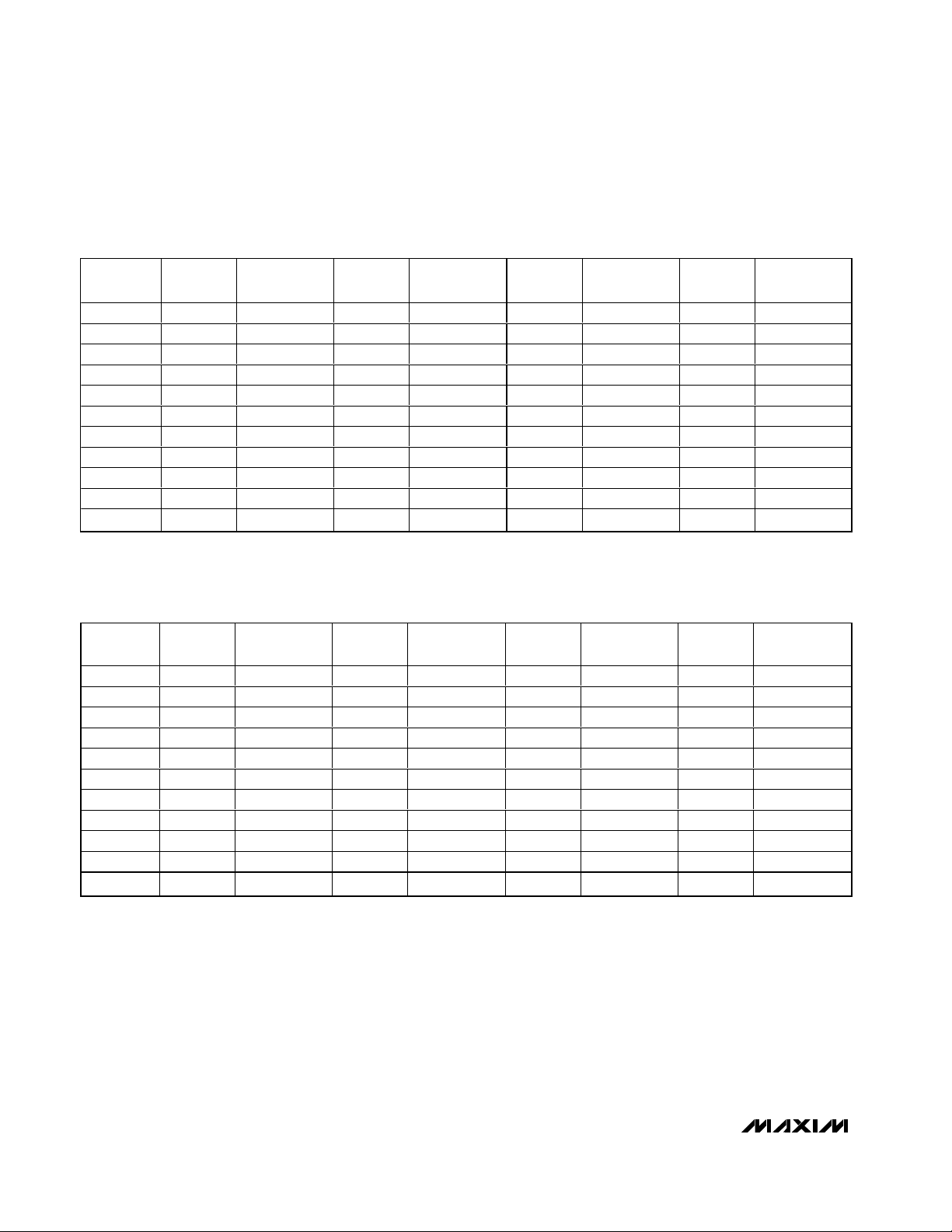
Figure 3. Recommended MAX2644 Standby Configurations
RFIN
SMA
GAIN: 16dB
IIP3: +1dBm
1
R1
1.2kΩ
2
GND
C1
33pF
L1
3.3nH
BIAS BIAS
MAX2644 MAX2644
3
RFIN
U1
MAX2644
6
RFOUTBIAS
5
GND
Length = 400mils
4
V
CC
C3
15pF
L2
3.9nH
C2
33pF
RFOUT
GND
V
CC
SMA
(a) (b)
Page 6
MAX2644
Standby
Standby mode is achieved by disconnecting BIAS as
shown in Figure 1. Avoid capacitance at the BIAS pin
by connecting the bias resistor from BIAS to the switch.
Layout Issues
A properly designed PC board is essential to any
RF/microwave circuit. Use controlled impedance lines
on all high-frequency inputs and outputs. Bypass with
decoupling capacitors located close to the device V
CC
pin. For long VCClines, it may be necessary to add
additional decoupling capacitors. These additional
capacitors can be located farther away from the device
package. Proper grounding of the GND pins is essential. If the PC board uses a topside RF ground, connect
it directly to all GND pins. For a board where the
ground plane is not on the component layer, the best
technique is to connect the GND pins to the board with
a plated through-hole located close to the package.
2.4GHz SiGe,
High IP3 Low-Noise Amplifier
6 _______________________________________________________________________________________
Table 1. MAX2644 Typical Scattering Parameters
(R
BIAS
= 750Ω, VCC= +3.0V, TA= +25°C.)
Table 2. MAX2644 Typical Scattering Parameters
(R
BIAS
= 1.2kΩ, VCC= +3.0V, TA= +25°C.)
FREQ.
(MHz)
2200 0.3372 -79.36 5.1940 170.97 0.0414 157.19 0.2818 -73.71
2250 0.3098 -70.09 5.3156 166.79 0.0445 146.70 0.2204 -67.13
2300 0.3283 -57.20 5.4281 159.22 0.0469 130.62 0.1566 -50.26
2350 0.4005 -50.46 5.4175 150.70 0.0441 108.72 0.1480 -3.96
2400 0.4839 -50.28 5.3346 143.93 0.0349 85.67 0.2795 15.12
2450 0.5443 -56.33 5.0687 136.45 0.0233 58.80 0.4179 11.12
2500 0.5758 -60.09 4.9556 132.16 0.0113 27.74 0.5135 3.28
2550 0.5784 -63.61 4.5952 127.68 0.0041 -38.98 0.5622 -2.66
2600 0.5698 -66.56 4.2364 126.58 0.0063 -110.49 0.5986 -7.45
2650 0.5600 -68.51 4.1376 126.51 0.0103 -128.93 0.6208 -10.43
2700 0.5533 -69.86 4.0729 120.60 0.0133 -140.21 0.6425 -12.93
FREQ.
(MHz)
2200 0.3482 -67.06 5.2390 -177.33 0.0402 161.53 0.2873 -76.58
2250 0.3121 -58.60 5.3790 178.72 0.0435 151.97 0.2305 -69.42
2300 0.3051 -43.64 5.5982 173.43 0.0452 136.90 0.1735 -54.22
2350 0.3693 -30.34 5.8137 166.48 0.0427 116.57 0.1582 -16.42
2400 0.4769 -29.48 5.8063 158.29 0.0341 95.13 0.2687 6.52
2450 0.5619 -35.54 5.6624 150.06 0.0236 68.36 0.4043 5.00
2500 0.5948 -42.64 5.3015 142.37 0.0117 41.34 0.5030 -2.19
2550 0.5939 -47.58 4.7813 136.67 0.0034 -13.74 0.5602 -8.04
2600 0.5825 -50.94 4.3271 134.58 0.0056 -104.09 0.5952 -12.76
2650 0.5708 -53.14 4.1961 133.48 0.0096 -124.80 0.6215 -15.97
2700 0.5604 -54.35 4.1068 128.01 0.0125 -134.75 0.6434 -18.83
S11
MAG
S11
MAG
S11 PHASE
(DEGREES)
S11 PHASE
(DEGREES)
S21
MAG
S21
MAG
S21 PHASE
(DEGREES)
S21 PHASE
(DEGREES)
S12
MAG
S12
MAG
S12 PHASE
(DEGREES)
S12 PHASE
(DEGREES)
S22
MAG
S22
MAG
S22 PHASE
(DEGREES)
S22 PHASE
(DEGREES)
Page 7
MAX2644
2.4GHz SiGe,
High IP3 Low-Noise Amplifier
_______________________________________________________________________________________ 7
Table 3. MAX2644 Typical Scattering Parameters
(R
BIAS
= 3.9kΩ, VCC= +3.0V, TA= +25°C.)
Table 4. MAX2644 Typical Noise
Parameters at V
CC
= +3.0V, TA= +25°C,
R
BIAS
= 750Ω
Table 5. MAX2644 Typical Noise
Parameters at VCC= +3.0V, TA= +25°C,
R
BIAS
= 1.2kΩ
Table 6. MAX2644 Typical Noise
Parameters at V
CC
= +3.0V, TA= +25°C,
R
BIAS
= 3.9kΩ
Chip Information
TRANSISTOR COUNT: 87
FREQUENCY
FREQ.
(MHz)
2200 0.4894 -75.32 3.7368 -173.73 0.0348 156.35 0.2729 -62.97
2250 0.4566 -72.73 3.7718 -177.51 0.0363 147.30 0.2459 -53.68
2300 0.4335 -68.17 3.8855 177.43 0.0369 132.32 0.2211 -41.12
2350 0.4343 -61.46 3.9783 171.34 0.0344 116.21 0.2177 -21.15
2400 0.4695 -57.00 4.0230 165.15 0.0272 95.31 0.2823 -2.41
2450 0.5156 -57.52 4.0087 157.68 0.0179 70.07 0.3924 1.25
2500 0.5403 -61.04 3.8380 149.58 0.0079 42.40 0.4849 -2.71
2550 0.5423 -63.93 3.5140 143.30 0.0018 -46.47 0.5476 -7.30
2600 0.5361 -66.30 3.2048 140.25 0.0055 -112.91 0.5881 -11.35
2650 0.5280 -68.08 3.1204 138.55 0.0100 -132.25 0.6170 -14.57
2700 0.5217 -69.29 3.0860 132.16 0.0121 -133.97 0.6418 -17.44
S11
MAG
S11 PHASE
(DEGREES)
S21
MAG
S21 PHASE
(DEGREES)
S12
MAG
S12 PHASE
(DEGREES)
S22
MAG
F
(MHz)
2400 1.725 0.361 66.13 24.38
2450 1.747 0.360 66.93 24.76
2500 1.769 0.358 67.72 25.14
MIN
(dB)
Γ
opt
Γ
opt
ANGLE
R
(Ω)
N
FREQUENCY
(MHz)
2400 1.570 0.409 69.84 21.77
2450 1.589 0.408 70.63 21.94
2500 1.609 0.406 71.63 22.42
F
MIN
(dB)
Γ
Γ
opt
opt
ANGLE
S22 PHASE
(DEGREES)
R
N
(Ω)
FREQUENCY
(MHz)
2400 1.497 0.510 86.55 20.58
2450 1.517 0.507 86.50 20.90
2500 1.538 0.504 88.18 21.25
F
(dB)
MIN
Γ
opt
Γ
opt
ANGLE
R
(Ω)
N
Page 8

MAX2644
2.4GHz SiGe,
High IP3 Low-Noise Amplifier
Maxim cannot assume responsibility for use of any circuitry other than circuitry entirely embodied in a Maxim product. No circuit patent licenses are
implied. Maxim reserves the right to change the circuitry and specifications without notice at any time.
8 _____________________Maxim Integrated Products, 120 San Gabriel Drive, Sunnyvale, CA 94086 408-737-7600
© 2003 Maxim Integrated Products Printed USA is a registered trademark of Maxim Integrated Products.
Package Information (continued)
(The package drawing(s) in this data sheet may not reflect the most current specifications. For the latest package outline information
go to www.maxim-ic.com/packages
.)
SC70, 6L.EPS
 Loading...