

Page 1
General Description
The MAX2634 low-noise amplifier (LNA) with low-power
shutdown mode is optimized for 315MHz and
433.92MHz automotive remote keyless entry (RKE)
applications. At 315MHz, the LNA achieves 15.5dB
power gain and a 1.25dB noise figure while only consuming 2.5mA of supply current from a 2.2V to 5.5V
power supply. An integrated logic-controlled low-power
shutdown mode reduces power consumption to 0.1µA
and replaces the two transistors typically required to
implement the shutdown function in discrete-based
RKE LNA solutions. The device further reduces component count by integrating the output matching and DCblocking components, and only requires a single
inductor to match the input for best noise figure and
input return loss.
The device is available in a small 6-pin (2.0mm x
2.2mm x 0.9mm) lead-free SC70 package for automotive applications that require visual inspection of PCB
solder connections.
Applications
Remote Keyless Entry (RKE)
Tire Pressure Monitoring Systems (TPMS)
Security
Garage Door Openers
Telemetry Receivers
Features
o Optimized for 308MHz, 315MHz, 418MHz,
and 433.92MHz
o 2.2V to 5.5V Supply Voltage Range
o Low Operating Supply Current
2.5mA (typ), 4mA (max)
o Logic-Controlled 1µA (max) Shutdown
o Typical Performance at 315MHz
1.25dB Noise Figure
-16dBm Input IP3
15.5dB Power Gain
o Automotive Temperature Range
-40°C to +125°C
o ESD Rating of ±2.5kV (HBM) on All Pins
o AEC-Q100 Qualification
MAX2634
315MHz/433MHz Low-Noise
Amplifier for Automotive RKE
________________________________________________________________
Maxim Integrated Products
1
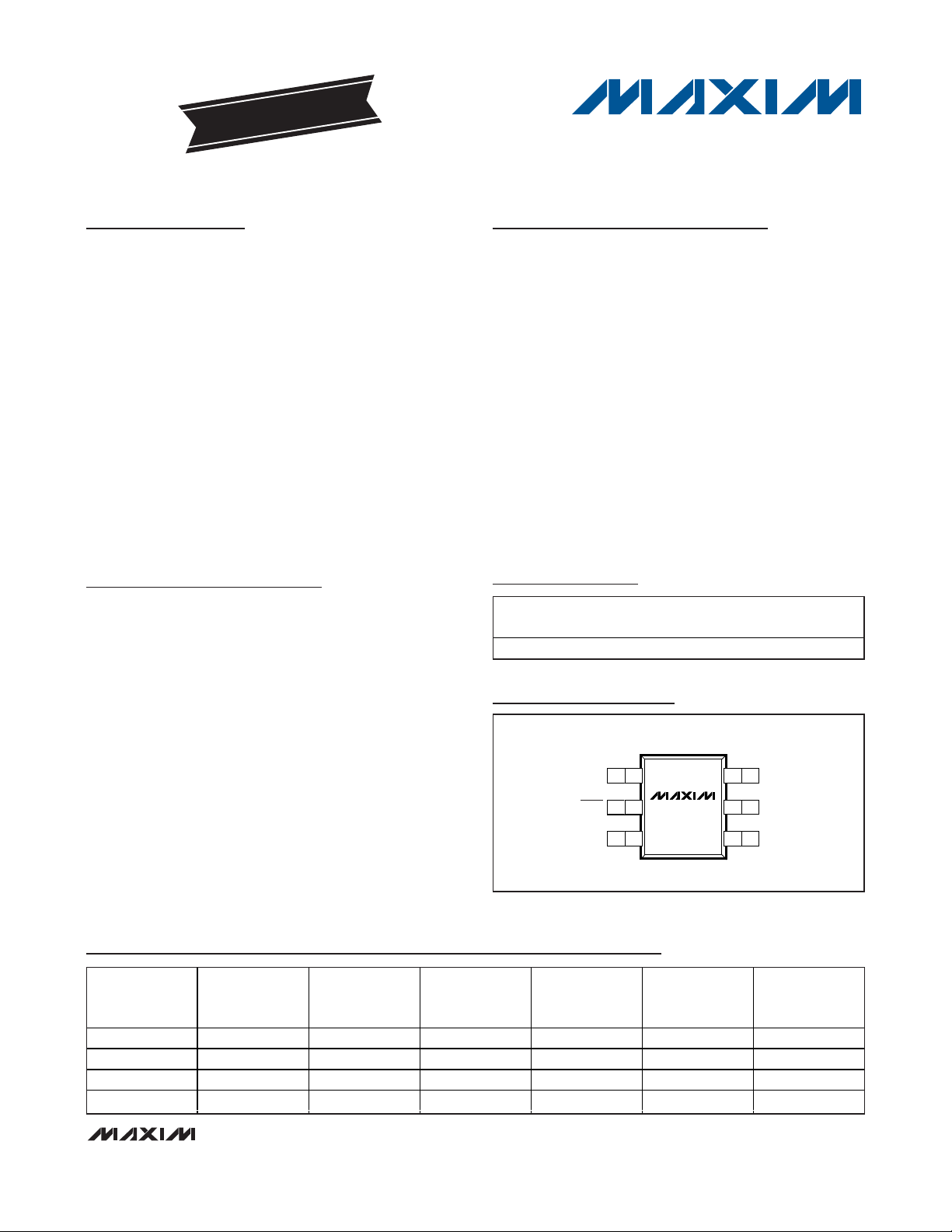
Pin Configuration
Performance Table
19-4383; Rev 1; 3/09
For pricing, delivery, and ordering information, please contact Maxim Direct at 1-888-629-4642,
or visit Maxim’s website at www.maxim-ic.com.
EVALUATION KIT
AVAILABLE
FREQUENCY
(MHz)
L1
(nH)
SUPPLY
CURRENT
(mA)
GAIN
(dB)
NOISE FIGURE
(dB)
INPUT P1dB
(dBm)
INPUT IP3
(dBm)
308 56 2.5 15.5 1.25 -29 -16
315 56 2.5 15.5 1.25 -29 -16
418 33 2.5 13.5 1.25 -26 -12
433.92 33 2.5 13.5 1.25 -26 -12
Functional Diagram/Typical Operating Circuit appears at
end of data sheet.
+
Denotes a lead(Pb)-free/RoHS-compliant package.
PART
TEMP RANGE
PIN-
TOP
MARK
6 SC70
+ADG
Ordering Information
PACKAGE
MAX2634AXT+ -40°C to +125°C
TOP VIEW
GND
SHDN
GND
+
1
2
MAX2634
3
6
RFOUT
5
V
CC
4
RFIN
SC70
Page 2
MAX2634
315MHz/433MHz Low-Noise
Amplifier for Automotive RKE
2 _______________________________________________________________________________________
ABSOLUTE MAXIMUM RATINGS
DC ELECTRICAL CHARACTERISTICS
(VCC= +2.2V to +5.5V, TA= -40°C to +125°C, Typical values are at VCC= +3.0V, TA= +25°C, unless otherwise noted. RFIN and
RFOUT are AC-coupled and terminated to 50Ω. No RF input signals at RFIN and RFOUT.) (Note 2)
Stresses beyond those listed under “Absolute Maximum Ratings” may cause permanent damage to the device. These are stress ratings only, and functional
operation of the device at these or any other conditions beyond those indicated in the operational sections of the specifications is not implied. Exposure to
absolute maximum rating conditions for extended periods may affect device reliability.
VCCPin to GND.....................................................-0.3V to +6.0V
RFIN.................Pin Must Be AC-Coupled with DC-Blocking Cap
RFOUT, SHDN............................................-0.3V to (V
CC
+ 0.3V)
RF Input Power .................................................................+5dBm
Continuous Power Dissipation (T
A
= +70°C)
6-Pin SC70 (derate 3.1mW/°C above +70°C)..............245mW
Junction-to-Case Thermal Resistance (θ
JC
)
(Note 1) ......................................................................115°C/W
Junction-to-Ambient Thermal Resistance (θ
JA
)
(Note 1) ......................................................................326°C/W
Operating Temperature Range .........................-40°C to +125°C
Junction Temperature......................................................+150°C
Storage Temperature Range .............................-65°C to +160°C
Lead Temperature (soldering, 10s)....................................300°C
Note 1: Package thermal resistances were obtained using the method described in JEDEC specification JESD51-7, using a 4-layer
board. For detailed information on package thermal considerations, refer to www.maxim-ic.com/thermal-tutorial
.
CAUTION! ESD SENSITIVE DEVICE
PARAMETER CONDITIONS MIN TYP MAX UNITS
Operating Supply Voltage 2.2 5.5 V
Operating Supply Current
Shutdown Supply Current
DIGITAL CONTROL INPUTS (SHDN)
Digital Input-Voltage High 1.1 V
Digital Input-Voltage Low 0.4 V
Digital Input-Current High V
Digital Input-Current Low V
SHUTDOWN MODE CONTROL
Enable Time 130 µs
Disable Time 20 µs
SHDN = high, TA = +25°C 2.5 4 mA
SHDN = high, T
V
= 0, TA = +25°C1µA
SHDN
= 0, TA = -40°C to +125°C10µA
V
SHDN
= V
SHDN
= V
SHDN
= -40°C to +125°C6mA
A
IH
IL
5µA
1µA
Page 3
MAX2634
315MHz/433MHz Low-Noise
Amplifier for Automotive RKE
_______________________________________________________________________________________ 3
AC ELECTRICAL CHARACTERISTICS
(MAX2634 EV Kit, VCC= +2.2V to +5.5V, TA= -40°C to +125°C. Typical values are at VCC= +3.0V and TA= +25°C, unless otherwise
noted. P
RFIN
= -40dBm, SHDN = high.) (Note 2)
Note 2: Guaranteed by production test at T
A
= +25°C. Guaranteed by design and characterization at TA= -40°C and TA= +125°C.
Note 3: Measured with two tones located at 315MHz and 316MHz or 433MHz and 434MHz at -40dBm/tone.
Note 4: Guaranteed by design and characterization.
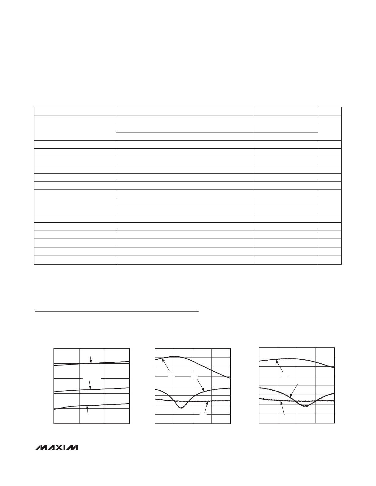
Typical Operating Characteristics
(MAX2634 EV Kit, VCC= +2.2V to +5.5V, TA= -40°C to +125°C. Typical values are at VCC= +3.0V and TA= +25°C, unless otherwise
noted. f
RFIN
= 315MHz/433MHz, P
RFIN
= -40dBm, SHDN = high.)
PARAMETER CONDITIONS MIN TYP MAX UNITS
f
= 315MHz
RFIN
Power Gain
TA = +25°C 12.5 15.5
= -40°C to +125°C, VCC = +3.0V 11.5
T
A
dB
Noise Figure TA = +25°C 1.25 dB
Input Third-Order Intercept Point (Note 3) -16 dBm
Input 1dB Compression Point -29 dBm
Input Return Loss 10 dB
Output Return Loss 8dB
Reverse Isolation 60 dB
f
= 433.92MHz
RFIN
Power Gain
TA = +25°C (Note 4) 11 13.5
= -40°C to +125°C, VCC = +3.0V (Note 4) 10
T
A
dB
Noise Figure TA = +25°C 1.25 dB
Input Third-Order Intercept Point (Note 3) -12 dBm
Input 1dB Compression Point -26 dBm
Input Return Loss 11 dB
Output Return Loss 8dB
Reverse Isolation 60 dB
SUPPLY CURRENT vs. SUPPLY VOLTAGE
4.0
3.5
3.0
2.5
SUPPLY CURRENT (mA)
2.0
1.5
2.2 3.3 4.4 5.5
TA = +125°C
TA = +25°C
TA = -40°C
SUPPLY VOLTAGE (V)
20
15
MAX2634 toc01
10
5
0
-5
S11, S22, S21 (dB)
-10
-15
-20
200 300 400 500 600
S11, S22, S21 vs. FREQUENCY
(315MHz)
S21
S11
S22
FREQUENCY (MHz)
MAX2634 toc02
S11, S22, S21 vs. FREQUENCY
(433MHz)
20
15
10
5
0
-5
S11, S22, S21 (dB)
-10
-15
-20
200 300 400 500 600
S21
S11
S22
FREQUENCY (MHz)
MAX2634 toc03
Page 4

MAX2634
315MHz/433MHz Low-Noise
Amplifier for Automotive RKE
4 _______________________________________________________________________________________
Typical Operating Characteristics (contineed)
(MAX2634 EV Kit, VCC= +2.2V to +5.5V, TA= -40°C to +125°C. Typical values are at VCC= +3.0V and TA= +25°C, unless otherwise
noted. f
RFIN
= 315MHz/433MHz, P
RFIN
= -40dBm, SHDN = high.)
IIP3 vs. SUPPLY VOLTAGE
-10
TA = +125°C
-12
-14
TA = +25°C
(315MHz)
-5
MAX2634 toc04
-8
-11
IIP3 vs. SUPPLY VOLTAGE
(433MHz)
TA = +125°C
TA = +25°C
MAX2634 toc05
NOISE FIGURE vs. SUPPLY VOLTAGE
(433MHz)
2.5
TA = +125°C
2.0
TA = +25°C
1.5
MAX2634 toc06
IIP3 (dBm)
-16
-18
-20
23456
TA = -40°C
SUPPLY VOLTAGE (V)
NOISE FIGURE vs. SUPPLY VOLTAGE
(315MHz)
2.5
2.0
1.5
1.0
NOISE FIGURE (dB)
0.5
0
23456
TA = +125°C
TA = +25°C
TA = -40°C
SUPPLY VOLTAGE (V)
TURN-ON TIME
-20
-30
f
= 315MHz
RFIN
-40
-50
-60
-70
-80
OUTPUT POWER (dBm)
-90
-100
-110
-120
= -43dBm
P
RFIN
1AVG
040608020 100 120 140 180160 200
TIME (µs)
MAX2634 toc07
IIP3 (dBm)
-14
-17
-20
23456
TA = -40°C
SUPPLY VOLTAGE (V)
GAIN vs. SUPPLY VOLTAGE
(433MHz)
17
16
15
14
GAIN (dB)
13
12
11
TA = +25°C
23456
SUPPLY VOLTAGE (V)
MAX2634 toc10
TA = -40°C
TA = +125°C
OUTPUT POWER (dBm)
-100
-110
-120
1.0
NOISE FIGURE (dB)
0.5
0
23456
SUPPLY VOLTAGE (V)
GAIN vs. SUPPLY VOLTAGE
17
TA = -40°C
16
MAX2634 toc08
15
14
GAIN (dB)
13
12
11
23456
SUPPLY VOLTAGE (V)
SHUTDOWN TIME
-20
-30
-40
-50
-60
-70
-80
-90
f
= 315MHz
RFIN
= -43dBm
P
RFIN
1AVG
01015205 253035 4540 50
TIME (µs)
TA = -40°C
(315MHz)
TA = +25°C
MAX2634 toc09
TA = +125°C
MAX2634 toc11
Page 5

MAX2634
315MHz/433MHz Low-Noise
Amplifier for Automotive RKE
_______________________________________________________________________________________ 5
Detailed Description
The MAX2634 LNA with low-power shutdown mode is
optimized for 308MHz, 315MHz, 418MHz, and 433MHz
automotive RKE applications, which are required to
operate over the -40°C to +125°C automotive temperature range. The device reduces component count by
integrating the output matching and DC-blocking components, and only requires a single inductor to match
the input for best noise figure and input return loss. An
integrated logic-controlled low-power shutdown mode
reduces power consumption to 0.1µA and replaces the
two transistors typically required to implement the shutdown function in discrete-based RKE LNA solutions.
Input Matching
The MAX2634 requires an off-chip input matching network. The
Functional Diagram/Typical Operating Circuit
shows the recommended input-matching network component values for operation at 315MHz and 433MHz.
These values are optimized for the best simultaneous
gain, noise figure, and return loss performance. Table 1
lists typical input and output impedances.
Pin Description
Table 1. Typical Input and Output Impedances in R+jX Format
(VCC= +3.0V, TA= +25°C.)
PIN NAME FUNCTION
1, 3 GND Ground. Use minimum path to ground plane to minimize inductance.
2 SHDN Shutdown Input. A logic-level high enables the LNA, and a logic-level low disables the LNA.
RF Input. Requires an inductor to match the input for best noise figure and return loss. A DC-blocking
4 RFIN
5 V
6 RFOUT RF Output. Internally matched to 50 and incorporates an internal DC-blocking capacitor.
CC
FREQUENCY (MHz)
100 58 -438 92 -94
200 43 -216 92.1 -50
308 29 -139 91.2 -35.8
315 29.4 -137 91 -35
418 29.2 -101 90.5 -30
434 28.5 -96 89.5 -29.3
500 26.4 -83 91 -28.2
600 26.7 -69 87.5 -27.3
capacitor is required if the RFIN input will see a DC voltage or ground. See the Functional
Diagram/Typical Operating Circuit.
Supply Voltage. Bypass to ground with a 0.01µF capacitor as close as possible to the pin.
INPUT IMPEDANCE OUTPUT IMPEDANCE
RXR X
Page 6

MAX2634
315MHz/433MHz Low-Noise
Amplifier for Automotive RKE
6 _______________________________________________________________________________________
RF Input Coupling Capacitor
Input IP3 vs. Enable Time
The value of the coupling capacitor affects input IP3
and turn-on time. A larger coupling capacitor results in
higher input IP3 at the expense of longer turn-on time.
See Table 3 for the typical amount of trade-off.
Integrated Output Matching
Network and DC-Block
The MAX2634 integrates the output matching network
and DC-block, eliminating the need for external matching components while providing a broadband match.
See the
Functional Diagram/Typical Operating Circuit
for component values.
Shutdown
The MAX2634 features a shutdown pin to disable the
entire chip. Apply a logic-high to the SHDN pin to place
the part in the active mode, and a logic-low to place the
part in the shutdown mode.
Power-Supply Bypassing
Bypassing the VCCline is necessary for optimum
gain/linearity performance. See the
Functional
Diagram/Typical Operating Circuit
for bypassing
capacitor values.
Layout Information
A properly designed PCB is essential to any RF/
microwave circuit. Use controlled-impedance lines on
all high-frequency inputs and outputs. Bypass with
decoupling capacitors located close to the device’s
VCCpin. For long VCClines, it may be necessary to add
additional decoupling capacitors. These additional
capacitors can be located farther away from the device
package. Proper grounding of the GND pins is essential. If the PCB uses a topside RF ground, connect it
directly to all GND pins. For a board where the ground
plane is not on the component layer, the best technique
is to connect the GND pins to the board with a plated
through-hole located close to the package.
FREQUENCY
(MHz)
FMIN
(dB)
|Γ
OPT
|
|Γ
OPT
|
ANGLE
R
N
(Ω)
308 0.64 0.50 27.0 9.78
315 0.65 0.49 27.7 9.78
418 0.78 0.44 37.4 9.87
434 0.80 0.44 38.9 9.88
INPUT DC-BLOCKING
CAPACITOR,
C1 (nF)
ENABLE
TIME
(µs)
INPUT IP3 AT
315MHz
(dBm)
1 6 -19
3.3 20 -14
22 130 -12
100 600 -11
1000 6000 -11
Table 2. MAX2634 Typical Noise
Parameters
(VCC= +3.0V, TA= +25°C.)
Table 3. RF Input Coupling Capacitor
Input IP3 vs. Enable Time
Chip Information
PROCESS: SiGe BiCMOS
Page 7

MAX2634
315MHz/433MHz Low-Noise
Amplifier for Automotive RKE
_______________________________________________________________________________________ 7
Functional Diagram/Typical Operating Circuit
PACKAGE TYPE PACKAGE CODE DOCUMENT NO.
6 SC70 X6SN-1
21-0077
Package Information
For the latest package outline information and land patterns, go to www.maxim-ic.com/packages.
LOGIC
CONTROL
GND
SHDN
GND
+
1
2
3
MAX2634
BIAS
RFOUT
6
V
CC
V
5
CC
C3
100pF
RFIN
4
*L1 = 56nH FOR 308MHz/315MHz.
*L1 = 33nH FOR 418MHz/433.92MHz.
**C1 = DC-BLOCK. OPTIONAL IF DC IS NOT APPLIED TO RFIN.
L1*
C2
0.01µF
C1**
22nF
RF
OUTPUT
RF
INTPUT
Page 8

MAX2634
315MHz/433MHz Low-Noise
Amplifier for Automotive RKE
Maxim cannot assume responsibility for use of any circuitry other than circuitry entirely embodied in a Maxim product. No circuit patent licenses are
implied. Maxim reserves the right to change the circuitry and specifications without notice at any time.
8
_____________________Maxim Integrated Products, 120 San Gabriel Drive, Sunnyvale, CA 94086 408-737-7600
© 2009 Maxim Integrated Products Maxim is a registered trademark of Maxim Integrated Products, Inc.
Revision History
REVISION
NUMBER
0 10/08 Initial release —
1 3/09
REVISION
DATE
DESCRIPTION
Updated the Features, Performance Table, Electrical Characteristics, and
Typical Operating Characteristics sections.
PAGES
CHANGED
1, 3, 4
 Loading...