

_______________General Description
The MAX2630/MAX2631/MAX2632/MAX2633 are lowvoltage, low-noise amplifiers for use from VHF to
microwave frequencies. Operating from a single +2.7V
to +5.5V supply, these devices have a flat gain
response to 900MHz. Their low noise figure and low
supply current make them ideal for receive, buffer, and
transmit IF applications.
The MAX2630/MAX2631 are biased internally, eliminating the need for external bias resistors or inductors. The
MAX2632/MAX2633 have a user-selectable supply current, which can be adjusted by adding a single external
resistor. This allows customized output power and gain
according to specific applications requirements. The
MAX2631/MAX2633 feature a shutdown pin that allows
them to be powered down to less than 1µA supply current. Aside from a single bias resistor required for the
MAX2632/MAX2633, the only external components
needed for this family of amplifiers are input and output
blocking capacitors and a VCCbypass capacitor.
The MAX2630 comes in a 4-pin SOT143 package, requiring minimal board space. The MAX2631/MAX2632
come in small 5-pin SOT23 packages. The MAX2633
comes in a 6-pin SOT23 package.
________________________Applications
Personal Communicating Systems Cordless Phones
Global Positioning Systems Cellular Phones
Wireless Local Area Networks ISM Radios
Wireless Local Loops TV Tuners
Land Mobile Radios Set-Top Boxes
____________________________Features
♦ Single +2.7V to +5.5V Operation
♦ Internally Biased (MAX2630/MAX2631)
♦ Adjustable Bias (MAX2632/MAX2633)
♦ 6.6mA Supply Current (insensitive to supply
voltage)
♦ 1µA Shutdown Current (MAX2631/MAX2633)
♦ 3.7dB Noise Figure
♦ 13.4dB Gain
♦ Ultra-Small SOT Packages
MAX2630–MAX2633
VHF-to-Microwave, +3V,
General-Purpose Amplifiers
________________________________________________________________
Maxim Integrated Products
1
OUT
V
CC
GND
3
4
21IN
SOT143
TOP VIEW
DG__
MAX2630
GND
V
CC
OUT
1
5
IN
BIAS
MAX2632
SOT23-5
2
3
4
GND
BIAS
V
CC
OUT
1
6
5
IN
SHDN
MAX2633
SOT23-6
2
3
4
GND
V
CC
OUT
1
5
IN
SHDN
MAX2631
SOT23-5
2
3
4
AAAA
AABL
AABK
_________________Pin Configurations
R
BIAS
OFF
ON
SHDN
GND
OUT
IN
BIAS
V
CC
C
BYP
C
BLOCK
V
CC
C
BLOCK
IN
OUT
BIAS
MAX2633
__________Typical Operating Circuit
PART
MAX2630EUS-T
MAX2631EUK-T
MAX2632EUK-T
-40°C to +85°C
-40°C to +85°C
-40°C to +85°C
TEMP. RANGE
PIN-
PACKAGE
4 SOT143
5 SOT23-5
5 SOT23-5
______________Ordering Information
MAX2633EUT-T
-40°C to +85°C 6 SOT23-6
19-1181; Rev 1; 7/97
SOT TOP
MARK*
DG__
AABK
AABL
AAAA
*
The first two letters in the SOT top mark identify the part,
while the remaining two letters are the lot-tracking code.
For free samples & the latest literature: http://www.maxim-ic.com, or phone 1-800-998-8800.
For small orders, phone 408-737-7600 ext. 3468.
MAX2630–MAX2633
VHF-to-Microwave, +3V,
General-Purpose Amplifiers
2 _______________________________________________________________________________________
ABSOLUTE MAXIMUM RATINGS
ELECTRICAL CHARACTERISTICS
(VCC= +3V, Z0= 50Ω, fIN= 900MHz, R
BIAS
= 10kΩ (MAX2632/MAX2633), V
SHDN
= VCC(MAX2631/MAX2633), TA= +25°C, unless
otherwise noted.)
Stresses beyond those listed under “Absolute Maximum Ratings” may cause permanent damage to the device. These are stress ratings only, and functional
operation of the device at these or any other conditions beyond those indicated in the operational sections of the specifications is not implied. Exposure to
absolute maximum rating conditions for extended periods may affect device reliability.
Note 1: Guaranteed by design and characterization.
V
CC
to GND ................................................................-0.3V to 6V
Input Power.........................................................................5dBm
OUT Current .....................................................................±12mA
IN to GND Voltage...................................................-1.2V to 1.2V
Bias to GND Voltage....................................................0.0V to 3V
Voltage at SHDN Input
(MAX2631/MAX2633)............................-0.3V to (V
CC
+ 0.3V)
Current into SHDN Input (MAX2631/MAX2633).................100µA
Continuous Power Dissipation (T
A
= +70°C)
SOT143 (derate 4mW/°C above +70°C).....................320mW
SOT23-5 (derate 7.1mW/°C above +70°C).................571mW
SOT23-6 (derate 7.1mW/°C above +70°C).................571mW
Operating Temperature Range ...........................-40°C to +85°C
Junction Temperature......................................................+150°C
Storage Temperature Range.............................-65°C to +150°C
Lead Temperature (soldering, 10sec).............................+300°C
PARAMETERS
MIN TYP MAX UNITS
Output Voltage Standing-Wave Ratio 1.25:1
Input Voltage Standing-Wave Ratio 1.3:1
Output IP3 -1 dBm
Output 1dB Compression Point -11 dBm
1.3 1.5
5.5 6.5 8.0
Operating Temperature Range -40 85 degrees
Power Gain
11 13.4 16.5
dB
Noise Figure 3.8 dB
Shutdown Supply Current <0.1 1 µA
SHDN Input Low Voltage
0.45 V
SHDN Input High Voltage
2.0 V
SHDN Input Bias Current
30
1
µA
CONDITIONS
fIN= 800MHz to 1000MHz
fIN= 800MHz to 1000MHz
R
BIAS
=10kΩ
(Note 1)
TA= +25°C
MAX2631/MAX2633
MAX2631/MAX2633, VCC= 2.7V to 5.5V
MAX2631/MAX2633, VCC= 2.7V to 5.5V
MAX2631/
MAX2633
V
SHDN
= V
CC
V
SHDN
= GND
Supply Voltage 2.7 5.5 V
9.4 18.4TA= T
MIN
to T
MAX
(Note 1)
4.2 6.5 9.2
5.2 6.5 11.0
mASupply Current
15 17R
BIAS
= 500Ω
R
BIAS
= 40kΩ
VCC= 3V, TA= +25°C
VCC= 2.7V to 5.5V, TA= +25°C
VCC= 3V, TA= T
MIN
to T
MAX
(Note1)
MAX2630–MAX2633
VHF-to-Microwave, +3V,
General-Purpose Amplifiers
_______________________________________________________________________________________
3
__________________________________________Typical Operating Characteristics
(VCC= +3V, V
SHDN
= VCC(MAX2631/MAX2633), Z0= 50Ω, fIN= 900MHz, R
BIAS
= 10kΩ (MAX2632/MAX2633), TA= +25°C, unless
otherwise noted.)
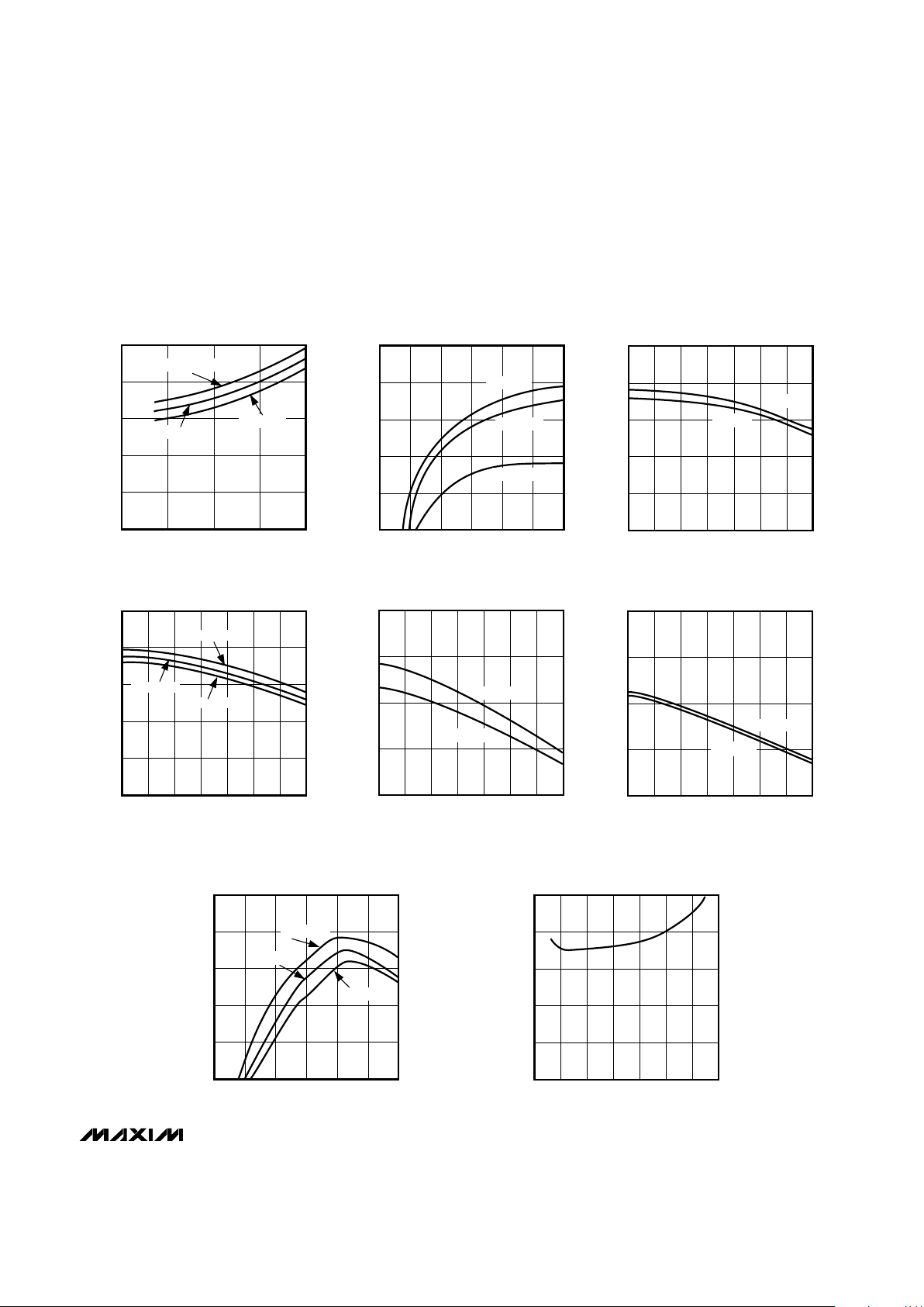
10
8
6
4
2
0
2 3 4 5 6
SUPPLY CURRENT vs. SUPPLY VOLTAGE
MAX2630-1
VCC (V)
I
CC
(mA)
TA = +85°C
TA = -40°C
TA = +25°C
25
20
15
10
5
0
0 5.02.5 10.0 15.0
MAX2632/MAX2633
GAIN vs. SUPPLY CURRENT
MAX2630-2
ICC (mA)
GAIN (dB)
7.5 12.5
f = 0.1GHz
f = 0.9GHz
f = 1.5GHz
20
16
12
8
4
0
0.1 0.3 0.7 1.1 1.3 1.5
GAIN vs. FREQUENCY AND VOLTAGE
MAX2632-3
FREQUENCY (GHz)
GAIN (dB)
0.5 0.9
VCC = 5V
VCC = 3V
-5.0
-7.5
-10.0
-12.5
-15.0
0.1 0.3 0.7 1.1 1.3 1.5
OUTPUT 1dB COMPRESSION
POWER vs. FREQUENCY AND TEMPERATURE
MAX2630-6
FREQUENCY (GHz)
P
-1
(dBm)
0.5 0.9
TA = -40°C
T
A
= +85°C
20
16
12
8
4
0
0.1 0.3 0.7 1.1 1.3 1.5
GAIN vs. FREQUENCY
AND TEMPERATURE
MAX2630-4
FREQUENCY (GHz)
GAIN (dB)
0.5 0.9
TA = -40°C
TA = +85°C
TA = +25°C
-5.0
-7.5
-10.0
-12.5
-15.0
0.1 0.3 0.7 1.1 1.3 1.5
OUTPUT 1dB COMPRESSION
POWER vs. FREQUENCY AND VOLTAGE
MAX2630-5
FREQUENCY (GHz)
P
-1
(dBm)
0.5 0.9
V
CC
= 5V
V
CC
= 3V
0
-4
-8
-12
-16
-20
0 2.5 7.5 12.5 15.0
MAX2632/MAX2633
OUTPUT 1dB COMPRESSION
POWER vs. SUPPLY CURRENT
MAX2630-7
ICC (mA)
P
-1
(dBm)
5.0 10.0
f = 0.1GHz
f = 0.9GHz
f = 1.5GHz
5
4
3
2
1
0
0.1 0.3 0.5 0.9 1.1 1.5
NOISE FIGURE vs. FREQUENCY
MAX2630-8
FREQUENCY (GHz)
NOISE FIGURE (dB)
0.7 1.3

MAX2630–MAX2633
VHF-to-Microwave, +3V,
General-Purpose Amplifiers
4 _______________________________________________________________________________________
______________________________________________________________Pin Description
MAX2630
1
2
3
5
4
—
2
—
IN
GND
3 OUT
V
CC
4
SHDN
6
2
3
4
1
MAX2633
PIN
—
NAME
BIAS51
Amplifier Input. Use a series blocking capacitor with less than
3Ω reactance at your lowest operating frequency.
Ground Connection. For optimum performance, provide a lowinductance connection to the ground plane.
Amplifier Output. Use a series blocking capacitor with less than
3Ω reactance at your lowest operating frequency.
Supply Connection. Bypass directly at the supply pin. The value
of the bypass capacitor is determined by the lowest operating
frequency, and is typically the same as the blocking capacitor
value. Additional bypassing may be necessary for long V
CC
lines.
Shutdown Input. Driving SHDN with a logic low turns off the
amplifier.
FUNCTION
Bias Resistor Connection. Connect a resistor to GND to set the
bias current. See the Supply Current vs. R
BIAS
graph in the
Typical Operating Characteristics
.
—
MAX2632MAX2631
5
2
3
4
1
15
12
9
6
3
0
1 10 100
MAX2632/MAX2633
SUPPLY CURRENT vs. R
BIAS
MAX2630-9
R
BIAS
(kΩ)
I
CC
(mA)
VCC = 5V
VCC = 3V
VCC = 4V
0
0.01
0.03
0.02
0.04
0.05
-40 0-20 20 40 60 80
MAX2631/MAX2633
SHUTDOWN SUPPLY CURRENT
vs. TEMPERATURE
MAX2630 toc11
TEMPERATURE (°C)
SHUTDOWN I
CC
(µA)
VCC = 5.5V
V
CC
= 2.7V
VCC = 3.0V
5:1
4:1
3:1
2:1
1:1
0.1 0.3 0.7 1.1 1.3 1.5
VOLTAGE STANDING-WAVE
RATIO vs. FREQUENCY
MAX2630-10
FREQUENCY (GHz)
VSWR
0.5 0.9
OUT
IN
____________________________Typical Operating Characteristics (continued)
(VCC= +3V, V
SHDN
= VCC(MAX2631/MAX2633), Z0= 50Ω, fIN= 900MHz, R
BIAS
= 10kΩ (MAX2632/MAX2633), TA= +25°C, unless
otherwise noted.)

MAX2630–MAX2633
VHF-to-Microwave, +3V,
General-Purpose Amplifiers
_______________________________________________________________________________________ 5
Table 1a. Typical Scattering Parameters
(VCC= +3V, V
SHDN
= VCC, Z0= 50Ω, R
BIAS
= 10kΩ, TA= +25°C.)
4.30-190.62370.0120.05 -38.7464.3912.9-500.59
3.86-1060.271140.089-21.0121.292.2-1200.222.50
3.81-970.251160.086-21.351.362.6-1150.242.40
3.80-830.241160.077-22.3271.513.6-980.272.20
3.80-630.251170.069-23.3861.634.3-660.312.00
3.76-340.261200.065-23.71441.734.8-260.301.80
3.51-70.261220.066-23.6-1621.915.6-310.241.60
2.90-120.261130.065-23.7-1102.487.9-600.111.40
K
4.07
3.93
3.74
3.61
3.45
3.38
3.27
3.16
3.05
2.87
2.59
S22
(ang)
-29
-49
-71
-94
-118
-109
-96
-82
-68
-53
-25
S22
(mag)
0.57
0.54
0.53
0.51
0.50
0.48
FREQUENCY
(GHz)
0.46
0.44
0.42
0.60
0.40
0.33
S12
(ang)
12
-13
-32
0.50
-51
-70
0.40
-89
-107
-124
0.70
-142
-161
153
0.80
S12
(mag)
0.015
0.016
0.90
0.018
0.019
0.021
1.00
0.022
0.025
0.027
0.10
0.031
0.035
0.20
0.051
S12
(dB)
-36.7
0.30
-35.8
-35.0
-34.4
1.20
-33.6
-33.0
-32.2
-31.3
-30.3
-29.0
-25.8
S21
(ang)
1
-49
-89
-125
-138
-127
-116
-104
-93
-82
-58
S21
(mag)
5.11
5.32
5.32
5.28
5.19
5.05
4.93
4.75
4.49
4.25
3.48
S21
(dB)
14.2
14.5
14.5
14.5
14.3
14.1
13.9
13.5
13.0
12.6
10.8
S11
(ang)
-70
-86
-100
-109
-99
-86
-68
-49
-31
-10
19
S11
(mag)
0.37
0.22
0.17
0.16
0.15
0.14
0.14
0.14
0.13
0.13
0.06

MAX2630–MAX2633
VHF-to-Microwave, +3V,
General-Purpose Amplifiers
6 _______________________________________________________________________________________
0.08
0.12
0.12
0.11
0.11
0.11
0.11
0.12
0.14
0.20
0.58
S11
(mag)
-54
21
-2
-22
-45
-66
-82
-94
-101
-97
-53
S11
(ang)
12.5
14.1
14.5
14.9
15.1
15.2
15.4
15.4
15.4
15.4
13.6
S21
(dB)
4.22
5.09
5.30
5.54
5.68
5.78
5.87
5.91
5.91
5.87
4.80
S21
(mag)
-59
-85
-96
-108
-119
-130
-141
-123
-87
-48
45
S21
(ang)
-25.2
-28.5
-30.0
-31.3
-32.3
-33.1
-33.8
1.20
-34.7
-35.2
-36.1
0.30
-39.2
S12
(dB)
0.055
0.20
0.038
0.032
0.05
0.027
0.024
0.022
1.00
0.020
0.018
0.017
0.90
0.016
0.011
S12
(mag)
0.80
153
-158
-139
0.70
-121
-104
-86
0.40
-68
-50
0.50
-31
-14
36
S12
(ang)
0.34
0.42
0.60
0.43
0.45
0.48
FREQUENCY
(GHz)
0.49
0.51
0.52
0.53
0.55
0.62
S22
(mag)
-18
-49
-65
-79
-94
-108
-119
-95
-72
-49
-22
S22
(ang)
2.01
2.28
2.51
2.73
2.87
3.02
3.14
3.35
3.48
3.75
4.26
K
1.40 0.10 -103 9.3 2.93 -112 -23.1 0.070 114 0.24 -4 2.36
1.60 0.22 -44 6.7 2.16 -163 -23.3 0.068 125 0.24 -7 3.07
1.80 0.29 -20 5.8 1.96 145 -23.7 0.065 124 0.24 -37 3.41
2.00 0.30 -60 5.3 1.85 89 -23.3 0.069 120 0.23 -65 3.41
2.20 0.26 -92 4.9 1.75 29 -22.2 0.078 117 0.21 -83 3.31
2.40 0.24 -110 3.9 1.57 2 -21.7 0.082 116 0.23 -95 3.48
2.50 0.23 -113 3.5 1.50 10 -20.9 0.090 115 0.25 -100 3.35
Table 1b. MAX2633 Typical Scattering Parameters
(VCC= +5V, V
SHDN
= VCC, Z0= 50Ω, R
BIAS
= 10k, TA= +25°C.)
0.35 -76 15.0 5.62 1 -36.90.10 0.014 13 0.57 -29 3.83

MAX2630–MAX2633
VHF-to-Microwave, +3V,
General-Purpose Amplifiers
_______________________________________________________________________________________ 7
_______________Detailed Description
The MAX2630–MAX2633 are broadband amplifiers with
3dB bandwidth greater than 1GHz. Their small size and
internal bias circuitry make them ideal for applications
where board space is limited. The MAX2632/MAX2633
have a user-selectable bias current that allows the user
to set both gain and output power for a particular application, and the MAX2631/MAX2633 incorporate shutdown capability.
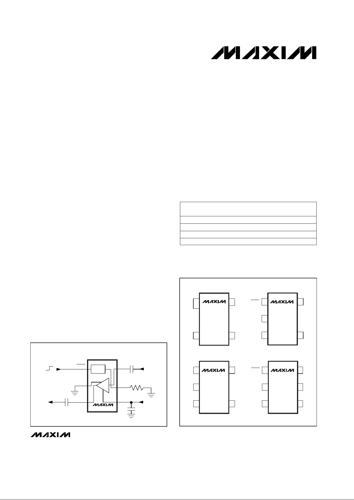
__________Applications Information
External Components
The MAX2630–MAX2633 are easy to use, as shown in the
Typical Operating Circuit
and Figures 1, 2 and 3. Input
and output series capacitors may be necessary to block
DC bias voltages generated by the amplifiers from interacting with adjacent circuitry. These capacitors must be
large enough to contribute negligible reactance in a 50Ω
system at the minimum operating frequency. Use the following equation to calculate their minimum value:
where f (in megahertz) is the minimum operating
frequency.
The VCCpin must be RF bypassed for correct operation. To accomplish this, connect a capacitor between
the VCCpin and ground, as close to the package as is
practical. Use the same equation given above (for DCblocking capacitor values) to calculate the minimum
capacitor value. If the PC board has long VCClines,
additional bypassing may be necessary. This can be
done farther away from the package, if needed.
Proper grounding of the GND pin is essential. If the PC
board uses a topside RF ground, connect it directly to
the GND pin. For a board where the ground plane is not
on the component side, the best technique is to connect the GND pin to it with a plated through-hole close
to the package.
An on-chip buffer at the MAX2631/MAX2633’s SHDN
pin makes bypassing this pin unnecessary except in
very noisy applications. When RF filtering is needed,
use a bypass capacitor similar to the one used on VCC.
Since negligible current flows into this pin, additional
RF filtering may be done with a series resistor.
To set the MAX2632/MAX2633’s supply current,
connect a resistor from the BIAS pin to ground. To
estimate the value of this resistor, refer to the graph
Supply Current vs. R
BIAS
in the
Typical Operating
Characteristics
.
C
BLOCK
=
53,000
f
(pF)
R
BIAS
BIAS
GND
OUT
IN
V
CC
C
BYP
C
BLOCK
V
CC
C
BLOCK
IN
OUT
BIAS
MAX2632
Figure 3. MAX2632 Typical Operating Circuit
OUT
OUT
V
CC
IN
GND
C
BYP
V
CC
C
BLOCK
C
BLOCK
IN
MAX2630
OFF
ON
SHDN
GND
OUT
IN
V
CC
C
BYP
C
BLOCK
V
CC
C
BLOCK
IN
OUT
BIAS
MAX2631
Figure 1. MAX2630 Typical Operating Circuit
Figure 2. MAX2631 Typical Operating Circuit

MAX2630–MAX2633
VHF-to-Microwave, +3V,
General-Purpose Amplifiers
8 _______________________________________________________________________________________
Figure 4. MAX2630 Example PC Board Layout
Figure 5. MAX2631 Example PC Board Layout
Figure 7. MAX2633 Example PC Board LayoutFigure 6. MAX2632 Example PC Board Layout
PC Board Layout Example
Example PC board layouts are given in Figures 4 to 7.
They use FR-4 with a 31mil layer thickness between the
RF lines and the ground plane. The boards satisfy all of
the above recommendations.

MAX2630–MAX2633
VHF-to-Microwave, +3V,
General-Purpose Amplifiers
_______________________________________________________________________________________ 9
P
D
E
F
W
P
2
P
0
D
1
A
0
B
0
K
0
t
W
P
E
F
D
D
1
P
0
P010
P
2
A0
B0
K0
t
8.001
3.988
1.753
3.505
1.499
0.991
3.988
40.005
2.007
3.200
3.099
1.397
0.254
+0.305
-0.102
+0.102
+0.000
+0.254
+0.000
±0.102
±0.102
±0.203
±0.102
±0.051
±0.051
±0.102
±0.102
±0.102
±0.127
NOTE: DIMENSIONS ARE IN MM.
AND FOLLOW EIA481-1 STANDARD.
__________________________________________________Tape-and-Reel Information
___________________Chip Information
TRANSISTOR COUNT: 199

MAX2630–MAX2633
VHF-to-Microwave, +3V,
General-Purpose Amplifiers
10 ______________________________________________________________________________________
________________________________________________________Package Information
SOT1434.EPS

MAX2630–MAX2633
VHF-to-Microwave, +3V,
General-Purpose Amplifiers
______________________________________________________________________________________ 11
___________________________________________Package Information (continued)
SOT5L.EPS

MAX2630–MAX2633
VHF-to-Microwave, +3V,
General-Purpose Amplifiers
6LSOT.EPS
___________________________________________Package Information (continued)
Maxim cannot assume responsibility for use of any circuitry other than circuitry entirely embodied in a Maxim product. No circuit patent licenses are
implied. Maxim reserves the right to change the circuitry and specifications without notice at any time.
12
____________________Maxim Integrated Products, 120 San Gabriel Drive, Sunnyvale, CA 94086 408-737-7600
© 1997 Maxim Integrated Products Printed USA is a registered trademark of Maxim Integrated Products.
 Loading...