For free samples & the latest literature: http://www.maxim-ic.com, or phone 1-800-998-8800.
For small orders, phone 1-800-835-8769.
General Description
The MAX2622/MAX2623/MAX2624 self-contained voltage-controlled oscillators (VCOs) combine an integrated oscillator and output buffer in a miniature 8-pin
µMAX package.
The inductor and varactor elements of the tank circuits
are integrated on-chip, greatly simplifying application of
the part. In addition, the center frequency of oscillation
and frequency span are factory preset to provide a
guaranteed frequency range versus control voltage. An
external tuning voltage controls the oscillation frequency.
The output signals are buffered by an amplifier stage
(easily matched to 50Ω), using only capacitors to pro-
vide higher output power and isolate the devices from
load impedance variations.
The MAX2622/MAX2623/MAX2624 operate from a
+2.7V to +3.3V supply voltage and require only 9mA of
supply current. In shutdown mode, the supply current is
reduced to 0.1µA.
Applications
866MHz to 868MHz European ISM Band (MAX2622)
DECT 1/2 Frequency LO (MAX2623)
902MHz to 928MHz ISM Band, ±10.7MHz IF
(MAX2623)
902MHz to 928MHz ISM Band, 45MHz to 70MHz IF
(MAX2624)
Features
♦ Fully Monolithic
♦ Guaranteed Performance
♦ Wide Choice of Frequencies
855MHz to 881MHz (MAX2622)
885MHz to 950MHz (MAX2623)
947MHz to 998MHz (MAX2624)
♦ +2.7V to +3.3V Single-Supply Operation
♦ Low-Current Shutdown Mode
♦ Smaller than Modules (8-pin µMAX package)
MAX2622/MAX2623/MAX2624
Monolithic Voltage-Controlled Oscillators
________________________________________________________________
Maxim Integrated Products
1
19-1528; Rev 0; 8/99
PART
MAX2622EUA
MAX2623EUA
MAX2624EUA*
-40°C to +85°C
-40°C to +85°C
-40°C to +85°C
TEMP. RANGE PIN-PACKAGE
8 µMAX
8 µMAX
8 µMAX
EVALUATION KIT MANUAL
FOLLOWS DATA SHEET
Ordering Information
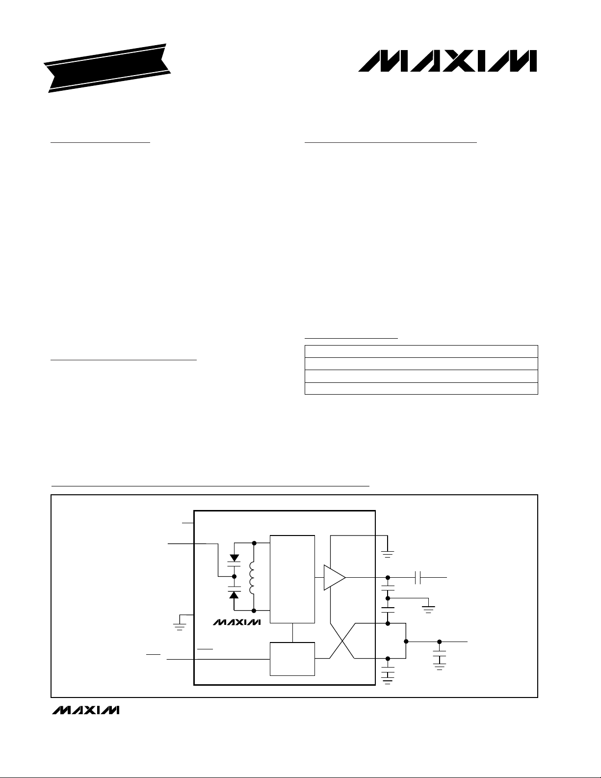
Typical Operating Circuit
Pin Configuration appears at end of data sheet
*
Future product—contact factory for availability.
N.C.
TUNE
SHDN
TUNE
GND
SHDN
OSCILLATOR
CORE
MAX2622
MAX2623
MAX2624
BIAS
GND
OUT
V
V
C
SERIES
C
SHUNT
CC
CC
100pF
100pF
OUT TO MIXER/
SYNTHESIZER
V
CC
0.1µF

MAX2622/MAX2623/MAX2624
Monolithic Voltage-Controlled Oscillators
2 _______________________________________________________________________________________
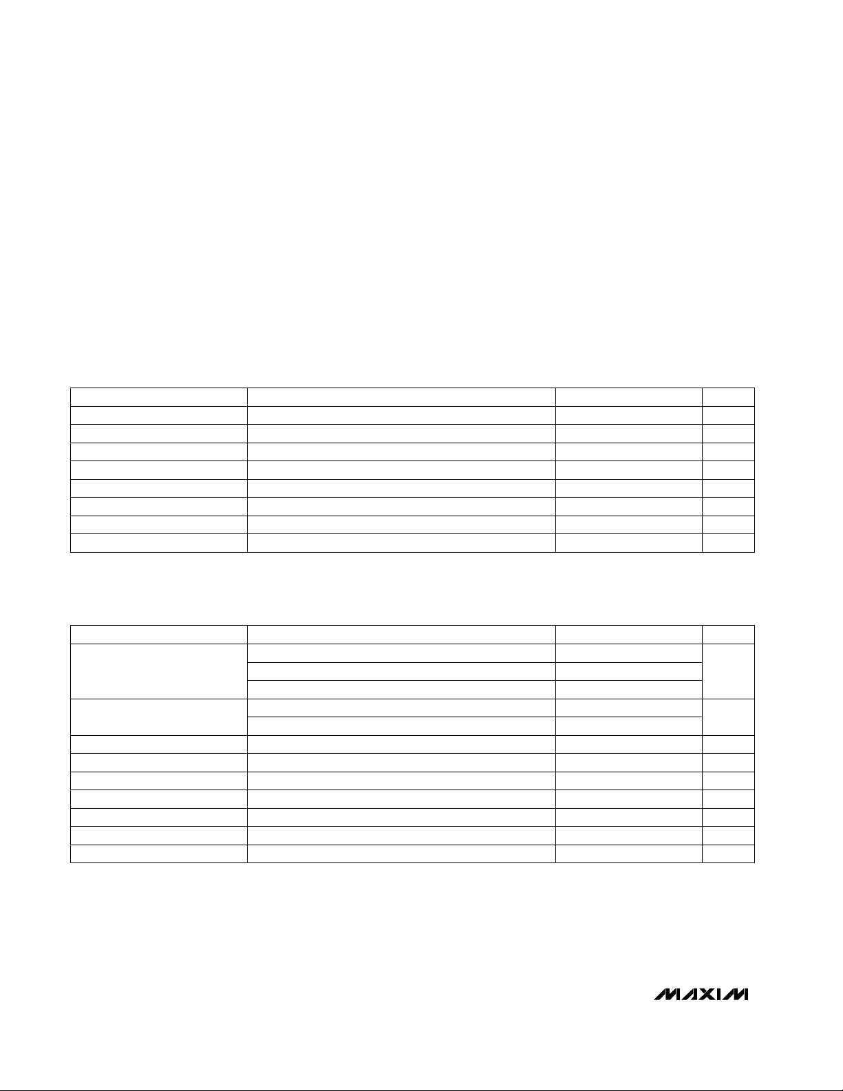
ABSOLUTE MAXIMUM RATINGS
DC ELECTRICAL CHARACTERISTICS
(
Typical Operating Circuit
, VCC= +2.7V to +3.3V, V
TUNE
= 1.4V, V
SHDN
= 2V, OUT = unconnected, TA= -40°C to +85°C, unless
otherwise noted. Typical values are at V
CC
= +3V, TA= +25°C.) (Note 1)
AC ELECTRICAL CHARACTERISTICS
(
Typical Operating Circuit,
VCC= +2.7V to +3.3V, V
TUNE
= 0.4V to 2.4V, V
SHDN
= 2V, TA= +25°C, unless otherwise noted. Typical
values measured at V
CC
= +3V.) (Note 1)
Stresses beyond those listed under “Absolute Maximum Ratings” may cause permanent damage to the device. These are stress ratings only, and functional
operation of the device at these or any other conditions beyond those indicated in the operational sections of the specifications is not implied. Exposure to
absolute maximum rating conditions for extended periods may affect device reliability.
Note 1: Specifications are production tested at T
A
= +25°C. Limits over temperature are guaranteed by design and characterization.
Note 2: Maximum tuning gain is measured at V
TUNE
= 0.4V with a 0.2V step to 0.6V. This represents the worst-case (highest) tuning gain.
Note 3: Measurements taken on MAX262_ EV kit.
Note 4: Return loss is optimized across all frequencies via external shunt/series capacitor matching.
V
CC
to GND..............................................................-0.3V to +6V
TUNE, SHDN to GND .................................-0.3V to (V
CC
+ 0.3V)
OUT to GND ...............................................-0.3V to (V
CC
+ 0.6V)
Continuous Power Dissipation (TA= +70°C)
8-pin µMAX (derate 5.7mW/°C above TA = +70°C)...457mW
Operating Temperature Range ...........................-40°C to +85°C
Junction Temperature......................................................+150°C
Storage Temperature Range .............................-65°C to +150°C
Lead Temperature (soldering, 10sec) .............................+300°C
V
SHDN
≤ 0.6V
0.4V ≤ V
TUNE
2.4V
VCC= 3.3V
VCC= 2.7V
V
SHDN
= 0.6V, VCC= 3.3V
V
SHDN
= 2.0V, VCC= 3.3V
CONDITIONS
µA
0.1 10
Shutdown Supply Current
mA
9 11.5
V
2.7 3.3
Supply Voltage
Supply Current
nA
0.2
TUNE Input Current
V
0.6
SHDN Input Voltage Low
V
2.0
SHDN Input Voltage High
µA
-0.5 0.5
SHDN Input Current Low
µA
-0.5 0.5
SHDN Input Current High
UNITSMIN TYP MAXPARAMETER
f
OFF
= 100kHz
f
OFF
= 1MHz
dBc/Hz
-101
Phase Noise
-119
V
CC
stepped from 2.8V to 3.3V
VSWR = 2:1, all phases
V
TUNE
= 0.4V (Note 3)
CONDITIONS
885 950
kHz/V
200
Supply Pushing
MHz
p-p
0.5
MAX2623, V
TUNE
= 0.4V to 2.4V, TA= -20°C to +75°C
Load Pulling
dBc
-30
Harmonics
dB
-12
Return Loss (Notes 3, 4)
dBm/Hz
-156
Noise Floor
dBm
-8
Output Power
UNITMIN TYP MAXPARAMETER
MAX2622, V
TUNE
= 0.4V to 2.4V, TA= -40°C to +85°C
Oscillator Frequency Range MHz
855 881
V
TUNE
= 0.4V to 2.4V MHz/V
80 110
Tuning Gain (Note 2)
MAX2624, V
TUNE
= 0.4V to 2.4V, TA = -40°C to +85°C
947 998
 Loading...