

Page 1
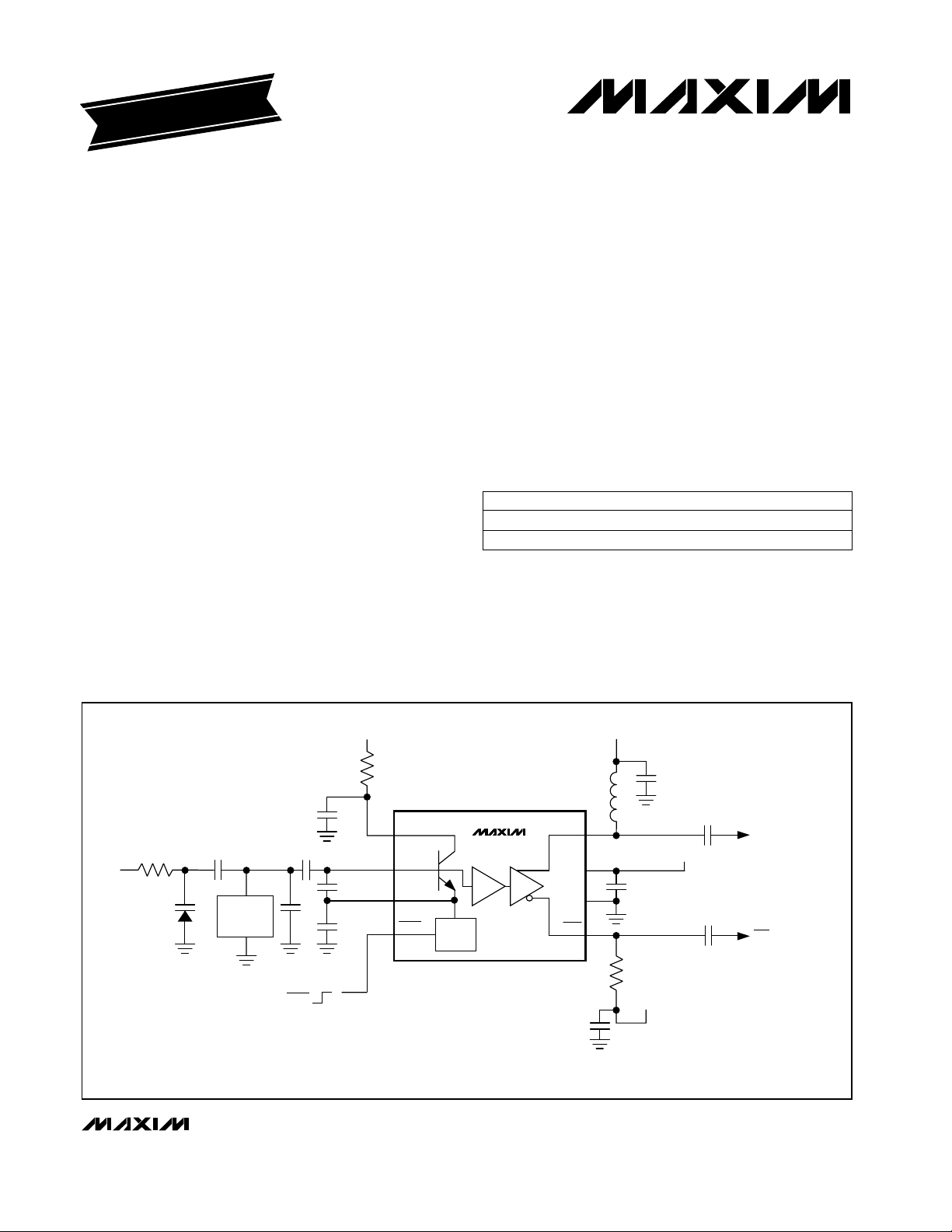
MAX2620
1
V
CC
1
TANK
FDBK
SHDN
2
3
4
8
OUT
V
CC
2
GND
OUT
7
6
5
V
CC
V
CC
V
CC
V
CC
BIAS
SUPPLY
C17
1.5pF
C5
C6
1000pF
1000pF
1000pF
10Ω
CERAMIC
RESONATOR
L1
V
TUNE
900MHz BAND OSCILLATOR
1kΩ
D1
ALPHA
SMV1204-34
1.5pF 1.5pF
51Ω
10nH
C3
2.7pF
C4
1pF
0.1µF
1000pF
OUT TO SYNTHESIZER
OUT TO MIXER
SHDN
MAX2620
10MHz to 1050MHz Integrated
RF Oscillator with Buffered Outputs
________________________________________________________________ Maxim Integrated Products 1
19-1248; Rev 2; 2/02
EVALUATION KIT
AVAILABLE
_________________General Description
The MAX2620 combines a low-noise oscillator with two
output buffers in a low-cost, plastic surface-mount,
ultra-small µMAX package. This device integrates functions typically achieved with discrete components. The
oscillator exhibits low-phase noise when properly
mated with an external varactor-tuned resonant tank
circuit. Two buffered outputs are provided for driving
mixers or prescalers. The buffers provide load isolation
to the oscillator and prevent frequency pulling due to
load-impedance changes. Power consumption is typically just 27mW in operating mode (VCC= 3.0V), and
drops to less than 0.3µW in standby mode. The MAX2620
operates from a single +2.7V to +5.25V supply.
________________________Applications
Analog Cellular Phones
Digital Cellular Phones
900MHz Cordless Phones
900MHz ISM-Band Applications
Land Mobile Radio
Narrowband PCS (NPCS)
____________________________Features
♦ Low-Phase-Noise Oscillator: -110dBc/Hz
(25kHz offset from carrier) Attainable
♦ Operates from Single +2.7V to +5.25V Supply
♦ Low-Cost Silicon Bipolar Design
♦ Two Output Buffers Provide Load Isolation
♦ Insensitive to Supply Variations
♦ Low, 27mW Power Consumption (V
CC
= 3.0V)
♦ Low-Current Shutdown Mode: 0.1µA (typ)
PART
MAX2620EUA -40°C to +85°C
TEMP RANGE PIN-PACKAGE
8 µMAX
_______________Ordering Information
MAX2620E/D -40°C to +85°C Dice*
Pin Configuration appears at end of data sheet.
*Dice are tested at T
A
= +25°C, DC parameters only.
____________________________________________________Typical Operating Circuit
For pricing, delivery, and ordering information, please contact Maxim/Dallas Direct! at
1-888-629-4642, or visit Maxim’s website at www.maxim-ic.com.
Page 2
MAX2620
10MHz to 1050MHz Integrated
RF Oscillator with Buffered Outputs
2 _______________________________________________________________________________________
ABSOLUTE MAXIMUM RATINGS
DC ELECTRICAL CHARACTERISTICS
(VCC1, VCC2 = +2.7V to +5.25V, FDBK = open, TANK = open, OUT and OUT connected to VCCthrough 50Ω, SHDN = 2V,
T
A
= -40°C to +85°C, unless otherwise noted. Typical values measured at VCC1 = VCC2 = 3.0V, TA= +25°C.) (Note 1)
AC ELECTRICAL CHARACTERISTICS
(Test Circuit of Figure 1, VCC= +3.0V, SHDN = VCC, Z
LOAD
= Z
SOURCE
= 50Ω, PIN= -20dBm (50Ω), f
TEST
= 900MHz,
T
A
= +25°C, unless otherwise noted.)
Stresses beyond those listed under “Absolute Maximum Ratings” may cause permanent damage to the device. These are stress ratings only, and functional
operation of the device at these or any other conditions beyond those indicated in the operational sections of the specifications is not implied. Exposure to
absolute maximum rating conditions for extended periods may affect device reliability.
VCC1, VCC2 to GND .................................................-0.3V to +6V
TANK, SHDN to GND .................................-0.3V to (V
CC
+ 0.3V)
OUT, OUT to GND...........................(V
CC
- 0.6V) to (VCC+ 0.3V)
FDBK to GND ..................................(V
CC
- 2.0V) to (VCC+ 0.3V)
Continuous Power Dissipation (T
A
= +70°C)
µMAX (derate 5.7mW/°C above +70°C) .....................457mW
Operating Temperature Range
MAX2620EUA .................................................-40°C to +85°C
Junction Temperature......................................................+150°C
Storage Temperature Range .............................-65°C to +165°C
Lead Temperature (soldering, 10s) .................................+300°C
µA
0.1 2
SHDN = 0.6V
Shutdown Current
mA9.0 12.5
UNITSMIN TYP MAXCONDITIONSPARAMETER
Supply Current
V2.0Shutdown Input Voltage High
V0.6Shutdown Input Voltage Low
µA5.5 20
SHDN = 2.0V
Shutdown Bias Current High
µA0.5
SHDN = 0.6V
Shutdown Bias Current Low
MHz10 1050TA= -40°C to +85°C (Note 2)
UNITSMIN TYP MAXCONDITIONSPARAMETER
Frequency Range
dB50
OUT or OUT to TANK; OUT, OUT driven at P = -20dBm
Reverse Isolation
dB33
OUT to OUT
Output Isolation
Note 2: Guaranteed by design and characterization at 10MHz, 650MHz, 900MHz, and 1050MHz. Over this frequency range, the
magnitude of the negative real impedance measured at TANK is greater than one-tenth the magnitude of the reactive
impedances at TANK. This implies proper oscillator start-up when using an external resonator tank circuit with Q > 10. C3
and C4 must be tuned for operation at the desired frequency.
Note 1: Specifications are production tested and guaranteed at T
A
= +25°C and TA= +85°C. Specifications are guaranteed by
design and characterization at T
A
= -40°C.
Page 3
MAX2620
10MHz to 1050MHz Integrated
RF Oscillator with Buffered Outputs
_______________________________________________________________________________________ 3
TYPICAL OPERATING CIRCUIT PERFORMANCE—900MHz Band CeramicResonator-Based Tank
(Typical Operating Circuit, VCC= +3.0V, V
TUNE
= 1.5V, SHDN = V
CC,
load at OUT = 50Ω, load at OUT = 50Ω, L1 = coaxial ceramic
resonator: Trans-Tech SR8800LPQ1357BY, C6 = 1pF, T
A
= +25°C, unless otherwise noted.)
-110
SSB at ∆f = 25kHz
MHz±13V
TUNE
= 0.5V to 3.0V
UNITSMIN TYP MAXCONDITIONSPARAMETER
Tuning Range
dBc/Hz
-132
SSB at ∆f = 300kHz
Phase Noise
-6 -2At OUT (Note 2)
dBc-29Second-Harmonic Output
MHz/V11Average Tuning Gain
kHz
P-P
163VSWR = 1.75:1, all phasesLoad Pull
kHz/V71VCCstepped from 3V to 4VSupply Pushing
Note 3: Guaranteed by design and characterization.
dBm/Hz-147fO± >10MHzNoise Power
-11 -8
At OUT, per test circuit of Figure 1; TA= -40°C to +85°C
(Note 3)
dBm
-16 -12.5
At OUT (Note 3)
Output Power (Single-Ended)
TYPICAL OPERATING CIRCUIT PERFORMANCE—900MHz Band Inductor-Based Tank
(Typical Operating Circuit, VCC= +3.0V, V
TUNE
= 1.5V, SHDN = V
CC,
load at OUT = 50Ω, load at OUT = 50Ω, L1 = 5nH (Coilcraft
A02T), C6 = 1.5pF, T
A
= +25°C, unless otherwise noted.)
MHz/V13Average Tuning Gain
dBm/Hz-147fO± >10MHzNoise Power
kHz
P-P
340VSWR = 1.75:1, all phase anglesLoad Pull
kHz/V150VCCstepped from 3V to 4VSupply Pushing
-11 -8
At OUT, per test circuit of Figure 1; TA= -40°C to +85°C
(Note 3)
dBm
-16 -12.5
At OUT (Note 3)
Output Power (single-ended)
-107
SSB at ∆f = 25kHz
MHz±15V
TUNE
= 0.5V to 3.0V
UNITSMIN TYP MAXCONDITIONSPARAMETER
Tuning Range
dBc/Hz
-127
SSB at ∆f = 300kHz
Phase Noise
-6 -2At OUT (Note 2)
dBc-29Second-Harmonic Output
Note 3: Guaranteed by design and characterization.
Page 4
MAX2620
10MHz to 1050MHz Integrated
RF Oscillator with Buffered Outputs
4 _______________________________________________________________________________________
__________________________________________Typical Operating Characteristics
(Test Circuit of Figure 1, VCC= +3.0V, SHDN = VCC, Z
LOAD
= Z
SOURCE
= 50Ω, PIN= -20dBm/50Ω, f
TEST
= 900MHz, TA= +25°C,
unless otherwise noted.)
-5
B
C
0
A:
B:
C:
10MHz BAND CIRCUIT
NOT CHARACTERIZED FOR THIS FREQUENCY BAND.
EXPECTED PERFORMANCE SHOWN.
900MHz BAND CIRCUIT
200 400 600 800 1000 1200
OUT OUTPUT POWER vs. FREQUENCY
OVER V
CC
AND TEMPERATURE
-7
MAX2620-01
FREQUENCY (MHz)
POWER (dBm)
-9
-6
-8
TA = +85°C
T
A
= +25°C
T
A
= -40°C
V
CC
= 5.25V
V
CC
= 5.25V
V
CC
= 2.7V
V
CC
= 2.7V
A
-13.0
-13.5
-12.0
-12.5
-11.0
-11.5
0 400200 600 800 1000 1200
OUT OUTPUT POWER vs. FREQUENCY
OVER V
CC
AND TEMPERATURE
MAX2620-02
FREQUENCY (MHz)
POWER (dBm)
V
CC
= 5.25V
V
CC
= 2.7V
TA = +85°C
TA = +25°C
TA = -40°C
FREQUENCY
(MHz)
REAL COMPONENT
(R in Ω)
IMAGINARY COMPONENT
(X in Ω)
250 106 163
350 68 102
450 60 96
550 35 79
1050 6.5 22.7
Table 1. Recommended Load Impedance at OUT or OUT for
Optimum Power Transfer
850
650 17.5 62.3
750 17.2 50.6
10.9 33.1
950 7.3 26.3
Page 5

MAX2620
10MHz to 1050MHz Integrated
RF Oscillator with Buffered Outputs
_______________________________________________________________________________________ 5
_____________________________Typical Operating Characteristics (continued)
(Typical Operating Circuit, VCC= +3.0V, V
TUNE
= 1.5V, SHDN = V
CC,
load at OUT = 50Ω, load at OUT = 50Ω, L1 = coaxial ceramic
resonator: Trans-Tech SR8800LPQ1357BY, C6 = 1pF, T
A
= +25°C, unless otherwise noted.)
REVERSE ISOLATION vs. FREQUENCY
VCC = 2.7V TO 5.25V
0
C3, C4 REMOVED
-10
-20
-30
-40
-50
-60
REVERSE ISOLATION (dB)
-70
-80
-90
50 250 450 650 850 1050
FREQUENCY (MHz)
10MHz BAND CIRCUIT
TYPICAL 1/S11 vs. FREQUENCY
MEASURED AT TEST PORT
15MHz
28 + j79.8
10MHz
63.6 + j121.5
5MHz
262 + j261
MAX2620-03
MAX2620-05
TYPICAL 1/S11 vs. FREQUENCY
10.0
9.5
VCC = 5.25V
9.0
8.5
8.0
SUPPLY CURRENT (mA)
7.5
900MHz BAND CIRCUIT*
MEASURED AT TEST PORT
1050MHz
21 + j78
900MHz
36 + j90
800MHz
49 + j105
650MHz
84 + j142
*SEE FIGURE 1
SUPPLY CURRENT
vs. TEMPERATURE
VCC = 2.7V
MAX2620-04
MAX2620-06
C3 = C4 = 270pF
L3 = 10µH
C2 = C10 = C13 = 0.01µF
7.0
-20 0 20 40 60 80 100
-40
TEMPERATURE (°C)
Page 6

MAX2620
10MHz to 1050MHz Integrated
RF Oscillator with Buffered Outputs
6 _______________________________________________________________________________________
_______________________________________________________________Pin Description
NAME FUNCTIONPIN
3 FDBK
Oscillator Feedback Circuit Connection. Connecting capacitors of the appropriate value between FDBK and
TANK and between FDBK and GND tunes the oscillator’s reflection gain (negative resistance) to peak at the
desired oscillation frequency. Refer to the Applications Information section.
2 TANK Oscillator Tank Circuit Connection. Refer to the Applications Information section.
1 VCC1
Oscillator DC Supply Voltage. Decouple VCC1 with 1000pF capacitor to ground. Use a capacitor with low
series inductance (size 0805 or smaller). Further power-supply decoupling can be achieved by adding a
10Ω resistor in series from VCC1 to the supply. Proper power-supply decoupling is critical to the low noise
and spurious performance of any oscillator.
8 OUT
Open-Collector Output Buffer. Requires external pull-up to the voltage supply. Pull-up can be resistor,
choke, or inductor (which is part of a matching network). The matching-circuit approach provides the highest-power output and greatest efficiency. Refer to Table 1 and the Applications Information section. OUT
can be used with OUT in a differential output configuration.
7 VCC2
Output Buffer DC Supply Voltage. Decouple VCC2 with a 1000pF capacitor to ground. Use a capacitor with
low series inductance (size 0805 or smaller).
6 GND Ground Connection. Provide a low-inductance connection to the circuit ground plane.
5
OUT
Open-Collector Output Buffer (complement). Requires external pull-up to the voltage supply. Pull-up can be
resistor, choke, or inductor (which is part of a matching network). The matching-circuit approach provides
the highest-power output and greatest efficiency. Refer to Table 1 and the Applications Information section.
OUT can be used with OUT in a differential output configuration.
4
SHDN
Logic-Controlled Input. A low level turns off the entire circuitry such that the IC will draw only leakage current
at its supply pins. This is a high-impedance input.
_____________________________Typical Operating Characteristics (continued)
(Typical Operating Circuit, VCC= +3.0V, V
TUNE
= 1.5V, SHDN = V
CC,
load at OUT = 50Ω, load at OUT = 50Ω, L1 = coaxial ceramic
resonator: Trans-Tech SR8800LPQ1357BY, C6 = 1pF, T
A
= +25°C, unless otherwise noted.)
-114
-112
-110
-108
-106
-104
-40 -20 0 20 40 60 80
PHASE NOISE vs. TEMPERATURE
MAX2620-07
TEMPERATURE (°C)
SSB PHASE NOISE (dBc/Hz)
SSB @ ∆f = 25kHz
L1 = 5nH INDUCTOR
C6 = 1.5pF
L1 = COAXIAL CERAMIC RESONATOR
(TRANS-TECH SR8800LPQ1357BY)
C6 = 1pF
-100
-90
-80
-70
-60
-50
-40
-30
-20
-10
0
0 1.3 2.6 3.9 5.2 6.5
OUTPUT SPECTRUM
FUNDAMENTAL NORMALIZED TO 0dB
MAX2620-08
FREQUENCY (GHz)
RELATIVE OUTPUT LEVEL (dBc)
-150
-140
-130
-120
-110
-100
-90
-80
-70
-60
-50
-40
0.1 10 1000100
SINGLE SIDEBAND PHASE NOISE
MAX2620-09
OFFSET FREQUENCY (kHz)
SSB PHASE NOISE (dBc/Hz)
1
L1 = 5nH INDUCTOR
C6 = 1.5pF
L1 = COAXIAL
CERAMIC RESONATOR
(TRANS-TECH
SR8800LPQ1357BY)
C6 = 1pF
Page 7

MAX2620
10MHz to 1050MHz Integrated
RF Oscillator with Buffered Outputs
_______________________________________________________________________________________ 7
_______________Detailed Description
Oscillator
The oscillator is a common-collector, negativeresistance type that uses the IC’s internal parasitic elements to create a negative resistance at the baseemitter port. The transistor oscillator has been optimized for low-noise operation. Base and emitter leads
are provided as external connections for a feedback
capacitor and resonator. A resonant circuit, tuned to
the appropriate frequency and connected to the base
lead, will cause oscillation. Varactor diodes may be
used in the resonant circuit to create a voltage-controlled oscillator (VCO). The oscillator is internally
biased to an optimal operating point, and the base and
emitter leads need to be capacitively coupled due to
the bias voltages present.
Output Buffers
The output buffers (OUT and OUT) are an opencollector, differential-pair configuration and provide
load isolation to the oscillator. The outputs can be used
differentially to drive an integrated circuit mixer.
Alternatively, isolation is provided between the buffer
outputs when one output drives a mixer (either upconversion or downconversion) and the other output drives
a prescaler. The isolation in this configuration prevents
prescaler noise from corrupting the oscillator signal’s
spectral purity.
A logic-controlled SHDN pin turns off all bias to the IC
when pulled low.
__________Applications Information
Design Principles
At the frequency of interest, the MAX2620 portion of
Figure 2 shows the one-port circuit model for the TANK
pin (test port in Figure 1).
For the circuit to oscillate at a desired frequency, the resonant tank circuit connected to TANK must present an
impedance that is a complement to the network
(Figure 2). This resonant tank circuit must have a positive
real component that is a maximum of one-half the magnitude of the negative real part of the oscillator device, as
well as a reactive component that is opposite in sign to
the reactive component of the oscillator device.
Figure 2. Simplified Oscillator Circuit Model
MAX2620
1
2
V
CC
1
TANK
FDBK
SHDN
3
4
8
OUT
V
CC
2
OUT
GND
7
6
5
V
CC
V
CC
V
CC
VCC
V
CC
TEST PORT
BIAS
SUPPLY
C13*
1000pF
C2*
1000pF
ON
OFF
1000pF
1000pF
1000pF
10Ω
10Ω
L3*
220nH
51Ω
C3*
2.7pF
C4*
1pF
1000pF
1000pF
C10*
1000pF
Z
O
= 50Ω
*AT 10MHz, CHANGE TO:
C3 = C4 = 270pF
L3 = 10µH
C2 = C10 = C13 = 0.01µF
Z
O
= 50Ω
OUT
OUT
Figure 1. 900MHz Test Circuit
TANK
-jX
T
OSCILLATOR
DEVICE
jX
TIMES R
L
LESS THAN 1/2
L
RESONANT
TANK
-R
n
Page 8

MAX2620
10MHz to 1050MHz Integrated
RF Oscillator with Buffered Outputs
8 _______________________________________________________________________________________
Keeping the resonant tank circuit’s real component less
than one-half the magnitude of the negative real component ensures that oscillations will start. After start-up,
the oscillator’s negative resistance decreases, primarily
due to gain compression, and reaches equilibrium with
the real component (the circuit losses) in the resonant
tank circuit. Making the resonant tank circuit reactance
tunable (e.g., through use of a varactor diode) allows
for tuneability of the oscillation frequency, as long as
the oscillator exhibits negative resistance over the
desired tuning range. See Figures 3 and 4.
The negative resistance of the MAX2620 TANK pin can
be optimized at the desired oscillator frequency by
proper selection of feedback capacitors C3 and C4.
For example, the one-port characteristics of the device
are given as a plot of 1/S11 in the Typical Operating
Characteristics. 1/S11 is used because it maps inside
the unit circle Smith chart when the device exhibits
negative resistance (reflection gain).
Figure 3. 10MHz VCO LC Resonator
V
TUNE
C5
150pF
1kΩ
C17
33pF
C6
33pH
D1
L1
2.2µH
C3
270pF
C4
270pF
V
CC
10Ω
1000pF
1
VCC1
MAX2620
2
TANK
3
FDBK
4
SHDN
OUT
V
GND
OUT
CC
1000pF
2
10µH
8
7
6
5
V
CC
27pF
0.01µF
V
CC
1000pF
0.01µF
OUT TO
MIXER
OUT TO
SYNTHESIZER
SHDN
D1 = SMV1200-155 DUAL VARACTOR
51Ω
1000pF
V
CC
Page 9

MAX2620
10MHz to 1050MHz Integrated
RF Oscillator with Buffered Outputs
_______________________________________________________________________________________ 9
Sample Calculation
According to the electrical model shown in Figure 5, the
resonance frequency can be calculated as:
[Equation 1]
R
n
, the negative real impedance, is set by C3 and C4
and is approximately:
[Equation 2]
where gm= 18mS.
Using the circuit model of Figure 5, the following example describes the design of an oscillator centered at
900MHz.
Choose: L1 = 5nH ±10%
Q = 140
Calculate: R
p
= Q ×2π×f ×L1
Using Equation 1, solve for varactor capacitance (CD1).
CD1is the capacitance of the varactor when the voltage applied to the varactor is approximately at halfsupply (the center of the varactor’s capacitance range).
Assume the following values:
C
STRAY
= 2.7pF, C17 = 1.5pF, C6 = 1.5pF, C5 = 1.5pF,
C03= 2.4pF, C04= 2.4pF, C3 = 2.7pF, and C4 = 1pF
The value of C
STRAY
is based on approximate performance of the MAX2620 EV kit. Values of C3 and C4 are
chosen to minimize Rn(Equation 2) while not loading
the resonant circuit with excessive capacitance. C
03
and C04are parasitic capacitors.
The varactor’s capacitance range should allow for the
desired tuning range. Across the tuning frequency
range, ensure that Rs< 1/2 Rn.
The MAX2620’s oscillator is optimized for low-phasenoise operation. Achieving lowest phase-noise characteristics requires the use of high-Q (quality factor)
components such as ceramic transmission-line type
Figure 4. 10MHz Crystal Oscillator
V
CC
10Ω
0.01µF
1
VCC1
30pF
120pF
120pF
SHDN
X = STATEK AT-3004 10MHz
FUNDAMENTAL MODE CRYSTAL SURFACE MOUNT
= 20pF
C
LOAD
2
TANK
MAX2620
3
FDBK
4
SHDN
OUT
V
GND
OUT
V
CC
0.01µF
10µH
8
7
2
CC
6
5
51Ω
27pF
0.01µF
V
CC
0.01µF
0.01µF
0.01µF
V
CC
OUT
OUT
f
=
O
2 L1 C +
π
where C
=
n
STRAY
C + C C + C
()()
303404
C + C + C + C
303404
1
C x C
17 D1
C + C
17 D1
C
++
6
C x C
5n
C + C
5n
Rg
=
nm
2
1
ππ
fC C fC C
()
303 404
+
2
()
1
+
Page 10

MAX2620
10MHz to 1050MHz Integrated
RF Oscillator with Buffered Outputs
10 ______________________________________________________________________________________
resonators or high-Q inductors. Also, keep C5 and C17
(see the Typical Operating Circuit) as small a value as
possible while still maintaining desired frequency and
tuning range to maximize loaded Q.
There are many good references on the topic of oscillator design. An excellent reference is “The Oscillator
as a Reflection Amplifier, an Intuitive Approach to
Oscillator Design,” by John W. Boyles, Microwave
Journal, June 1986, pp. 83–98.
Output Matching Configuration
Both of the MAX2620’s outputs (OUT and OUT) are
open collectors. They need to be pulled up to the supply by external components. An easy approach to this
pull-up is a resistor. A 50Ω resistor value would inherently match the output to a 50Ω system. The Typical
Operating Circuit shows OUT configured this way.
Alternatively, a choke pullup (Figure 1), yields greater
output power (approximately -8dBm at 900MHz).
When maximum power is required, use an inductor as
the supply pull-up, and match the inductor’s output
impedance to the desired system impedance. Table 1
in the Typical Operating Characteristics shows recommended load impedance presented to OUT and OUT
for maximum power transfer. Using this data and standard matching-network synthesis techniques, a matching network can be constructed that will optimize power
output into most load impedances. The value of the
inductor used for pullup should be used in the synthesis of the matching network.
__________________Pin Configuration
Figure 5. Electrical Model of MAX2620 Circuit
+ jX
R
S
C
PC BOARD
PARASITICS
STRAY
C17
C
D1
VARACTOR+
COUPLING
L1
R
p
INDUCTOR
OR
CERAMIC
RESONATOR
S
C5
C6
TEST PORT
MEASUREMENT
(FIGURE 1)
MAX2620
C
C3
C4
03
2.4pF
C
04
2.4pF
R
n
RESONANT TANK MODEL
MAX2620 PACKAGE MODEL
TOP VIEW
1
V
1
CC
2
TANK
FDBK
SHDN
3
4
MAX2620
µMAX
8
OUT
2
V
7
CC
GND
6
5
OUT
Page 11

MAX2620
10MHz to 1050MHz Integrated
RF Oscillator with Buffered Outputs
Maxim cannot assume responsibility for use of any circuitry other than circuitry entirely embodied in a Maxim product. No circuit patent licenses are
implied. Maxim reserves the right to change the circuitry and specifications without notice at any time.
Maxim Integrated Products, 120 San Gabriel Drive, Sunnyvale, CA 94086 408-737-7600 ____________________ 11
© 2002 Maxim Integrated Products Printed USA is a registered trademark of Maxim Integrated Products.
Package Information
(The package drawing(s) in this data sheet may not reflect the most current specifications. For the latest package outline information,
go to www.maxim-ic.com/packages.)
0.6±0.1
0.6±0.1
8
b
E H
A1
A
ÿ 0.50±0.1
1
D
TOP VIEW
A2
e
FRONT VIEW
4X S
BOTTOM VIEW
c
L
SIDE VIEW
8
1
DIM
A
A1
A2
b
c
D
e
E
H
L
α
S
INCHES
MIN
-
0.002
0.030
0.010
0.005
0.116
0.0256 BSC
0.116
0.188
0.016
0∞
0.0207 BSC
MAX
0.043
0.006
0.037
0.014
0.007
0.120
0.120
0.198
0.026
6∞
MILLIMETERS
MIN
0.05 0.15
0.25 0.36
0.13 0.18
2.95 3.05
2.95 3.05
4.78
0.41
MAX
- 1.10
0.950.75
0.65 BSC
5.03
0.66
6∞0∞
0.5250 BSC
α
8LUMAXD.EPS
PROPRIETARY INFORMATION
TITLE:
PACKAGE OUTLINE, 8L uMAX/uSOP
REV.DOCUMENT CONTROL NO.APPROVAL
21-0036
1
J
1
 Loading...