

19-1094; Rev 0; 6/96
EVALUATION KIT
AVAILABLE
DC-to-Microwave, Low-Noise Amplifier
_______________General Description
The MAX2611 is a low-voltage, low-noise amplifier for
use from DC to microwave frequencies. Operating from
a single +5V supply, it has a 3dB bandwidth of
1100MHz. The MAX2611’s low noise figure and high
drive capability make it ideal for a variety of transmit,
receive, and buffer applications.
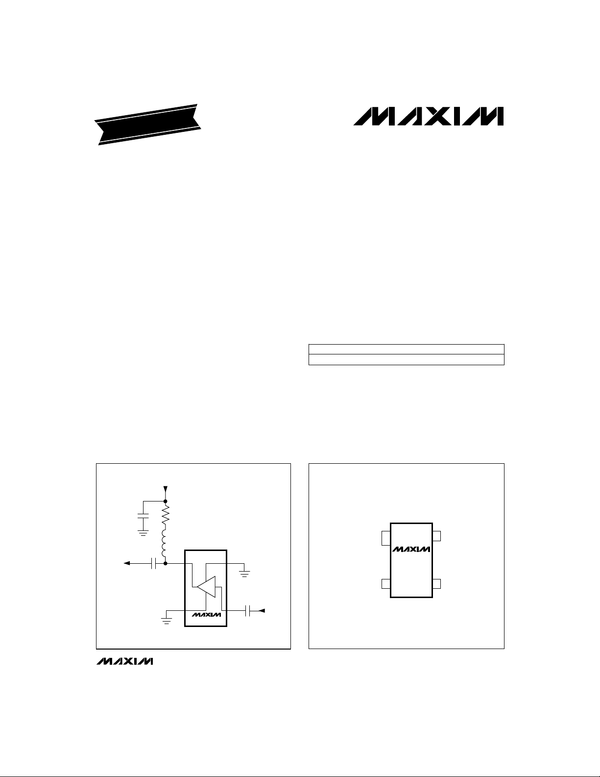
In a typical application, the only external components
needed are input and output blocking capacitors and
a VCCseries resistor. To improve gain and output
power, an RF choke can be added in series to the bias
resistor.
The MAX2611 comes in a 4-pin SOT143 package,
requiring minimal board space.
________________________Applications
Satellite Receivers
TV Tuners
Wireless Local Loops
ISM Radios
Global Positioning Systems
Wireless Local-Area Networks
Land Mobile Radios
Set-Top Boxes
__________Typical Operating Circuit
____________________________Features
♦ Single +5V Supply Operation
♦ 3dB Bandwidth: DC to 1100MHz
♦ High Gain: 18dB at 500MHz
♦ Low Noise Figure: 3.5dB at 500MHz
♦ High Drive Capability: +3dBm at 16mA I
D
♦ Ultra-Small SOT143 Package
________________Ordering Information
PART
MAX2611EUS -40°C to +85°C
TEMP. RANGE PIN-PACKAGE
4 SOT143
__________________Pin Configuration
MAX2611
V
C
BYP
(OPTIONAL)
OUT
CC
R
BIAS
L
CHOKE
(OPTIONAL)
OUT
C
BLOCK
GND
MAX2611
________________________________________________________________
GND
IN
C
IN
BLOCK
TOP VIEW
OUT
3
MAX2611
GND
21IN
SOT143
Maxim Integrated Products
GND
4
1
For free samples & the latest literature: http://www.maxim-ic.com, or phone 1-800-998-8800
DC-to-Microwave, Low-Noise Amplifier
ABSOLUTE MAXIMUM RATINGS
I
.........................................................................................40mA
D
Input Power ....................................................................+13dBm
Continuous Power Dissipation (T
SOT143-4 (derate 4mW/°C above +70°C)..................320mW
Stresses beyond those listed under “Absolute Maximum Ratings” may cause permanent damage to the device. These are stress ratings only, and functional
operation of the device at these or any other conditions beyond those indicated in the operational sections of the specifications is not implied. Exposure to
absolute maximum rating conditions for extended periods may affect device reliability.
= +70°C)
A
Operating Temperature Range ...........................-40°C to +85°C
Junction Temperature......................................................+150°C
Storage Temperature Range.............................-65°C to +150°C
Lead Temperature (soldering, 10sec).............................+300°C
MAX2611
ELECTRICAL CHARACTERISTICS
(ID= 16mA, Z0= 50Ω, fIN= 500MHz, TA= +25°C, unless otherwise noted.)
CONDITIONS
(Note 1)
Power Gain
Input Voltage Standing-Wave
Maximum Ratio
Output Voltage Standing-Wave
Maximum Ratio
Device Voltage V
Device Voltage
Temperature Coefficient
fIN= 100MHz
fIN= 500MHz 17.3 18.3
= 100MHz to 500MHz
f
IN
fIN= 100MHz to 1500MHz
fIN= 100MHz to 1500MHz
TA= T
MIN
to T
(Note 2) 3.25 3.8 4.26
MAX
19.0
1.9:1
1.6:1
3.5 3.8 4.0
UNITSMIN TYP MAXPARAMETER
°C-40 85Operating Temperature Range
dB
dB±0.3Gain Flatness
MHz11003dB Bandwidth
dBm2.9Output 1dB Compression Point
dB3.5Noise Figure
dBm13Output IP3
ps210Group Delay
mV/°C-6.1
Note 1: Parts are designed to operate over specified temperature range. Specifications are production tested and guaranteed
at +25°C.
Note 2: Guaranteed by design, not tested.
2 _______________________________________________________________________________________

DC-to-Microwave, Low-Noise Amplifier
__________________________________________Typical Operating Characteristics
(ID = 16mA, Z0= 50Ω, fIN= 500MHz, TA= +25°C, unless otherwise noted.)
25
GAIN vs. FREQUENCY
20
15
GAIN (dB)
10
5
0
0.05 0.10 0.30 0.50 1.00
FREQUENCY (GHz)
NOISE FIGURE (dB)
TA = -40°C
TA = +85°C
NOISE FIGURE vs. FREQUENCY
7
6
5
4
3
3.00 6.00
TA = +85°C
TA = +25°C
TA = -40°C
MAX2611-01
VOLTAGE STANDING-WAVE RATIO
vs. FREQUENCY
5:1
4:1
3:1
VSWR
2:1
1:1
0.05 0.10 0.30 0.50 1.00
FREQUENCY (GHz)
MAX2611-04
IN
OUT
3.00 6.00
25
20
15
GAIN (dB)
10
5
MAX2611-02
(dBm)
-1
P
GAIN vs. CURRENT
0.16GHz
OUTPUT 1dB COMPRESSION
POINT vs. FREQUENCY
5
4
3
2
1
0
TA = +85°C
TA = -40°C
0.1 0.2 0.3 0.4
1.0GHz
2.0GHz
FREQUENCY (GHz)
0.5GHz
TA = +25°C
0.5
MAX2611-05
1.0 2.0
MAX2611
MAX2611-03
2
0.2
0.1
0.3 0.4 0.5
FREQUENCY (GHz)
1.0 2.0
0
10 15 20 25
ID(mA)
30
35
_______________________________________________________________________________________
3

DC-to-Microwave, Low-Noise Amplifier
______________________________________________________________Pin Description
PIN
1
2, 4 GND
MAX2611
3
NAME FUNCTION
IN
OUT
Amplifier Input. Use a series blocking capacitor with less than 3Ω reactance at your lowest operating
frequency.
Ground Connection. For optimum performance, provide a low-inductance connection to the ground
plane.
Amplifier Output. Use a series blocking capacitor with less than 3Ω reactance at your lowest operating frequency. Bias with an external resistor and an optional RF choke.
Table 1. Typical Scattering Parameters
(ID= 16mA, Z0= 50Ω, TA= +25°C)
FREQUENCY
(GHz)
0.1
0.2
0.3
0.4
0.5
0.6
0.8
1.0
1.5
2.0
2.5
3.0
3.5 0.24 -64 3.0 1.41 13 -21.4 0.086 30 0.19 47 3.83
4.0
S11
(mag)
0.12
0.11
0.13
0.14
0.15
0.15
0.13
0.12
0.32
0.31
0.32
0.20
0.31 -68 -0.7 0.92 17 -23.0 0.070 35 0.24 82 6.66
S11
(ang)
-11
-44
-58
-78
-89
77
50
16
-60
-72
-76
-70
S21
(dB)
19.0
18.8
18.6
18.5
18.3
18.1
17.4
16.6
14.1
10.3
7.9
5.9
S21
(mag)
8.90
8.73
8.53
8.43
8.26
7.99
7.45
6.79
5.07
3.27
2.48
1.98
S21
(ang)
173
166
158
151
144
137
123
109
79
59
47
32
S12
(dB)
-22.6
-21.9
-21.6
-21.6
-21.6
-21.6
-21.6
-20.9
-21.8
-22.2
-22.6
-22.3
S12
(mag)
0.074
0.081
0.083
0.083
0.083
0.083
0.083
0.090
0.081
0.078
0.074
0.077
S12
(ang)
2
4
5
6
7
9
10
10
11
18
25
37
S22
(mag)
0.05
0.03
0.04
0.06
0.08
0.09
0.10
0.10
0.21
0.22
0.26
0.24
S22
(ang)
53
12
45
32
34
26
23
35
-86
-72
-53
-29
K
1.08
1.06
1.05
1.06
1.06
1.07
1.10
1.11
1.29
1.87
2.44
3.10
4 _______________________________________________________________________________________

DC-to-Microwave, Low-Noise Amplifier
_______________Detailed Description
The MAX2611 is a broadband amplifier with flat gain
and 50Ω input and output ports. Its small size and simple bias circuitry make it ideal for applications where
board space is limited.
__________Applications Information
As shown in the
MAX2611 is easy to use. Input and output series
capacitors may be necessary to block DC bias voltages (generated by the MAX2611) from interacting with
adjacent circuitry. These capacitors must be large
enough to contribute negligible reactance in a 50Ω
system at the minimum operating frequency. Use the
following equation to calculate their minimum value:
C
BLOCK
where f (in MHz) is the minimum operating frequency.
Bias current is supplied to the MAX2611 through an
external resistor and optional RF choke connected
between V
from VCCto GND may be necessary to isolate the V
line from other circuitry. The resistor value determines
the bias current from the following equation:
and the OUT pin. A bypass capacitor
CC
External Components
Typical Operating Circuit
53,000
=
V
CC
I
=
D
R
f
- V
BIAS
(pF)
D
, the
CC
Proper grounding of the GND pins is essential. If the
Grounding
PC board uses a topside RF ground, the GND pins
should be connected directly to it. For a board where
the ground plane is not on the component side, the
best technique is to connect the GND pins to it through
multiple plated through-holes.
PC Board Layout Example
An example PC board layout is given in Figure 1. It
uses FR-4 with 31mil layer thickness between the RF
lines and the ground plane. This board satisfies all the
above requirements.
MAX2611
where V
An optional RF choke can be added to improve the
MAX2611’s gain and output power. The choke should
be large enough to reduce the loading effect that the
bias resistor has on the amplifier output. This is a function of R
impedance.
is the device voltage, nominally 3.8V.
D
, frequency of operation, and output
BIAS
_______________________________________________________________________________________ 5
EXPANDED VIEW
Figure 1. Example PC Board Layout

DC-to-Microwave, Low-Noise Amplifier
__________________________________________________Tape-and-Reel Information
4.0 ±0.1
1.5 +0.1/-0.0 DIAMETER
MAX2611
1.0 ±0.1
2.0 ±0.05
A
1.75 ±0.1
3.5 ±0.05
8.0 ±0.3
2.2 ±0.1
MARKING
0.5 RADIUS
TYPICAL
0.30 ±0.05
0.8 ±0.05
0.30R MAX.
A0
A
NOTE: DIMENSIONS ARE IN MM.
AND FOLLOW EIA481-1 STANDARD.
Bo
4.0 ±0.1
Ao = 3.1mm ±0.1
Bo = 2.7mm ±0.1
Ko
Ko = 1.2mm ±0.1
†
ICs MAY ALSO BE MARKED WITH FULL PART NAME: 2611
1.0 MINIMUM
INFORMATION
X X X X
DF = MAX2611
LOT SPECIFIC
CODE
________________________________________________________Package Information
D
0°-8°
A
A1
e1
B
I
DIM
MIN
A
0.031
A1
0.001
B
C
0.014
B1
0.030
C
0.0034
D
0.105
E
0.047
e
0.070
e1
0.071
H
0.082
I
0.004
MAX
0.047
0.005
0.022
0.038
0.006
0.120
0.055
0.080
0.079
0.098
0.012
MILLIMETERSINCHES
MIN
0.787
0.025
0.356
0.762
0.086
2.667
1.194
1.778
1.803
2.083
0.102
†
21-0052A
MAX
1.194
0.127
0.559
0.965
0.152
3.048
1.397
2.032
2.007
2.489
0.305
E
H
4-PIN SOT143
SMALL-OUTLINE
TRANSISTOR PACKAGE
B1
Maxim cannot assume responsibility for use of any circuitry other than circuitry entirely embodied in a Maxim product. No circuit patent licenses are
implied. Maxim reserves the right to change the circuitry and specifications without notice at any time.
6
___________________Maxim Integrated Products, 120 San Gabriel Drive, Sunnyvale, CA 94086 (408) 737-7600
© 1996 Maxim Integrated Products Printed USA is a registered trademark of Maxim Integrated Products.
e
 Loading...