

Page 1
General Description
The MAX2605–MAX2609 are compact, high-performance
intermediate-frequency (IF) voltage-controlled oscillators
(VCOs) designed specifically for demanding portable
wireless communication systems. They combine monolithic construction with low-noise, low-power operation in a
tiny 6-pin SOT23 package.
These low-noise VCOs feature an on-chip varactor and
feedback capacitors that eliminate the need for external
tuning elements, making the MAX2605–MAX2609 ideal
for portable systems. Only an external inductor is
required to set the oscillation frequency. In addition, an
integrated differential output buffer is provided for driving a mixer or prescaler. The buffer output is capable
of supplying up to -8dBm (differential) with a simple
power match. It also provides isolation from load
impedance variations.
The MAX2605–MAX2609 operate from a single +2.7V to
+5.5V supply and offer low current consumption. These IF
oscillators can cover the 45MHz to 650MHz frequency
range.
Applications
Cellular and PCS Mobile Phones
2.4GHz ISM Band
902MHz to 928MHz ISM Band
Land Mobile Radio
GPS Receivers
General-Purpose IF Oscillators
Features
♦ Small Size
♦ Integrated Varactor for Tuning
♦ Low Phase Noise
♦ Wide Application Frequency Range
♦ Differential or Single-Ended Outputs
♦ Single +2.7V to +5.5V Supply
♦ Ultra-Small SOT23-6 Package
♦ On-Chip Temperature-Stable Bias
♦ Low-Current Operation
MAX2605–MAX2609
45MHz to 650MHz, Integrated IF
VCOs with Differential Output
________________________________________________________________ Maxim Integrated Products 1
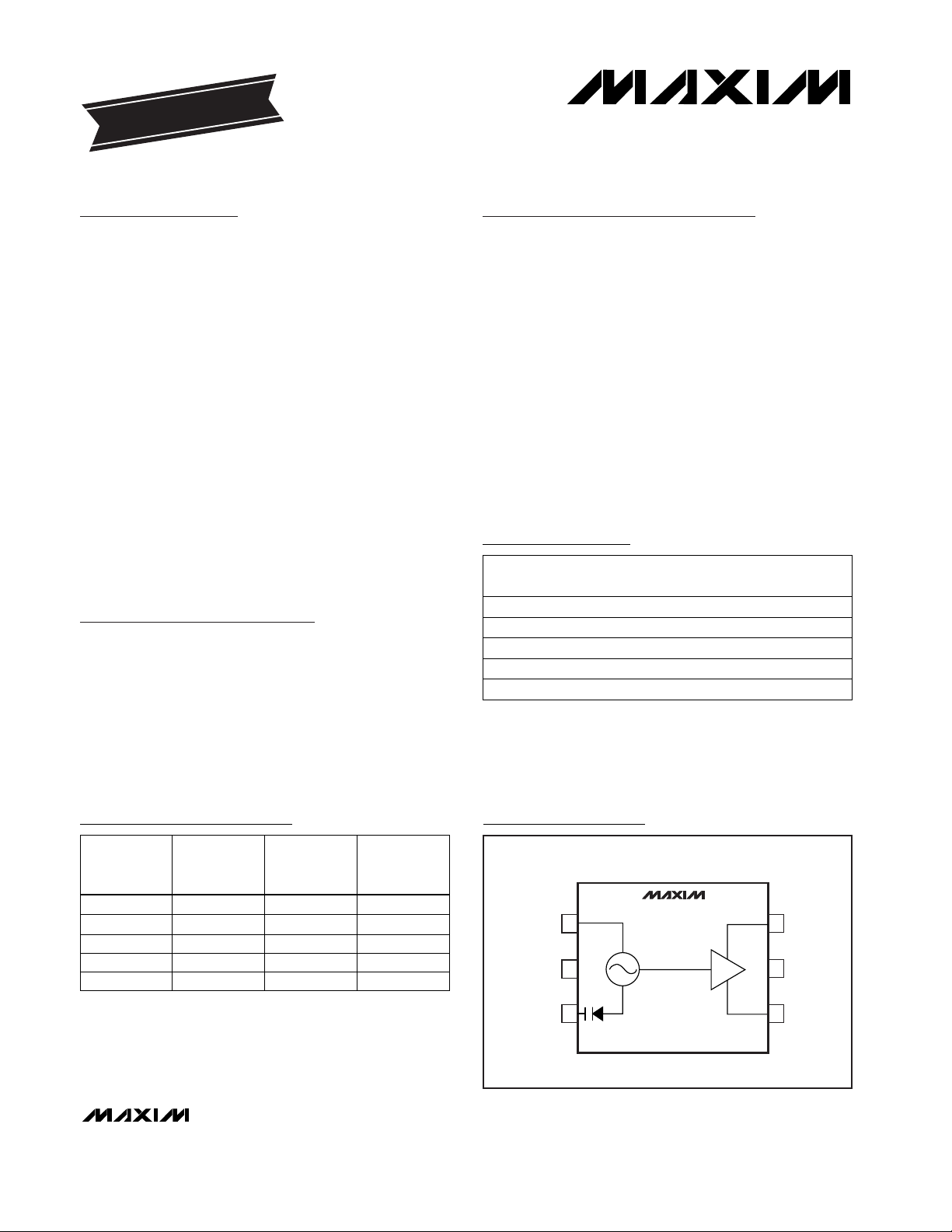
GND
OUT-TUNE
16OUT+
5 V
CC
IND
MAX2605
MAX2606
MAX2607
MAX2608
MAX2609
SOT23-6
TOP VIEW
2
34
19-1673; Rev 0a; 4/02
EVALUATION KIT MANUAL
AVAILABLE
Pin Configuration/
Functional Diagram
Ordering Information
PART
MAX2605
MAX2606
MAX2607 150 to 300
70 to 150
45 to 70
FREQUENCY
RANGE
(MHz)
SUPPLY
CURRENT
(mA)
1.9
2.1
2.1
MAX2608 300 to 500 2.7
PHASE
NOISE
(dBc/Hz)
-117
-112
-107
-100
MAX2609 500 to 650 3.6 -93
Selector Guide
AABE6 SOT23-6-40°C to +85°C
MAX2608EUT-T
AABD
AABC
AABB
TOP
MARK
6 SOT23-6
6 SOT23-6
6 SOT23-6
PIN-
PACKAGE
TEMP. RANGE
-40°C to +85°C
-40°C to +85°C
-40°C to +85°C
MAX2607EUT-T
MAX2606EUT-T
MAX2605EUT-T
PART
AABF6 SOT23-6-40°C to +85°C
MAX2609EUT-T
For pricing, delivery, and ordering information, please contact Maxim/Dallas Direct! at
1-888-629-4642, or visit Maxim’s website at www.maxim-ic.com.
Page 2
MAX2605–MAX2609
45MHz to 650MHz, Integrated IF
VCOs with Differential Output
2 _______________________________________________________________________________________
ABSOLUTE MAXIMUM RATINGS
DC ELECTRICAL CHARACTERISTICS
(VCC= +2.7V to +5.5V, V
TUNE
= 0.4V to 2.4V, TA= -40°C to +85°C, unless otherwise noted. Typical values are at VCC= +2.75V,
V
TUNE
= 1.5V, and TA= +25°C.) (Note1)
Stresses beyond those listed under “Absolute Maximum Ratings” may cause permanent damage to the device. These are stress ratings only, and functional
operation of the device at these or any other conditions beyond those indicated in the operational sections of the specifications is not implied. Exposure to
absolute maximum rating conditions for extended periods may affect device reliability.
VCCto GND..............................................................-0.3V to +6V
IND to GND ................................................-0.6V to (V
CC
+ 0.3V)
TUNE to GND .............................................-0.3V to (V
CC
+ 0.3V)
OUT+, OUT- to GND ..................................-0.3V to (V
CC
+ 0.6V)
Continuous Power Dissipation (T
A
= +85°C)
6-Pin SOT23 (derate
8.7mW/°C above +70°C) ...........696mW
Operating Temperature Range ...........................-40°C to +85°C
Junction Temperature......................................................+150°C
Storage Temperature Range .............................-65°C to +150°C
Lead Temperature (soldering, 10s) .................................+300°C
mA
MAX2609
TA= -40°C to +85°C
TA= +25°C
7.5
DC Output Current (Note 3) 0.5 1.0 1.5OUT+ plus OUT-
TA= -40°C to +85°C
TA= +25°C
TA= -40°C to +85°C
TA= +25°C
TA= -40°C to +85°C
TA= +25°C
TA= -40°C to +85°C
TA= +25°C
PARAMETER MIN TYP MAX UNITS
3.5
2.1 3.2
3.0
Supply Current (Note 2)
2.1 2.7
2.7 4.4
5.5
3.6 6.8
TUNE Input Current 0.03 nA
Supply Voltage 2.7 5.5
V
1.9 2.6
2.8
CONDITIONS
MAX2607
MAX2606
MAX2608
MAX2605
mA
Page 3
45MHz to 650MHz, Integrated IF
VCOs with Differential Output
_______________________________________________________________________________________ 3
AC ELECTRICAL CHARACTERISTICS
(MAX2605–MAX2609 EV kits, VCC= +2.7V to +5.5V, V
TUNE
= 0.4V to 2.4V, TA= -40°C to +85°C, unless otherwise noted. Typical val-
ues are at V
CC
= +2.75V, V
TUNE
= 1.5V, and TA= +25°C.) (Note 1)
MAX2609, QL≥ 40
Peak Tuning Gain
14.5
%/VV
TUNE
= 0.4V to 0.6V step (Note 6)
TA= +25°C
-5.0 +3.8
500 650
MAX2609
MAX2608, QL≥ 40
MAX2607, QL≥ 35
MAX2606, QL≥ 35
MAX2605, QL≥ 35
-107
dBc/Hz
-100
-93
-117
Phase Noise (Note 8)
-112
f
OFFSET
= 100kHz
-4.7 +3.6
TA= +25°C
TA= +25°C
TA= +25°C
TA= +25°C
PARAMETER MIN TYP MAX UNITS
Guaranteed Frequency Limits
(relative to nominal) (Note 5)
-4.1 +3.2
300 500
-4.4 +3.4
-4.6 +3.6
Oscillator Nominal Frequency
Range (Note 4)
45 70
70 150
150 300
CONDITIONS
MAX2606
MAX2605
MAX2608
MAX2607
MAX2608
MAX2605
MAX2606
MAX2607
Single-Ended Output Power
(Note 7)
-10
dBm
TA= -40°C to +85°C
TA= -40°C to +85°C
TA= -40°C to +85°C
TA= -40°C to +85°C
TA= -40°C to +85°C
-2.25 +2.25
-2.5 +2.5
-2.75 +2.75
-2.8 +2.8
-3.0 +3.0
MAX2605–MAX2609
MAX2609
MHz
%
Page 4
MAX2605–MAX2609
45MHz to 650MHz, Integrated IF
VCOs with Differential Output
4 _______________________________________________________________________________________
AC ELECTRICAL CHARACTERISTICS (continued)
(MAX2605–MAX2609 EV kits, VCC= +2.7V to +5.5V, V
TUNE
= 0.4V to 2.4V, TA= -40°C to +85°C, unless otherwise noted. Typical val-
ues are at V
CC
= +2.75V, V
TUNE
= 1.5V, and TA= +25°C.) (Note 1)
Note 1: Production tested at TA= +25°C. Maximum and minimum over temperature limits are guaranteed by design and
characterization.
Note 2: Supply current is measured while the part is oscillating and inductor Q ≥ Q
MIN
. For MAX2605/MAX2606/MAX2607, Q
MIN
= 35;
for MAX2608/MAX2609, Q
MIN
= 40.
Note 3: The DC output current is the total available output signal current.
Note 4: Application range of the part is achieved using external inductance as specified in Figures 1-5 and shown in Figure 6. The inter-
nal varactors support center frequencies of 45MHz to 650MHz. The center frequency is defined by the value of the external
inductor element, L
F
. The application frequency limits are guaranteed by design and characterization.
Note 5: The guaranteed (tested) limits ƒ
MIN
and ƒ
MAX
are measured at V
TUNE
= 0.4V and V
TUNE
= 2.4V, respectively. Passing
requirements are: ƒ ≤ ƒ
MIN
at V
TUNE
= 0.4 and ƒ ≥ ƒ
MAX
at V
TUNE
= 2.4V. The nominal frequency of oscillation is defined by
the inductor.
Note 6: Describes peak tuning gain, which occurs at V
TUNE
= 0.4V.
Note 7: Measurement at OUT+ or OUT- matched for optimum power transfer into 50Ω load near the center of the operating frequency
range.
Note 8: The phase-noise specifications listed apply to the typical operating circuit shown in Figure 6. Apply over the entire operating
frequency range of the MAX2605–MAX2609.
Note 9: Supply pushing is measured with V
CC
stepped from +2.7V to +3.2V.
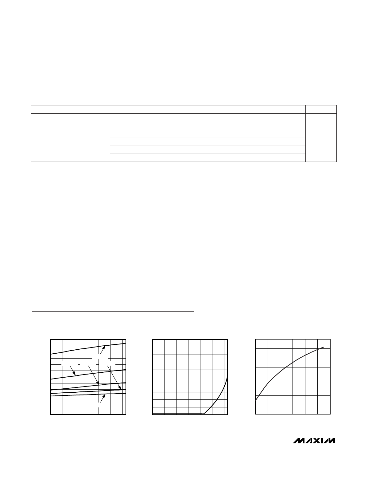
1.0
1.5
2.0
3.0
2.5
3.5
4.0
-40 0-20 20 40 60 80
SUPPLY CURRENT
vs. TEMPERATURE
MAX2605/9-01
TEMPERATURE (°C)
SUPPLY CURRENT (mA)
MAX2609
MAX2605
MAX2606MAX2607MAX2608
0
0.02
0.06
0.04
0.08
0.10
-40 0-20 20 40 60 80
TUNE INPUT LEAKAGE CURRENT
vs. TEMPERATURE
MAX2605/9-02
TEMPERATURE (°C)
LEAKAGE CURRENT (nA)
45
50
55
60
65
0 1.00.5 1.5 2.0 2.5 3.0
MAX2605
VCO TUNING CURVE
MAX2605/9-03
V
TUNE
(V)
FREQUENCY (MHz)
Typical Operating Characteristics
(MAX260_ EV kit, VCC= +2.75V, V
TUNE
= 1.4V, TA = +25°C, unless otherwise noted.)
dBcEven-Order Harmonics -30Differential, RL= 50Ω each side
PARAMETER MIN TYP MAX UNITS
60
CONDITIONS
MAX2605
120
MAX2606
480
MAX2608
220
MAX2607
Supply Pushing (Note 9)
720
kHz/V
MAX2609
Page 5
_______________________________________________________________________________________ 5
MAX2605–MAX2609
45MHz to 650MHz, Integrated IF
VCOs with Differential Output
90
100
110
120
130
0 1.00.5 1.5 2.0 2.5 3.0
MAX2606
VCO TUNING CURVE
MAX2605/9-04
V
TUNE
(V)
FREQUENCY (MHz)
160
180
200
220
240
260
0 1.00.5 1.5 2.0 2.5 3.0
MAX2607
VCO TUNING CURVE
MAX2605/9-05
V
TUNE
(V)
FREQUENCY (MHz)
310
340
370
400
430
0 1.00.5 1.5 2.0 2.5 3.0
MAX2608
VCO TUNING CURVE
MAX2605/9-06
V
TUNE
(V)
FREQUENCY (MHz)
480
520
560
600
640
680
0 1.00.5 1.5 2.0 2.5 3.0
MAX2609
VCO TUNING CURVE
MAX2605/9-07
V
TUNE
(V)
FREQUENCY (MHz)
-50
-40
-30
-20
-10
0
4f
o5fo
2fo3f
o
f
o
6fo7f
o
MAX2605/9-08
FREQUENCY
(dB)
OUTPUT SPECTRUM
NAME FUNCTION
1 IND
Tuning Inductor Port. Connect an inductor from IND to GND to set VCO center frequency (see Oscillation
Frequency).
2 GND Ground. Connect to the ground plane with a low-inductance path.
PIN
3 TUNE Voltage-Control Input for Frequency Tuning. Input voltage range from +0.4V to +2.4V.
4 OUT-
High-Impedance Open-Collector Output. An external pull-up resistor or inductor to VCCis required. Output
power is dependent on external load impedance. OUT- is complementary to OUT+.
6 OUT+
High-Impedance Open-Collector Output. An external pull-up resistor or inductor to VCCis required. Output
power is dependent on external load impedance. OUT+ is complementary to OUT-.
5 V
CC
Supply Voltage Connection. Connect an external bypass capacitor to ground for low noise and low spurious-output content. See Layout Issues for more details.
Pin Description
Typical Operating Characteristics (continued)
(MAX260_ EV kit, VCC= +2.75V, V
TUNE
= 1.4V, TA = +25°C, unless otherwise noted.)
Page 6

MAX2605–MAX2609
45MHz to 650MHz, Integrated IF
VCOs with Differential Output
6 _______________________________________________________________________________________
Detailed Description
The MAX2605–MAX2609 are low-noise VCOs designed
for fixed/single-frequency IF applications. The core
oscillator circuit is based on the well-known Colpitts
topology. The varactor and feedback capacitors are
integrated on-chip so that only an external inductor is
required to establish the frequency of oscillation and
produce a properly operating VCO. The tuning range,
biasing, startup, etc., are all managed within the IC. This
highly integrated design dramatically simplifies the
parts’ application.
The tuning range is wide enough so that, with the use
of ±2% tolerance inductors, no board-level adjustments
to the oscillation frequency are necessary. Once the
correct inductor value is chosen, the VCO is guaranteed always to tune to the desired operating frequency.
In addition, with the use of inductors of moderate Q (35
to 40), the VCO achieves excellent phase-noise performance.
Applications Information
Desired Oscillation Frequency
The desired VCO operating frequency is set by the
value of the external inductance, LF. Figures 1–5 show
the inductance value LFrequired to achieve the desired
oscillation frequency. The inductor value can be taken
directly from these figures. Inductance must be selected accurately to ensure proper operation over all conditions.
Inductor Implementation
The inductance value required for the desired operating frequency may not necessarily coincide with a standard-value SMT inductor, which typically increases size
in ~1.2x steps. In such cases, the inductance must be
constructed from two inductors, L
F1
and LF2, in order to
achieve the desired inductance value. Choose L
F1
to
be a standard-value inductor with a value just less than
that required for L
F
. Choose LF2to be a standard-value
inductor with a value just less than (LF- LF1). L
F1
should adhere to the minimum Q requirements, but L
F2
may be implemented as a lower-cost, lower-Q, thin-film
SMT inductor. Its lower Q has only a small impact on
the overall Q of the total inductance because it is <20%
of the total inductance. However, the overall Q of L
F1
and LF2must be greater than the minimum inductor Q
(Table 1).
It is also permissible to use PC board traces to provide
a small amount of inductance, thereby adjusting the
total inductance value. On the MAX2608/MAX2609, the
inductance values for LF2are sometimes more exactly
implemented as a PC board trace (shorted to GND),
rather than an SMT inductor. When designing LF with
two inductors, use the simple model in Figure 7 to calculate XLand LEQ.
The LFin Figures 1–5 represents an equivalent inductance as seen by pin 1 (IND). The equivalent inductance corresponds to the inductive reactance
connected to IND at the desired oscillation frequency
(f
NOMINAL
).
LEQ= XL/ (2π f
NOMINAL
) as seen in Figure 8
Design LEQ= LFat the desired f
NOMINAL
. The
MAX2605–MAX2609 are designed to tolerate approximately 0.5pF of external parasitic capacitance at IND.
This parasitic capacitance arises from the pad capacitance at the device pin and pads for the inductor.
Additional shunt capacitance is not recommended
because it degrades the tuning range.
Bypass Capacitor on TUNE
The MAX2605–MAX2609’s oscillator design uses a variant of the Colpitts topology, where DC bias for the varactor is applied via a DC voltage on TUNE and a
ground connection through the external inductor L
F
.
TUNE must also have a high-frequency AC ground for
Table 1. External Inductor LFRange
Table 2. C
BYPASS
Values
403.9 ≤ LF≤ 15500 to 650MAX2609
40
35
35
35
MIN
INDUCTOR
Q
10 ≤ LF≤ 47300 to 500MAX2608
39 ≤ LF≤ 180
150 ≤ LF≤ 820
680 ≤ LF≤ 2200
INDUCTANCE
RANGE
(nH)
FREQUENCY
RANGE
(MHz)
45 to 70
70 to 150
150 to 300MAX2607
MAX2606
MAX2605
PART
≥ 39 pFMAX2609
≥ 100 pFMAX2608
≥ 330 pF
≥ 680 pF
≥ 820 pF
C
BYPASS
MAX2607
MAX2606
MAX2605
DEVICE
Page 7

MAX2605–MAX2609
45MHz to 650MHz, Integrated IF
VCOs with Differential Output
_______________________________________________________________________________________ 7
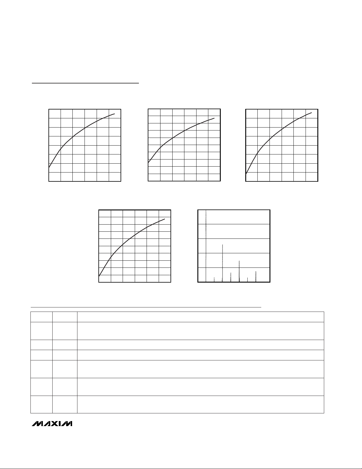
MAX2605
REQUIRED INDUCTANCE vs. DESIRED VCO FIXED FREQUENCY
1900
1800
1700
1600
1500
1400
1300
1200
1100
1000
900
800
700
REQUIRED INDUCTANCE (nH)
45
47
49 51 53 55
57
59 61 63 65 67
69
EFFECTIVE INDUCTANCE
FROM IND TO GND
INDUCTOR VALUE
MOUNTED ON EV KIT
MEASUREMENT CONDITIONS
VCC = 2.75V, TA = 25°C,
R
LOAD
= 100Ω||50Ω (100Ω RESISTIVE PULL-UP PARALLELED WITH 50Ω
VNA IMPEDANCE), UNUSED OUTPUT TERMINATED IN 50Ω,
PCB PARASITIC SHUNT CAPACITANCE (IND TO GND) = 0.45pF
THE INDUCTANCE LISTED IS THE PRECISE NOMINAL INDUCTANCE VALUE
REQUIRED FROM IND TO GND IN ORDER TO GUARANTEE THE VCO
CAN TUNE TO THE DESIRED FIXED FREQUENCY, OVER ALL OPERATING
CONDITIONS AND WORST-CASE COMPONENT
VALUES (±2% INDUCTOR AND IC PROCESS VARIATION).
DESIRED VCO FIXED FREQUENCY (MHz)
Figure 1. MAX2605 Required Inductance vs. Desired VCO Fixed Frequency
Page 8

MAX2605–MAX2609
45MHz to 650MHz, Integrated IF
VCOs with Differential Output
8 _______________________________________________________________________________________
MAX2606
REQUIRED INDUCTANCE vs. DESIRED VCO FIXED FREQUENCY
790
740
690
640
590
540
490
440
390
340
290
240
190
REQUIRED INDUCTANCE (nH)
75
80
85 90 95 100
105
110
115 120 125 130
135
EFFECTIVE INDUCTANCE
FROM IND TO GND
INDUCTOR VALUE
MOUNTED ON EV KIT
140
70 140
145 150
MEASUREMENT CONDITIONS
VCC = 2.75V, TA = 25°C,
R
LOAD
= 100Ω||50Ω (100Ω RESISTIVE PULL-UP PARALLELED WITH 50Ω
VNA IMPEDANCE), UNUSED OUTPUT TERMINATED IN 50Ω,
PCB PARASITIC SHUNT CAPACITANCE (IND TO GND) = 0.45pF
THE INDUCTANCE LISTED IS THE PRECISE NOMINAL INDUCTANCE VALUE
REQUIRED FROM IND TO GND IN ORDER TO GUARANTEE THE VCO
CAN TUNE TO THE DESIRED FIXED FREQUENCY, OVER ALL OPERATING
CONDITIONS AND WORST-CASE COMPONENT
VALUES (±2% INDUCTOR AND IC PROCESS VARIATION).
DESIRED VCO FIXED FREQUENCY (MHz)
Figure 2. MAX2606 Required Inductance vs. Desired VCO Fixed Frequency
Page 9

MAX2605–MAX2609
45MHz to 650MHz, Integrated IF
VCOs with Differential Output
_______________________________________________________________________________________ 9
MAX2607
REQUIRED INDUCTANCE vs. DESIRED VCO FIXED FREQUENCY
160
150
140
130
120
110
100
90
80
70
60
50
40
REQUIRED INDUCTANCE (nH)
160
170
180 190 200 210 220
230
240 250 260 270 280
INDUCTOR VALUE
MOUNTED ON EV KIT
30
150
290
300
170
EFFECTIVE INDUCTANCE
FROM IND TO GND
MEASUREMENT CONDITIONS
VCC = 2.75V, TA = 25°C,
R
LOAD
= 100Ω||50Ω (100Ω RESISTIVE PULL-UP PARALLELED WITH 50Ω
VNA IMPEDANCE), UNUSED OUTPUT TERMINATED IN 50Ω,
PCB PARASITIC SHUNT CAPACITANCE (IND TO GND) = 0.45pF
THE INDUCTANCE LISTED IS THE PRECISE NOMINAL INDUCTANCE VALUE
REQUIRED FROM IND TO GND IN ORDER TO GUARANTEE THE VCO
CAN TUNE TO THE DESIRED FIXED FREQUENCY, OVER ALL OPERATING
CONDITIONS AND WORST-CASE COMPONENT
VALUES (±2% INDUCTOR AND IC PROCESS VARIATION).
DESIRED VCO FIXED FREQUENCY (MHz)
Figure 3. MAX2607 Required Inductance vs. Desired VCO Fixed Frequency
Page 10

MAX2605–MAX2609
45MHz to 650MHz, Integrated IF
VCOs with Differential Output
10 ______________________________________________________________________________________
MAX2608
REQUIRED INDUCTANCE vs. DESIRED VCO FIXED FREQUENCY
40.0
38.0
37.0
32.0
29.0
27.0
25.0
22.0
20.0
17.0
15.0
13.0
11.0
REQUIRED INDUCTANCE (nH)
310 320 330 340 350 360 370 380 390 400 410 420 470
9.0
300 480
41.0
420
430
440 450 460 490 500
36.0
35.0
34.0
33.0
31.0
30.0
28.0
26.0
24.0
23.0
21.0
19.0
18.0
16.0
14.0
12.0
10.0
EFFECTIVE INDUCTANCE
FROM IND TO GND
INDUCTOR VALUE
MOUNTED ON EV KIT
MEASUREMENT CONDITIONS
VCC = 2.75V, TA = 25°C,
R
LOAD
= 100Ω||50Ω (100Ω RESISTIVE PULL-UP PARALLELED WITH 50Ω
VNA IMPEDANCE), UNUSED OUTPUT TERMINATED IN 50Ω,
PCB PARASITIC SHUNT CAPACITANCE (IND TO GND) = 0.45pF
THE INDUCTANCE LISTED IS THE PRECISE NOMINAL INDUCTANCE VALUE
REQUIRED FROM IND TO GND IN ORDER TO GUARANTEE THE VCO
CAN TUNE TO THE DESIRED FIXED FREQUENCY, OVER ALL OPERATING
CONDITIONS AND WORST-CASE COMPONENT
VALUES (±2% INDUCTOR AND IC PROCESS VARIATION).
Figure 4. MAX2608 Required Inductance vs. Desired VCO Fixed Frequency
Page 11

MAX2605–MAX2609
45MHz to 650MHz, Integrated IF
VCOs with Differential Output
______________________________________________________________________________________ 11
MAX2609
REQUIRED INDUCTANCE vs. DESIRED VCO FIXED FREQUENCY
13.5
13.0
11.5
11.0
10.0
9.5
9.0
8.5
7.5
6.5
6.0
5.5
5.0
REQUIRED INDUCTANCE (nH)
510
520
530 540 550 560 570
580
590 600 610 620 630
3.5
500
640
650
14.0
EFFECTIVE INDUCTANCE
FROM IND TO GND
INDUCTOR VALUE
MOUNTED ON EV KIT
12.5
12.0
10.5
8.0
7.0
4.5
4.0
DESIRED VCO FIXED FREQUENCY (MHz)
MEASUREMENT CONDITIONS
VCC = 2.75V, TA = 25°C,
R
LOAD
= 100Ω||50Ω (100Ω RESISTIVE PULL-UP PARALLELED WITH 50Ω
VNA IMPEDANCE), UNUSED OUTPUT TERMINATED IN 50Ω,
PCB PARASITIC SHUNT CAPACITANCE (IND TO GND) = 0.45pF
THE INDUCTANCE LISTED IS THE PRECISE NOMINAL INDUCTANCE VALUE
REQUIRED FROM IND TO GND IN ORDER TO GUARANTEE THE VCO
CAN TUNE TO THE DESIRED FIXED FREQUENCY, OVER ALL OPERATING
CONDITIONS AND WORST-CASE COMPONENT
VALUES (±2% INDUCTOR AND IC PROCESS VARIATION).
Figure 5. MAX2609 Required Inductance vs. Desired VCO Fixed Frequency
Page 12

MAX2605–MAX2609
45MHz to 650MHz, Integrated IF
VCOs with Differential Output
12 ______________________________________________________________________________________
the cathode of the varactor. This is accomplished
through the use of a simple bypass capacitor connected from TUNE to ground. The value of this capacitor
should be greater than or equal to the values listed in
Table 2.
This capacitor provides an AC “short” to ground for the
internal node of the varactor. It is acceptable to select
the next-largest standard-value capacitor. Use a
capacitor with a low-loss dielectric such as NPO; X7Rbased capacitors are not suitable. Omitting this capacitor would affect the tuning characteristics of the
MAX2605–MAX2609. Proper operation of the VCOs
requires the use of this bypass capacitor.
The MAX2605–MAX2609 VCO is designed to tune over
the full tuning range with a voltage range of 0.4V to
2.4V applied to TUNE. This voltage typically originates
from the output of the phase-locked (PLL) loop filter.
Output Interface
The MAX2605–MAX2609 VCO includes a differential
output amplifier after the oscillator core. The amplifier
stage provides valuable isolation and offers a flexible
interface to the IF stages, such as a mixer and PLL
prescaler. The output can be taken single ended or differentially; however, the maximum output power and
lowest harmonic output are achieved in the differential
output mode.
Both outputs (OUT- and OUT+) are open-collector
types and require a pull-up element to VCC; this can be
either resistive or inductive. A resistor pull-up is the
most straightforward method of interfacing to the output, and works well in applications that operate at lower
frequencies or only require a modest voltage swing.
In Figure 6, Z1 and Z2 are 1kΩ pull-up resistors that are
connected from OUT+ and OUT- to VCC, respectively.
These resistors provide DC bias for the output amplifier
and are the maximum value permitted with compliance
to the output voltage swing limits. In addition, the 1kΩ
resistors maximize the swing at the load. DC-blocking
capacitors are connected from OUT- and OUT+ to the
load. If the load driven is primarily resistive and the
VCO operating frequency is below the -3dB bandwidth
of the output network, then the peak-to-peak differential
signal amplitude is approximately:
To optimize the output voltage swing or the output
power, use a reactive power match. The matching network is a simple shunt-inductor series-capacitor circuit,
as shown in Figure 6. The inductors are connected
from OUT- and OUT+ (in place of resistors) to VCCto
provide DC bias for the output stage. The series capacitors are connected from OUT- and OUT+ to the load.
The values for L
MATCH(Z1
and Z2) and C
MATCH(C1
and C2) are chosen according to the operating frequency and load impedance. As the output stage is
essentially a high-speed current switch, traditional linear impedance using techniques with [S] parameters
do not apply. To achieve a reactive power match, start
with the component values provided in the EV kit, and
adjust values experimentally.
In general, the differential output may be applied in any
manner, as would conventional differential outputs. The
only constraints are the need for a pull-up element to
VCCand a voltage swing limit at the output pins OUTand OUT+.
Layout Considerations
In general, a properly designed PC board is essential
to any RF/microwave circuit or system. Always use controlled impedance lines (microstrip, coplanar waveguide, etc.) on high-frequency signals. Always place
decoupling capacitors as close to the VCCpin as possible. For low phase noise and spurious content, use an
appropriate size decoupling capacitor. For long V
CC
lines, it may be necessary to add additional decoupling
capacitors located further from the device. Always provide a low-inductance path to ground. Keep the GND
vias as close to the device as possible. In addition, the
VCO should be placed as far away from the noisy section of a larger system, such as a switching regulator or
digital circuits. Use star topology to separate the
ground returns.
The resonator tank circuit (LF) is critical in determining
the VCO’s performance. For best performance, use
high-Q components and choose values carefully. To
minimize the effects of parasitic elements, which
degrade circuit performance, place L
F
and C
BYP
close
to their respective pins. Specifically, place C
BYP
direct-
ly across pins 2 (GND) and 3 (TUNE).
For the higher frequency versions, consider the extra
parasitic inductance and capacitance when determining the oscillation frequency. Be sure to account for the
following: PC board pad capacitance at IND, PC board
pad capacitance at the junction of two series inductors,
series inductance of any PC board traces, and the
inductance in the ground return path from the grounded side of the inductor and IC’s GND pin. For best
results, connect the “ground” side to the tuning inductor as close to pin 2 as possible. In addition, remove
the ground plane around and under LFand C
BYP
to
minimize the effects of parasitic capacitance.
V diff 2 1mA
1k R
1k R
OUTp p
LOAD
LOAD
−
()
=×
×
+
Ω
Ω
Page 13

MAX2605–MAX2609
45MHz to 650MHz, Integrated IF
VCOs with Differential Output
______________________________________________________________________________________ 13
Chip Information
TRANSISTOR COUNT: 158
C1
C3
R
LOAD
R
LOAD
C2
Z2
Z1
OUT-
TUNE
FROM PLL LOOP
FILTER OUTPUT
1
6
OUT+
5
V
CC
L
F
C
BYP
MAX2605
MAX2606
MAX2607
MAX2608
MAX2609
2
34
V
CC
Figure 6. Typical Operating Circuit
Page 14

MAX2605–MAX2609
45MHz to 650MHz, Integrated IF
VCOs with Differential Output
14 ______________________________________________________________________________________
IND
MAX2605
MAX2606
MAX2607
MAX2608
MAX2609
1
L
F2
C
PAR1
L
F1
C
PAR2
Figure 7. Simple Model of External Inductance
IND
MAX2605
MAX2606
MAX2607
MAX2608
MAX2609
1
LEQ = XL / 2π ƒ
NOMINAL
X
L
Figure 8. Inductive Reactance at Pin 1 (IND)
MAX2605
MAX2606
MAX2607
MAX2608
MAX2609
4
Z
L
V
CC
Γ
Figure 9. Output Matching Network
Page 15

Package Information
6LSOT.EPS
Maxim cannot assume responsibility for use of any circuitry other than circuitry entirely embodied in a Maxim product. No circuit patent licenses are
implied. Maxim reserves the right to change the circuitry and specifications without notice at any time.
Maxim Integrated Products, 120 San Gabriel Drive, Sunnyvale, CA 94086 408-737-7600 _____________________15
© 2002 Maxim Integrated Products Printed USA is a registered trademark of Maxim Integrated Products.
45MHz to 650MHz, Integrated IF
VCOs with Differential Output
 Loading...