

General Description
The MAX2601/MAX2602 are RF power transistors optimized for use in portable cellular and wireless equipment
that operates from three NiCd/NiMH cells or one Li-Ion
cell. These transistors deliver 1W of RF power from a
3.6V supply with efficiency of 58% when biased for constant-envelope applications (e.g., FM or FSK). For NADC
(IS-54) operation, they deliver 29dBm with -28dBc ACPR
from a 4.8V supply.
The MAX2601 is a high-performance silicon bipolar RF
power transistor. The MAX2602 includes a highperformance silicon bipolar RF power transistor, and a
biasing diode that matches the thermal and process
characteristics of the power transistor. This diode is
used to create a bias network that accurately controls
the power transistor’s collector current as the temperature changes.
The MAX2601/MAX2602 can be used as the final stage
in a discrete or module power amplifier. Silicon bipolar
technology eliminates the need for voltage inverters
and sequencing circuitry, as required by GaAsFET
power amplifiers. Furthermore, a drain switch is not
required to turn off the MAX2601/MAX2602. This
increases operating time in two ways: it allows lower
system end-of-life battery voltage, and it eliminates the
wasted power from a drain-switch device.
The MAX2601/MAX2602 are available in thermally
enhanced, 8-pin SO packages, which are screened to
the extended temperature range (-40°C to +85°C).
________________________Applications
Narrow-Band PCS (NPCS)
915MHz ISM Transmitters
Microcellular GSM (Power Class 5)
AMPS Cellular Phones
Digital Cellular Phones
Two-Way Paging
CDPD Modems
Land Mobile Radios
____________________________Features
♦♦
Low Voltage: Operates from 1 Li-Ion or
3 NiCd/NiMH Batteries
♦♦
DC-to-Microwave Operating Range
♦♦
1W Output Power at 900MHz
♦♦
On-Chip Diode for Accurate Biasing (MAX2602)
♦♦
Low-Cost Silicon Bipolar Technology
♦♦
Does Not Require Negative Bias or Supply Switch
♦♦
High Efficiency: 58%
MAX2601/MAX2602
3.6V, 1W RF Power Transistors
for 900MHz Applications
________________________________________________________________
Maxim Integrated Products
1
19-1185; Rev 3; 9/08
For pricing, delivery, and ordering information, please contact Maxim Direct at 1-888-629-4642,
or visit Maxim’s website at www.maxim-ic.com.
Ordering Information
Typical Application Circuit appears at end of data sheet.
PART TEMP RANGE PIN-PACKAGE
MAX2601ESA -40°C to +85°C 8 SOIC
MAX2602ESA -40°C to +85°C 8 SOIC
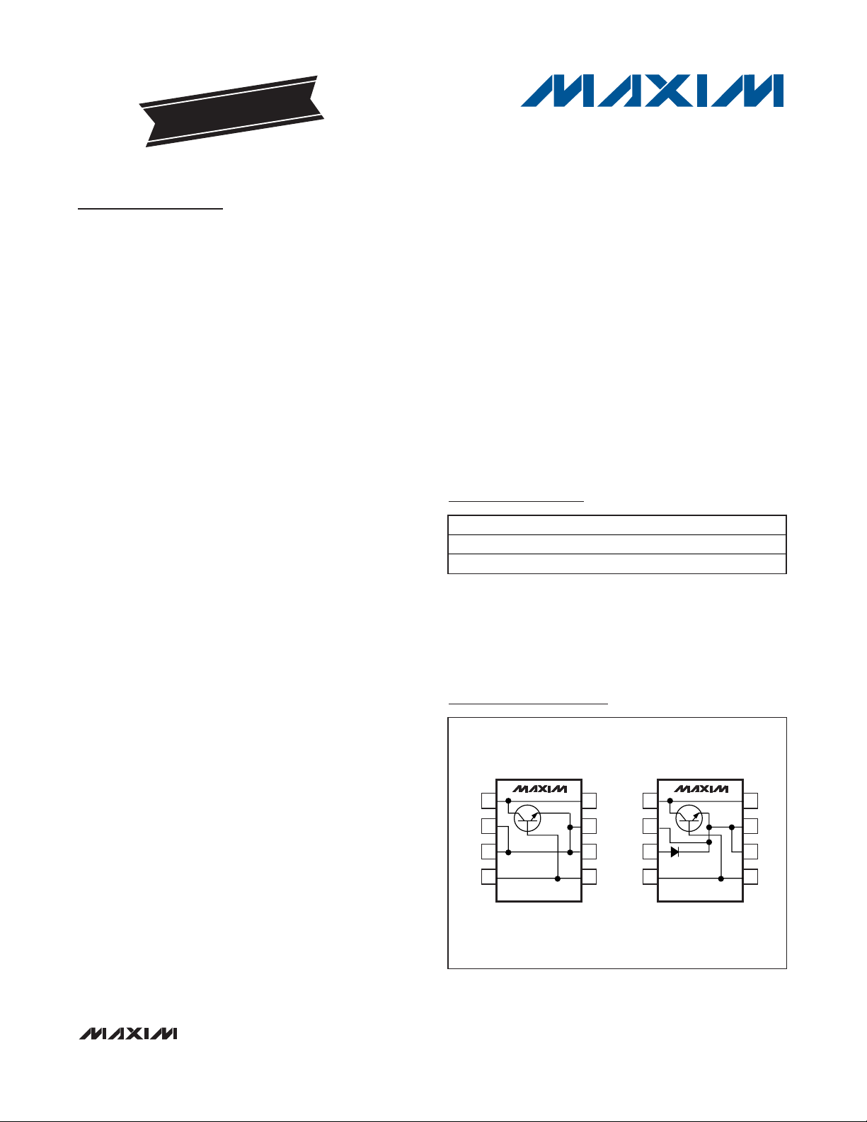
Pin Configurations
PSOPII
TOP VIEW
PSOPII
8
7
6
5
1
2
3
4
C
E
E
B
C
E
E
B
MAX2602
8
7
6
5
1
2
3
4
C
E
BIAS
B
C
E
E
B
MAX2601
EVALUATION KIT
AVAILABLE
dBc
MAX2601/MAX2602
3.6V, 1W RF Power Transistors
for 900MHz Applications
2 _______________________________________________________________________________________
ABSOLUTE MAXIMUM RATINGS
DC ELECTRICAL CHARACTERISTICS
(TA= T
MIN
to T
MAX
, unless otherwise noted.)
Stresses beyond those listed under “Absolute Maximum Ratings” may cause permanent damage to the device. These are stress ratings only, and functional
operation of the device at these or any other conditions beyond those indicated in the operational sections of the specifications is not implied. Exposure to
absolute maximum rating conditions for extended periods may affect device reliability.
Collector-Emitter Voltage, Shorted Base (V
CES
) ....................17V
Emitter Base Reverse Voltage (V
EBO
)...................................2.3V
BIAS Diode Reverse Breakdown Voltage (MAX2602) ..........2.3V
Average Collector Current (I
C
)........................................1200mA
Continuous Power Dissipation (T
A
= +70°C)
SOIC (derate 80mW/°C above +70°C) (Note 1) .............6.4W
Operating Temperature Range ...........................-40°C to +85°C
Storage Temperature Range .............................-65°C to +165°C
Junction Temperature......................................................+150°C
Lead Temperature (soldering, 10s) .................................+300°C
I
C
< 100µA
V5.0LV
CEO
Collector-Emitter Sustaining
Voltage
V
15BV
CES
15BV
CEO
Collector-Emitter Breakdown
Voltage
100h
FE
DC Current Gain
µA0.05 1.5I
CES
Collector Cutoff Current
pF9.6C
OB
Output Capacitance
UNITSMIN TYP MAXSYMBOLPARAMETER
Note 1: Backside slug must be properly soldered to ground plane (see
Slug Layout Techniques
section).
IC= 200mA
Shorted base
Open base
IC= 250mA, VCE= 3V
VCE= 6V, VBE= 0V
VCB= 3V, IE= 0mA, f = 1MHz
CONDITIONS
dB3.3NFNoise Figure
dBc
-25IM5
Two-Tone IMR
-16IM3
8:1V
SWR
Stability under Continuous
Load Mismatch Conditions
%58
η
Collector Efficiency
dB11.6Power Gain
-42
2fo, 3foHarmonics
-43
mA4.2I
B
Base Current
GHzDC 1fFrequency Range
UNITSMIN TYP MAXSYMBOLPARAMETER
VBB= 0.9V
P
OUT
= +30dBm total power, f1 = 835MHz,
f2 = 836MHz
VCC= 3.6V, P
OUT
= 30dBm
VCC= 5.5V, all angles (Note 3)
(Note 2)
No modulation
P
OUT
= 30dBm
CONDITIONS
AC ELECTRICAL CHARACTERISTICS
(Test Circuit of Figure 1, VCC= 3.6V, VBB= 0.750V, Z
LOAD
= Z
SOURCE
= 50Ω, P
OUT
= 30dBm, f = 836MHz, TA= +25°C, unless oth-
erwise noted.)
Note 2: Guaranteed by design.
Note 3: Under these conditions: a) no spurious oscillations shall be observed at collector greater than -60dBc; b) no parametric
degradation is observable when mismatch is removed; and c) no current draw in excess of the package dissipation
capability is observed.
V15BV
CBO
Collector-Base Breakdown
Voltage
IC< 100µA, emitter open
VCC= 3.0V, P
OUT
= 29dBm
dBc

MAX2601/MAX2602
3.6V, 1W RF Power Transistors
for 900MHz Applications
_______________________________________________________________________________________ 3
ACPR
(dB
)
__________________________________________Typical Operating Characteristics
(Test Circuit of Figure 1, input/output matching networks optimized for specific measurement frequency, VCC= 3.6V, VBB= 0.750V,
P
OUT
= 30dBm, Z
LOAD
= Z
SOURCE
= 50Ω, f = 836MHz, TA= +25°C, unless otherwise noted.)
NAME
—
1, 8 C Transistor Collector
2, 3, 6, 7, Slug E Transistor Emitter
BIAS
4, 5 B Transistor Base
Anode of the Biasing Diode that matches the thermal and process characteristics of the power transistor. Requires a high-RF-impedance, lowDC-impedance (e.g., inductor) connection to the transistor base (Pin 4).
Current through the biasing diode (into Pin 3) is proportional to 1/15 the
collector current in the transistor.
FUNCTION
MAX2601 MAX2602
3
1, 8
2, 6, 7, Slug
PIN
4, 5
______________________________________________________________Pin Description
1.0
0.8
0.6
(A)
CC
I
0.4
0.2
, IM3, IM5 (dBm)
OUT
P
0
06
TWO-TONE OUTPUT POWER, IM3, IM5
vs. INPUT POWER (f = 433MHz)
35
25
P
, IM3, AND IM5
OUT
ARE RMS COMPOSITE
15
TWO-TONE
POWER LEVELS
5
-5
5
COLLECTOR CURRENT
VBB = 1.00V
VBB = 0.95V
VBB = 0.85V
VBB = 0.80V
24513
VCE (V)
P
OUT
IM3
IM5
15 2510 20
INPUT POWER (dBm)
TWO-TONE OUTPUT POWER AND IM3
vs. COLLECTOR CURRENT
31
P
, IM3, AND IM5
OUT
VBB = 0.90V
MAX2601-01
ARE RMS COMPOSITE
TWO-TONE POWER LEVELS
30
(dBm)
29
OUT
P
28
27
0.4
0.6 0.80.5 0.7
ICC (A)
P
OUT
MAX2601-02
IM3
ACPR vs. OUTPUT POWER
4.8V
= 0.85V)
BB
4.2V
MAX2601-05
(IS-54 π/4 DQPSK MODULATION, V
-20
-22
MAX2601-04
-24
-26
c
-28
-30
-32
-34
-36
-38
-40
10
OUTPUT POWER (dBm)
3.0V
3.6V
20 3515 25 30
20
19
18
17
16
TWO-TONE OUTPUT POWER, IM3, IM5
vs. INPUT POWER
35
P
, IM3, AND IM5
OUT
ARE RMS COMPOSITE
TWO-TONE POWER
LEVELS
25
15
, IM3, IM5 (dBm)
OUT
P
5
-5
5
INPUT POWER (dBm)
P
OUT
IM3
IM5
15 2510 20
COLLECTOR EFFICIENCY vs. OUTPUT POWER
(IS-54 π/4 DQPSK MODULATION, V
60
P
, IM3, AND IM5
OUT
ARE RMS COMPOSITE
50
TWO-TONE POWER
LEVELS
40
30
EFFICIENCY (%)
20
10
0
10
3.0V
3.6V
20 3515 25 30
OUTPUT POWER (dBm)
4.2V
4.8V
= 0.85V)
BB
MAX2601-03
MAX2601-06

MAX2601/MAX2602
3.6V, 1W RF Power Transistors
for 900MHz Applications
4 _______________________________________________________________________________________
_______________Detailed Description
MAX2601/MAX2602
The MAX2601/MAX2602 are high-performance silicon
bipolar transistors in power-enhanced, 8-pin SO packages. The base and collector connections use two pins
each to reduce series inductance. The emitter connects
to three (MAX2602) or four (MAX2601) pins in addition
to a back-side heat slug, which solders directly to the
PC board ground to reduce emitter inductance and
improve thermal dissipation. The transistors are intended to be used in the common-emitter configuration for
maximum power gain and power-added
efficiency.
Current Mirror Bias
(MAX2602 only)
The MAX2602 includes a high-performance silicon
bipolar RF power transistor and a thermally matched
biasing diode that matches the power transistor’s thermal and process characteristics. This diode is used to
create a bias network that accurately controls the
power transistor’s collector current as the temperature
changes (Figure 2).
The biasing diode is a scaled version of the power transistor’s base-emitter junction, in such a way that the
current through the biasing diode is 1/15 the quiescent
collector current of the RF power transistor. Supplying
the biasing diode with a constant current source and
connecting the diode’s anode to the RF power transistor’s base ensures that the RF power transistor’s quiescent collector current remains constant through
temperature variations. Simply tying the biasing diode
to the supply through a resistor is adequate in most situations. If large supply variations are anticipated, connect the biasing diode to a reference voltage through a
resistor, or use a stable current source. Connect the
biasing diode to the base of the RF power transistor
through a large RF impedance, such as an RF choke
(inductor), and decouple to ground through a surfacemount chip capacitor larger than 1000pF.
Figure 1. Test Circuit
Figure 2. Bias Diode Application
V
BB
0.1μF
RF
IN
2pF
=
COILCRAFT A05T INDUCTOR, 18.5nH
L1
T1, T2 =
1", 50Ω TRANSMISSION LINE ON FR-4
1000pF
T1
5Ω
1000pF
100nH
12pF
24Ω
4
5
2, 6, 7
BACKSIDE
SLUG
V
CC
0.1μF1000pF
L1
1
8
1000pF
10pF
T2
2pF
V
CC
R
BIAS
RF
C
Q1
C
BIAS
RF
C
IN
IN
V
CC
RF
C
RF
OUT
C
OUT
Q2

MAX2601/MAX2602
3.6V, 1W RF Power Transistors
for 900MHz Applications
_______________________________________________________________________________________ 5
Applications Information
Optimum Port Impedance
The source and load impedances presented to the
MAX2601/MAX2602 have a direct impact upon its gain,
output power, and linearity. Proper source- and loadterminating impedances (ZSand ZL) presented to the
power transistor base and collector will ensure optimum
performance.
For a power transistor, simply applying the conjugate of
the transistor’s input and output impedances calculated
from small-signal S-parameters will yield less than optimum device performance.
For maximum efficiency at V
BB
= 0.75V and VCC=
3.6V, the optimum power-transistor source and load
impedances (as defined in Figure 3) are:
At 836MHz: ZS= 5.5 + j2.0
Z
L
= 6.5 + j1.5
At 433MHz: Z
S
= 9.5 - j2.5
ZL= 8.5 - j1.5
ZSand ZLreflect the impedances that should be presented to the transistor’s base and collector. The package parasitics are dominated by inductance (as shown
in Figure 3), and need to be accounted for when calculating ZSand ZL.
The internal bond and package inductances shown
in Figure 3 should be included as part of the endapplication matching network, depending upon exact
layout topology.
Slug Layout Techniques
The most important connection to make to the
MAX2601/MAX2602 is the back side. It should connect
directly to the PC board ground plane if it is on the top
side, or through numerous plated through-holes if the
ground plane is buried. For maximum gain, this connection should have very little self-inductance. Since it
is also the thermal path for heat dissipation, it must
have low thermal impedance, and the ground plane
should be large.
Figure 3. Optimum Port Impedance
Package Information
For the latest package outline information and land patterns, go
to www.maxim-ic.com/packages
.
PACKAGE TYPE PACKAGE CODE DOCUMENT NO.
8 SOIC S8E-12
21-0041
1234
Z
S
MAX2601
MAX2602
2.8nH
2.8nH
Z
L
8765
2.8nH
2.8nH

MAX2601/MAX2602
3.6V, 1W RF Power Transistors
for 900MHz Applications
Maxim cannot assume responsibility for use of any circuitry other than circuitry entirely embodied in a Maxim product. No circuit patent licenses are
implied. Maxim reserves the right to change the circuitry and specifications without notice at any time.
6
_____________________Maxim Integrated Products, 120 San Gabriel Drive, Sunnyvale, CA 94086 408-737-7600
© 2008 Maxim Integrated Products Maxim is a registered trademark of Maxim Integrated Products, Inc.
Revision History
REVISION
NUMBER
REVISION
DATE
DESCRIPTION
PAGES
CHANGED
2 5/97 — —
3 9/08 Removed die version from Ordering Information 1
 Loading...