

Page 1
General Description
The MAX256 is an integrated primary-side controller
and H-bridge driver for isolated power-supply circuits.
The device contains an on-board oscillator, protection
circuitry and internal FET drivers to provide up to 3W of
power to the primary winding of a transformer. The
MAX256 can be operated using the internal programmable oscillator or can be driven by an external clock
for improved EMI performance. Regardless of the clock
source being used, an internal flip-flop stage guarantees a fixed 50% duty cycle to prevent DC current flow
in the transformer.
The MAX256 operates from a single-supply voltage of
+5V or +3.3V, and includes undervoltage lockout for
controlled startup. The device prevents cross-conduction of the H-bridge MOSFETs by implementing breakbefore-make switching. Thermal shutdown circuitry
provides additional protection against damage due to
overtemperature conditions.
The MAX256 is available in the 8-pin thermally-enhanced
SO package. The device is specified for the automotive
(-40°C to +125°C) temperature range.
Applications
Features
o Provides Up to 3W to the Transformer in Isolated
Power Supplies
o Single Supply +5V or +3.3V Operation
o Internal Resistor-Programmable Oscillator Mode
o External Clock Mode with Watchdog
o Disable Mode
o Undervoltage Lockout
o Thermal Shutdown
MAX256
3W Primary-Side Transformer H-Bridge Driver
for Isolated Supplies
________________________________________________________________
Maxim Integrated Products
1
19-3748; Rev 1; 3/12
For pricing, delivery, and ordering information, please contact Maxim/Dallas Direct! at
1-888-629-4642, or visit Maxim’s website at www.maxim-ic.com.
EVALUATION KIT
AVAILABLE
GND
ST2MODE
1
+
2
87ST1
GND
V
CC
V
CC
CK_RS
3
4
6
5
*EP
SO-EP
*CONNECT EXPOSED PAD TO GND.
MAX256
Pin Configuration
Ordering Information
*
EP = Exposed paddle.
*
/V denotes an automotive qualified part.
+
Denotes a lead(Pb)-free/RoHS-compliant package.
T = Tape and reel.
Isolated Power Supplies
Industrial Process
Control
Isolated Communications
Links
Medical Equipment
Telecommunications
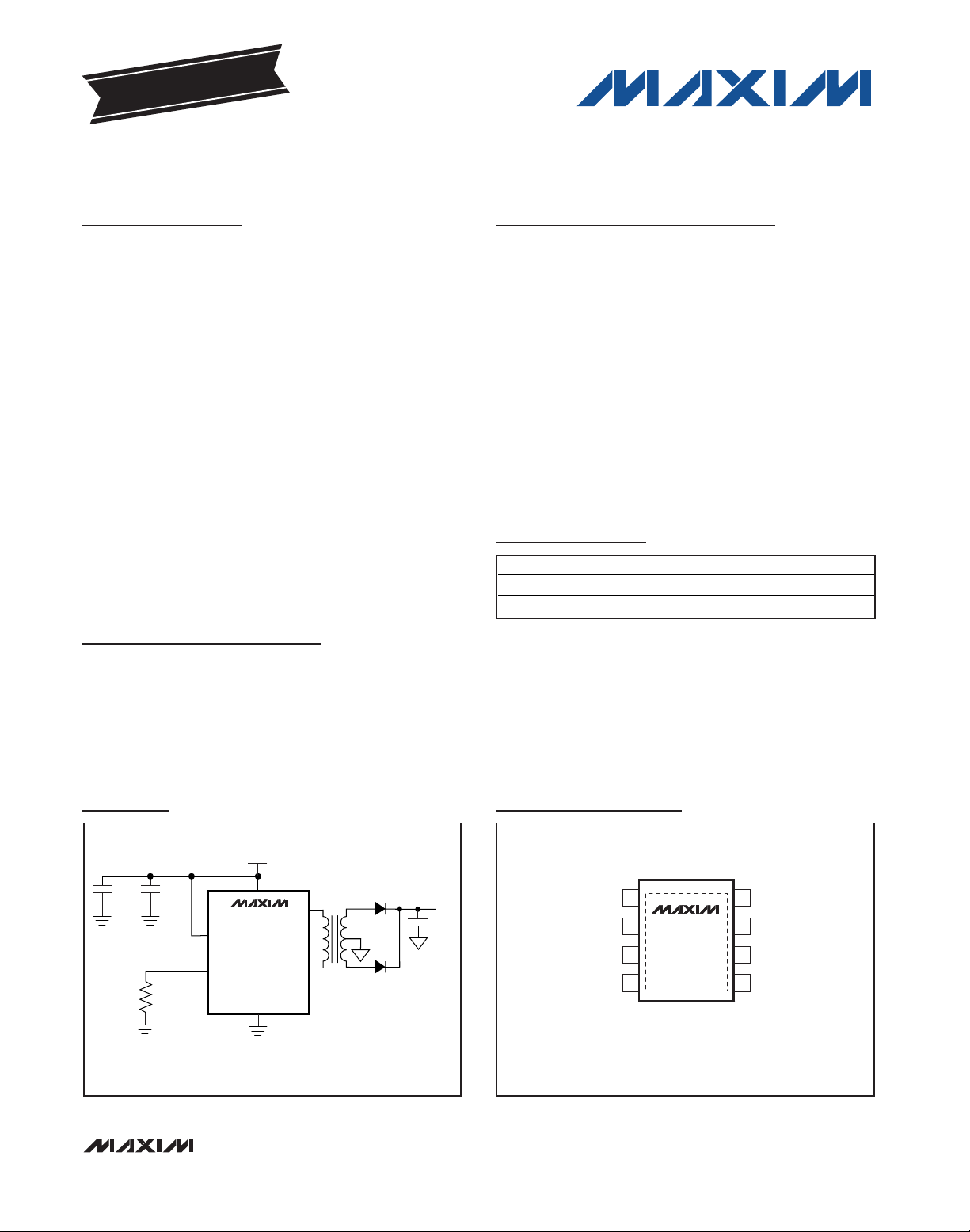
Typical Application Circuit
PART TEMP RANGE PIN-PACKAGE
MAX256ASA+ - 40°C to +125°C 8 SO-EP*
MAX256ASA/V+T - 40°C to +125°C 8 SO-EP*
4.7µF
47kΩ
+5V
470nF
MAX256
MODE
CK_RS
GND
+5V TO ISOLATED +5V TYPICAL APPLICATION
ST2
ST1
1:2.6CT
+5V ISOLATED
µF
0.1
Page 2
MAX256
3W Primary-Side Transformer H-Bridge Driver
for Isolated Supplies
2 _______________________________________________________________________________________
ABSOLUTE MAXIMUM RATINGS
Stresses beyond those listed under “Absolute Maximum Ratings” may cause permanent damage to the device. These are stress ratings only, and functional
operation of the device at these or any other conditions beyond those indicated in the operational sections of the specifications is not implied. Exposure to
absolute maximum rating conditions for extended periods may affect device reliability.
(All voltages referenced to GND, unless otherwise noted.)
Supply Voltage V
CC
..................................................-0.3V to +6V
ST1, ST2, CK_RS, MODE (Note 1)................-0.3V to V
CC
+ 0.3V
ST1, ST2 Maximum Continuous Current (T
A
< +125°C) ....±0.6A
ST1, ST2 Maximum Continuous Current (T
A
< +100°C) ....±0.9A
ST1, ST2 Maximum Continuous Current (T
A
< +85°C) ......±1.0A
Continuous Power Dissipation (T
A
= +70°C)
8-Pin SO (derate 18.9mW/°C above +70°C)..............1509mW
Operating Temperature Range .........................-40°C to +125°C
Storage Temperature Range .............................-65°C to +150°C
Junction Temperature......................................................+150°C
Lead Temperature (soldering, 10s) .................................+300°C
Soldering Temperature (reflow) .......................................+260°C
DC ELECTRICAL CHARACTERISTICS
(VCC= +3.0V to +5.5V, TA= T
MIN
to T
MAX
. Typical values are at VCC= +5.0V and TA= +25°C, unless otherwise noted.)
Note 1: ST1 and ST2 are not protected against short circuits. Damage to the device may result from a short-circuit fault.
SO-EP
Junction-to-Ambient Thermal Resistance (θ
JA
)...............53°C/W
Junction-to-Case Thermal Resistance (θ
JC
)......................5°C/W
Note 2: Package thermal resistances were obtained using the method described in JEDEC specification JESD51-7, using a four-
layer board. For detailed information on package thermal considerations, refer to www.maxim-ic.com/thermal-tutorial
.
PACKAGE THERMAL CHARACTERISTICS (Note 2)
PARAMETER SYMBOL CONDITIONS MIN TYP MAX UNITS
Supply Voltage V
Supply Current I
Disable Supply Current I
External Resistance Range R
Driver Total Resistance R
Undervoltage Lockout Threshold V
Undervoltage-Lockout-Threshold
Hysteresis
Logic-Low Level
(MODE, CK_RS)
Logic-High Level
(MODE, CK_RS)
Input Leakage Current
(MODE)
Internal Pulldown Resistance on
CK_RS
Thermal Shutdown T
Thermal Shutdown Hysteresis T
CC
CC
SD
OHL
UVLO
V
UVLO_HST
V
V
I
LK
R
S_INT
SHDN
SHDN_HST
M OD E = V
MODE = GND,
CK_RS unconnected
S
VCC = 4.5V (Note 4) 0.5 1.0
VCC = 3.0V (Note 4) 0.6 1.2
VCC rising 0.8 1.9 2.7 V
VCC = 4.5V 0.8
IL
VCC = 3.0V 0.7
IH
MODE = GND 165 kΩ
3.0 5.5 V
C K_RS unconnected ( N ote 3) 1.06 3 mA
C C ,
50 µA
10 kΩ
110 mV
2.0 V
1µA
165 °C
10 °C
Ω
V
Page 3
MAX256
3W Primary-Side Transformer H-Bridge Driver
for Isolated Supplies
_______________________________________________________________________________________ 3
TIMING CHARACTERISTICS
(VCC= +3.0V to +5.5V, TA= T
MIN
to T
MAX
. Typical values are at VCC= +5.0V and TA= +25°C, unless otherwise noted.)
Note 3: Minimum and maximum limits tested with ST1, ST2 unconnected.
Note 4: Total driver resistance includes the on-resistance of the top and the bottom internal FETs. If R
OH
is the high-side resistance,
and R
OL
is the low-side resistance, R
OHL
= ROH+ ROL.
Pin Description
PARAMETER SYMBOL CONDITIONS MIN TYP MAX UNITS
Switching Frequency f
CK_RS Input Frequency f
ST1 and ST2 Duty Cycle Dtc MODE = V
Crossover Dead Time t
Watchdog Timeout t
PIN NAME FUNCTION
1 CK_RS
Clock Input/Oscillator Frequency Adjust. When MODE is HIGH, set the internal oscillator frequency by
connecting a 10kΩ or greater resistor from CK_RS to ground. When MODE is LOW, apply an external
clock signal to CK_RS. The MAX256 outputs switch at one half the external clock frequency.
SW
IN
DEAD
WDOG
MODE = VCC, RS = 10.5kΩ 0.75 1 1.35 MHz
MODE = V
MODE = GND 0.2 2 MHz
RL = 100Ω 20 ns
MODE = GND 20 55 µs
CK_RS unconnected 65 100 160 kHz
CC,
CC
49 50 51 %
2, 3 V
4 MODE
5 ST2 Transformer Drive Output 2
6, 7 GND Ground
8 ST1 Transformer Drive Output 1
—EP
CC
VCC Supply Voltage, +3.0V ≤ VCC ≤ +5.5V.
Bypass V
Mode Control Input. Drive MODE high to enable internal oscillator. Drive MODE low and supply a valid
clock signal on CK_RS for external clock mode.
EP is internally connected to GND. Connect to a large ground plane to maximize thermal
performance; not intended as an electrical connection point.
to ground with a 4.7µF capacitor and a 470nF ceramic capacitor.
CC
Page 4
MAX256
3W Primary-Side Transformer H-Bridge Driver
for Isolated Supplies
4 _______________________________________________________________________________________
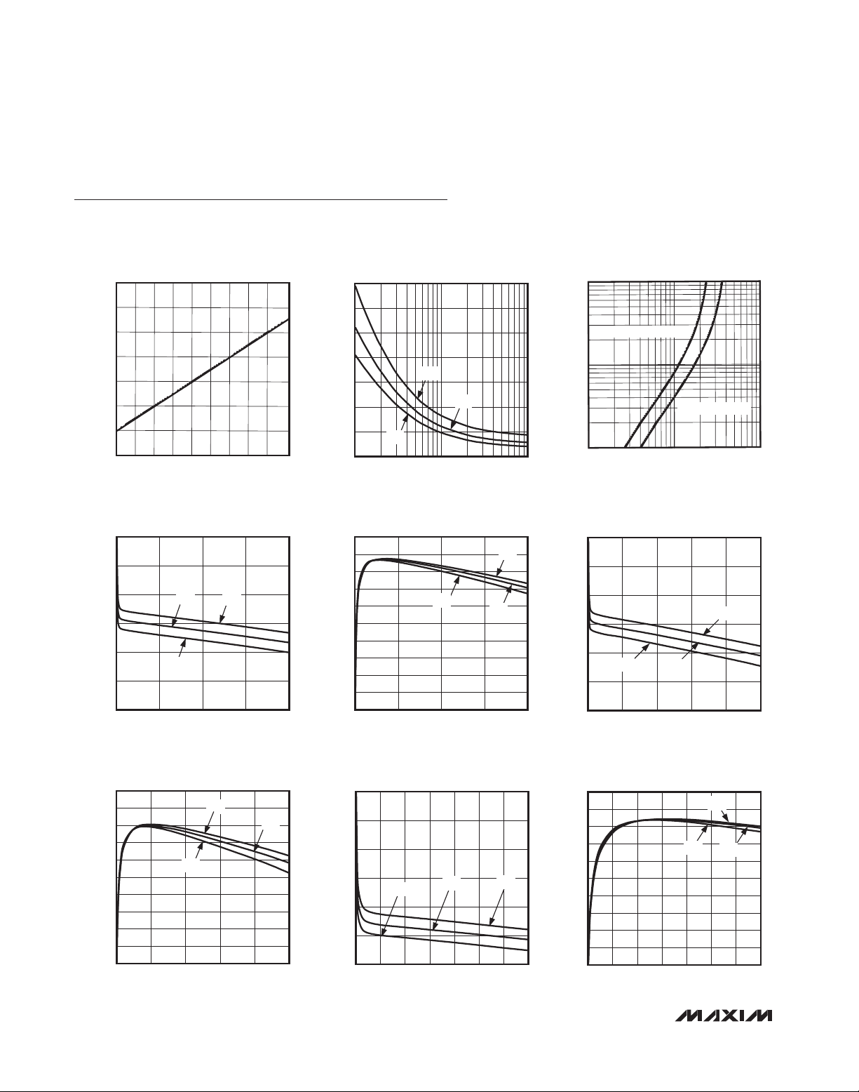
Typical Operating Characteristics
(VCC= +5.0V ±10%, TA= +25°C, unless otherwise noted.) (See
Figure 8
)
SUPPLY CURRENT vs.
OSCILLATOR FREQUENCY
MAX256toc01
OSCILLATOR FREQUENCY (kHz)
SUPPLY CURRENT (mA)
900
400
2
3
4
5
6
7
1
100
0
200 300 500 600 700 800 1000
OSCILLATOR FREQUENCY vs. RS (+1%)
RS (kΩ)
OSCILLATOR FREQUENCY (kHz)
MAX256 toc02
0
200
400
600
800
1000
1200
1400
10 100 1000
MAX
TYP
MIN
OUTPUT VOLTAGE vs. OUTPUT CURRENT
(TYPICAL APPLICATION FIGURE 9)
OUTPUT CURRENT (mA)
OUTPUT VOLTAGE (V)
MAX256 toc06
0 100 200 300 400 500
0
2
4
6
8
10
12
3.0V
3.6V
3.3V
OUTPUT VOLTAGE vs. OUTPUT CURRENT
(TYPICAL APPLICATION FIGURE 8)
12
10
8
6
4
OUTPUT VOLTAGE (V)
2
0
0 200 400 600 800
OUTPUT CURRENT (mA)
4.5V
5.0V
5.5V
MAX256 toc04
EFFICIENCY vs. OUTPUT CURRENT
(TYPICAL APPLICATION FIGURE 8)
1.0
0.9
0.8
0.7
0.6
0.5
0.4
EFFICIENCY
0.3
0.2
0.1
0
0 200 400 600 800
4.5V
OUTPUT CURRENT (mA)
5.0V
5.5V
MAX256 toc05
(kΩ)
S
R
1000
100
RS vs. REQUIRED ET PRODUCT
+3.6V MAX SUPPLY
10
REQUIRED ET PRODUCT (Vµs)
+5.5V MAX SUPPLY
10
MAX256toc03
1001
EFFICIENCY vs. OUTPUT CURRENT
(CIRCUIT OF FIGURE 9)
1.0
0.9
0.8
0.7
0.6
0.5
0.4
EFFICIENCY
0.3
0.2
0.1
0
0 100 200 300 400 500
3.6V
3.0V
OUTPUT CURRENT (mA)
3.3V
MAX256 toc07
OUTPUT VOLTAGE (V)
OUTPUT VOLTAGE vs. OUTPUT CURRENT
(CIRCUIT OF FIGURE 10)
40
35
30
25
20
15
10
4.5V
0 20 40 60 80 100 120 140
OUTPUT CURRENT (mA)
5.0V
5.5V
MAX256 toc08
EFFICIENCY vs. OUTPUT CURRENT
(CIRCUIT OF FIGURE 10)
1.0
0.9
0.8
0.7
0.6
0.5
0.4
EFFICIENCY
0.3
0.2
0.1
0
0 20 40 60 80 100 120 140
OUTPUT CURRENT (mA)
4.5V
5.5V
MAX256 toc09
5.0V
Page 5
MAX256
3W Primary-Side Transformer H-Bridge Driver
for Isolated Supplies
_______________________________________________________________________________________
5
Typical Operating Characteristics (continued)
(VCC= +5.0V ±10%, TA= +25°C, unless otherwise noted.) (See
Figure 8
)
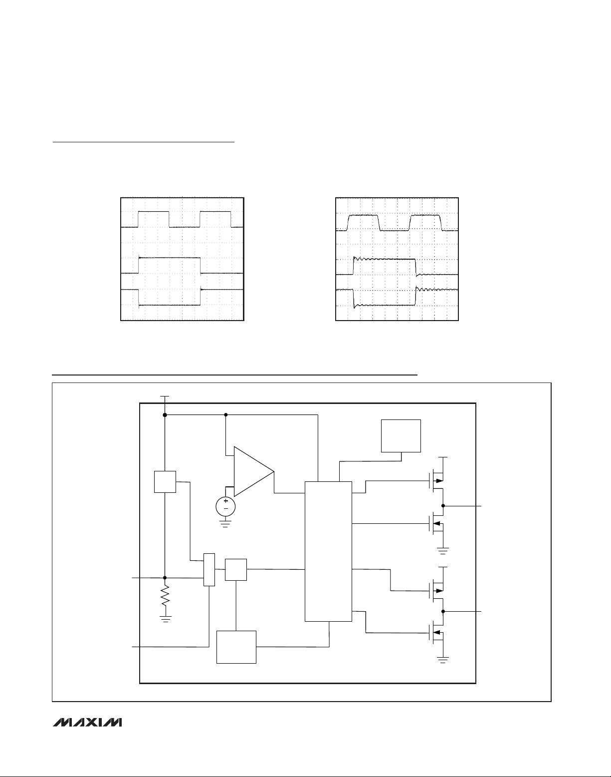
Functional Diagram
OPERATION AT 100kHz
MAX256toc10
CK_RS
5V/div
ST1
5V/div
ST2
5V/div
1µs/div
V
CC
OPERATION WITH
EXTERNAL 2MHz CLOCK
MAX256toc11
CK_RS
5V/div
ST1
5V/div
ST2
5V/div
100ns/div
CK_RS
MODE
OSC
165kΩ
M
U
X
UVLO
V
FLIPFLOP
WATCHDOG
UVLO
MOSFET
H-BRIDGE
DRIVER
THERMAL
SHUTDOWN
V
CC
ST1
V
CC
ST2
Page 6

MAX256
Detailed Description
The MAX256 is an integrated primary-side controller
and H-bridge driver for isolated power-supply circuits.
The device contains an on-board oscillator, protection
circuitry, and internal FET drivers to provide up to 3W of
power to the primary winding of a transformer. The
MAX256 can be operated using the internal programmable oscillator, or can be driven by an external clock
for improved EMI performance. Regardless of the clock
source being used, an internal flip-flop stage guarantees a fixed 50% duty cycle to prevent DC current flow
in the transformer.
The MAX256 operates from a single-supply voltage of
+5V or +3.3V, and includes undervoltage lockout for
controlled startup. The device prevents cross-conduction of the H-bridge MOSFETs by implementing breakbefore-make switching. Thermal shutdown circuitry
provides additional protection against damage due to
overtemperature conditions.
Oscillator Modes
The MAX256 is driven by the internal programmable
oscillator or an external clock. The logic state of MODE
determines the clock source (see Table 1). Drive
MODE high to select the internal resistor programmable
oscillator. Drive MODE low to operate the MAX256 with
an external clock signal on CK_RS.
Internal Oscillator Mode
The MAX256 includes a 100kHz to 1MHz programmable oscillator. Set the oscillator frequency by connecting CK_RS to ground with a 10kΩ or larger resistor.
Leave CK_RS unconnected to set the oscillator to the
minimum default frequency of 100kHz. CK_RS is internally pulled to ground with a 165kΩ resistor.
External Clock Mode
The MAX256 provides an external clock mode. When
operating in external clock mode, an internal flip-flop
divides the external clock by two in order to generate a
switching signal with a guaranteed 50% duty cycle. As
a result, the MAX256 outputs switch at one half the
external clock frequency. The device switches on the
rising edge of the external clock signal.
Watchdog
When the MAX256 is operating in external clock mode,
a stalled clock could cause excessive DC current to
flow through the primary winding of the transformer.
The MAX256 features an internal watchdog circuit to
prevent damage from this condition. The MAX256 is
disabled when the external clock signal on CK_RS
remains at the same logic level for longer than 55µs
(max). The device resumes normal operation upon the
next rising edge on CK_RS.
Disable Mode
When using the internal oscillator, drive MODE low to
disable the MAX256. The device is disabled within
55µs after MODE goes low. When operating in external
clock mode, suspend the clock signal for longer than
55µs to disable the MAX256. The device resumes normal operation when MODE is driven high or when the
external clock signal resumes.
Power-Up and Undervoltage Lockout
The MAX256 provides an undervoltage lockout feature
to ensure a controlled power-up state and prevent
operation before the oscillator has stabilized. On
power-up and during normal operation (if the supply
voltage drops below 1.8V), the undervoltage lockout
disables the device.
Thermal Shutdown
The MAX256 is protected from overtemperature damage by a thermal shutdown circuit. When the junction
temperature (TJ) exceeds +165°C, the device is disabled. The device resumes normal operation when T
J
falls below +155°C.
ESD Protection
As with all Maxim devices, ESD-protection structures
are incorporated on all pins to protect against electrostatic discharges encountered during handling and
assembly.
ESD Test Conditions
ESD performance depends on a variety of conditions.
Please contact Maxim for a reliability report documenting test setup, methodology, and results.
3W Primary-Side Transformer H-Bridge Driver
for Isolated Supplies
6 _______________________________________________________________________________________
Page 7

Applications Information
Available Output Power
With a supply voltage of +5V over the extended -40°C to
+85°C temperature range, the MAX256 is specified to
provide up to 3W of power to the primary side of a transformer in an isolated power supply. The device provides
up to 2.5W of power to the primary winding over the
+85°C to +125°C temperature range. The output power
is specified at ST1 and ST2 since losses in the transformer and rectification network are dependent upon
component selection and topology. The power dissipation of the MAX256 is approximated by:
where R
OHL
is the total high-side and low-side on-resis-
tance of the internal FET drivers, and I
PRI
is the load
current flowing through the transformer primary between
ST1 and ST2. For low output load currents, include the
contribution to PDfrom the quiescent supply current:
ICCx VCC.
PC Board Layout Guidelines
As with all power-supply circuits, careful PC board layout is important to achieve low switching losses and stable operation. For thermal performance, connect the
exposed paddle to a solid copper ground plane.
The traces from ST1 and ST2 to the transformer must be
low-resistance and inductance paths. Place the transformer as close as possible to the MAX256 using short,
wide traces.
When the device is operating with the internal oscillator,
it is possible for high-frequency switching components
on ST1 and ST2 to couple into the CK_RS circuitry
through PC board parasitic capacitance. This capacitive
coupling can induce duty-cycle errors in the oscillator,
resulting in a DC current through the transformer. To
ensure proper operation, shield the CK_RS circuitry
MAX256
3W Primary-Side Transformer H-Bridge Driver
for Isolated Supplies
_______________________________________________________________________________________ 7
Table 1. Oscillator Modes
Figure 1. Secondary-Side Rectification Topologies
OSCILLATOR
MODE
Internal
Programmable
Frequency
External Clock
Disable
Unconnected or pulled to ground by R
be greater than 10kΩ.
Digital input. Drive CK_RS with an external clock
signal.
Connected to VCC or GND
(external clock mode)
Unconnected or pulled to ground with R
(internal clock mode)
CK_RS MODE OPERATION
S
PR I
=×
D OHL PRI
2
. RS must
S
V
CC
Ground
Ground
V
V
V
100kHz to 1MHz (typ).
Leave CK_RS unconnected for minimum
switching frequency.
CK_RS is pulled to ground by an internal
165kΩ resistor. The device switches at one
half the external clock frequency.
The device is disabled after a maximum of
55µs following the last rising edge on
CK_RS.
1:N CT
+
IN
-
FIGURE 1A. PUSH-PULL RECTIFICATION
1:N
+
IN
-
FIGURE 1B. VOLTAGE DOUBLER
1:N
+
IN
-
FIGURE 1C. FULL-WAVE RECTIFIER
+
V
= N / 2 * VIN - V
OUT
-
V
= DIODE FORWARD VOLTAGE
D
+
V
-
+
V
-
D
= 2(NVIN - V
OUT
= NVIN - 2V
OUT
)
D
D
Page 8

MAX256
from ST1 and ST2 by placing a grounded trace between
these circuits. Place R
S
as close as possible to the
CK_RS pin. An additional capacitance of 100nF from
CK_RS to GND may be required in some applications.
Output Voltage Regulation
For many applications, the unregulated output of the
MAX256 meets the supply voltage tolerances. This configuration represents the highest efficiency possible
with the MAX256.
For applications requiring a regulated output voltage,
Maxim provides several solutions. In the following
examples, assume a tolerance of ±10% variation for the
input voltage.
When a full-bridge power supply is operated under
maximum input voltage and low output load current, the
voltage at the output of the rectifier network can exceed
the absolute maximum input voltage of the low dropout
regulator (LDO). If the minimum output load current is
less than approximately 5mA, connect a zener diode
from the output voltage to ground (as shown in Figure
2) to limit the output to a safe value.
+3.3V to Isolated, Regulated +5.0V
In the circuit of Figure 2, the MAX1659 LDO regulates
the output of the MAX256 to +5V. The Halo TGMH281NF provides a center-tapped 1:2.6 turns ratio, and
the secondary circuit implements a 4-diode bridge rectifier (Figure 1C).
For a minimum input voltage of +3.0V, the output voltage of the bridge rectifier is approximately +5.5V at a
current of 200mA. A 15V zener diode protects the LDO
from high input voltages, but adds a few microamps to
the no-load input current of the MAX256.
+5V to Isolated, Regulated +3.3V
In Figure 3, the MAX1658 LDO is used with the TGMH281NF transformer and a 2-diode push-pull rectifier
(Figure 1A). This topology produces approximately
+4.5V at a current of 350mA. The MAX1658 produces a
regulated +3.3V output voltage.
+5V to Isolated, Regulated +12V
In Figure 4, the 7812 LDO is used with the TGMH281NF transformer and the voltage doubler network
(Figure 1B). This circuit produces approximately
+12.5V at a load current of 150mA. The 7812 produces
a regulated +12V output.
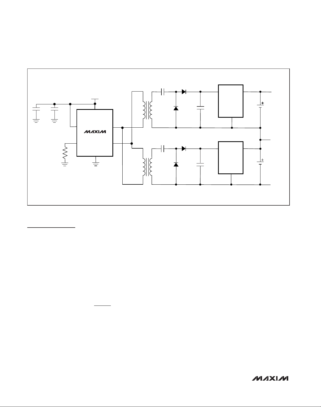
+5V to Isolated, Regulated ±15V
In Figure 5, the MAX256 is used with two TGM-280NS
transformers and voltage doubler networks (Figure 1B)
to supply 20V to a pair of 7815 regulators. The circuit
produces a regulated ±15V at 50mA.
Isolated DAC/ADC Interface for Industrial
Process Control
The MAX256 provides isolated power for data converters in industrial process control applications (Figure 6).
The 3W isolated power output capability allows for data
converters operating across multiple isolation barriers.
The power output capability also supports circuitry for
signal conditioning and multiplexing.
Isolated RS-485/RS-232 Data Interfaces
The MAX256 provides power for multiple transceivers in
isolated RS-485/RS-232 data interface applications. The
3W isolated power output capability of the MAX256
allows more than ten RS-485 transceivers simultaneously.
Isolated Power Supply
The MAX256 allows a versatile range of secondary-side
rectification circuits (see Figure 1). The secondary
transformer winding can be wound to provide a wide
range of isolated voltages. The MAX256 delivers 3W of
power to the transformer with a +5V supply (-40°C to
+85°C). The MAX256 produces up to 2.5W over the
+85°C to +125°C temperature range. For a supply voltage of +3.3V, the MAX256 delivers 2W of power to the
transformer over the -40°C to +85°C temperature
range, and 1.4W between +85°C and +125°C. Figure 8
shows a +5V to isolated +5V application that delivers
up to 500mA. In Figure 9, the MAX256 is configured to
provide +5V from a +3.3V supply at 350mA, and in
Figure 10, the MAX256 provides isolated +15V and 15V at a total current up to 75mA.
The MAX256 provides the advantages of the full-bridge
converter topology, including multiple isolated outputs,
step-up/step-down or inverted output, relaxed filtering
requirements, and low output ripple.
Power-Supply Decoupling
Bypass VCCto ground with a 0.47µF ceramic capacitor
as close to the device as possible. Additionally, place a
4.7µF capacitor from VCCto ground.
Exposed Paddle
Ensure that the exposed paddle is soldered to the bottom layer ground for best thermal performance. Failure
to provide a low thermal impedance path to the ground
plane will result in excessive junction temperatures
when delivering maximum output power.
3W Primary-Side Transformer H-Bridge Driver
for Isolated Supplies
8 _______________________________________________________________________________________
Page 9

MAX256
3W Primary-Side Transformer H-Bridge Driver
for Isolated Supplies
_______________________________________________________________________________________ 9
Figure 2. +3.3V to Isolated Regulated +5V
Figure 3. +5V to Isolated Regulated +3.3V
Figure 4. +5V to Isolated Regulated +12V
+3.3V
4.7µF
470nF
MAX256
MODE
CK_RS
300kΩ
4.7µF
470nF
MODE
CK_RS
100kΩ
V
CC
GND
+5V
V
CC
MAX256
GND
TGM-H281NF
ST1
ST2
TGM-H281NF
ST1
ST2
MBRS140 x 4
MBRS140
0.1µF
MBRS140
0.1µF
15V
15V
MAX1659
MAX1658
10µF
10µF
+
5V
-
+
3.3V
-
4.7µF
470nF
MAX256
MODE
CK_RS
100kΩ
+5V
V
GND
CC
TGM-H281NF
ST1
0.1µF
MBRS140
0.1µF
7812
10µF
+
12V
-
ST2
MBRS140
Page 10
MAX256
Component Selection
Transformer Selection
Transformer selection for the MAX256 can be simplified
by the use of a design metric, the ET product. The ET
product relates the maximum allowable magnetic flux
density in a transformer core to the voltage across a
winding and switching period. Inductor current in the
primary linearly increases with time in the operating
region of the MAX256. Transformer manufacturers
specify a minimum ET product for each transformer. For
the MAX256, the requirement on ET product is calculated as:
By choosing a transformer with sufficient ET product in
the primary winding, it is ensured that the transformer
will not saturate during operation. Saturation of the
magnetic core results in significantly reduced inductance of the primary, and therefore a large increase in
current flow. Excessive transformer current results in a
temperature rise and possible damage to the transformer and/or the MAX256.
When CK_RS is unconnected, the internal oscillator is
programmed for the minimum frequency. The default
required ET product for the MAX256 is 42.3Vµs, (assuming +5.5V maximum VCC), or 27.7Vµs for +3.3V operation (assuming +3.6V maximum VCC). Both of these ET
products assume the minimum oscillator frequency of
65kHz. See the
Typical Operating Characteristics
plot,
R
S
vs. Required ET Product to determine the required
ET product for a given value of R
S
.
In addition to the constraint on ET product, choose a
transformer with a low DC-winding resistance. Power
dissipation of the transformer due to the copper loss is
approximated as:
where R
PRI
is the DC-winding resistance of the primary,
and R
SEC
is the DC-winding resistance of the sec-
ondary. In most cases, an optimum is reached when:
For this condition, the power dissipation is equal for the
primary and secondary windings.
3W Primary-Side Transformer H-Bridge Driver
for Isolated Supplies
10 ______________________________________________________________________________________
Figure 5. +5V to Isolated Regulated ±15V
+5V
4.7µF
47kΩ
470nF
MODE
CK_RS
V
CC
MAX256
GND
ST1
ST2
TGM-280NS
TGM-280NS
MBRS140
+15V
0.1µF
0.1µF
MBRS140
MBRS140
0.1µF
0.1µF
MBRS140
7815
7815
10µF
COMMON
10µF
-15V
ET V
=×
CC
f
×12
SW
PI NRR
=× +
D TX LOAD PRI SEC_
2
2
⎛
⎝
RNR
SEC PRI
2
=
⎞
⎠
Page 11

As with all power-supply designs, it is important to optimize efficiency. In designs incorporating small transformers, the possibility of thermal runaway makes low
transformer efficiencies problematic. Transformer losses produce a temperature rise that reduces the efficiency of the transformer. The lower efficiency, in turn,
produces an even larger temperature rise.
To ensure that the transformer meets these requirements under all operating conditions, the design should
focus on the worst-case conditions. The most stringent
demands on ET product arise for minimum switching
frequency, maximum input voltage, maximum temperature, and load current. Additionally, the worst-case values for transformer and rectifier losses should be
considered.
The primary should be a single winding; however, the
secondary can be center-tapped, depending on the
desired rectifier topology. In most applications, the
phasing between primary and secondary windings is
not significant. Half-wave rectification architectures are
possible with the MAX256; however, these are discouraged. If a net DC current results due to an imbalanced
load, the magnetic flux in the core is increased. This
reduces the effective ET product and can lead to saturation of the transformer core.
Transformers for use with the MAX256 are typically
wound on a high-permeability magnetic core. To minimize radiated electromagnetic emissions, select a
toroid, pot core, E/I/U core, or equivalent.
+3.3V Operation
The MAX256 can be operated from a +3.3V supply by
increasing the turns ratio of the transformer, or by
designing a voltage-doubler or voltage-tripler circuit as
shown in Figure 1B.
Optimum performance at +3.3V is obtained with fewer
turns on the primary winding, since the ET product
is lower than for a +5V supply. However, any of the
transformers for use with a +5V supply will operate
properly with a +3.3V supply. For a given power level,
the transformer currents are higher with a +3.3V supply
than with a +5V supply. Therefore, the DC resistance
of the transformer windings has a larger impact on the
circuit efficiency.
MAX256
3W Primary-Side Transformer H-Bridge Driver
for Isolated Supplies
______________________________________________________________________________________ 11
Figure 6. Isolated Power Supply for Process Control Applications
V
CC
+15V
MAX256
COMMON
V
CC
RS485
MPU
OPTOISOLATORS
-15V
M
U
X
OPTOISOLATORS
DAC/ADC
Page 12

MAX256
Low-Power Applications and Multiple Transformers
For more information about transformer selection, please
refer to the MAX3535E data sheet. The MAX3535E uses a
transformer in a similar topology. See Tables 3, 4, and 5
in the MAX3535E data sheet for a list of commercially
available transformers. These transformers are preferred
for lower power applications and are suitable for use with
the MAX256 up to the power limits of the transformers.
Alternatively, the MAX256 can drive the primaries of two
or more low-power transformers to provide multiple isolated outputs. One or more of the manufacturers listed in the
MAX3535E data sheet may produce a custom transformer for specific applications. Contact the individual
transformer suppliers for details.
Diode Selection
The high switching speed of the MAX256 necessitates
high-speed rectifiers. Ordinary silicon signal diodes
such as 1N914 or 1N4148 may be used for low-output
current levels (less than 50mA). At higher output currents, select low forward-voltage Schottky diodes to
improve efficiency. Ensure that the average forward
current rating for the rectifier diodes exceeds the maximum load current of the circuit. For surface-mount
applications, Schottky diodes such as the BAT54,
MBRS140 and MBRS340 are recommended.
Capacitor Selection
Input Bypass Capacitor
Bypass the supply voltage to GND with a 0.47µF
ceramic capacitor as close to the device as possible.
Additionally, connect a 4.7µF or greater capacitor to
provide input voltage filtering. The equivalent series
resistance (ESR) of the input capacitors is not as critical as for the output capacitors. Typically, ceramic X7R
capacitors are adequate.
Output Filter Capacitor
In most applications, the actual capacitance rating of the
output filter capacitor is less critical than the capacitor's
ESR. In applications sensitive to output voltage ripple,
the output filter capacitor must have low ESR. For optimal
performance, the capacitance should meet or exceed
the specified value over the entire operating temperature
range. Capacitor ESR typically rises at low temperatures;
however, OS-CON capacitors can be used at temperatures below 0°C to help reduce output voltage ripple in
sensitive applications. In applications where low outputvoltage ripple is not critical, standard ceramic 0.1µF
capacitors are sufficient.
3W Primary-Side Transformer H-Bridge Driver
for Isolated Supplies
12 ______________________________________________________________________________________
Figure 7. Output Ripple Filter
Figure 8. +5V to Isolated +5V
Figure 9. +3.3V to Isolated +5V
Figure 10. +5V to Isolated ±15V
4.7µF
470nF
47kΩ
4.7µF
470nF
MODE
CK_RS
47kΩ
25µH
MODE
CK_RS
+3.3V
MAX256
GND
L1
+5V
MAX256
GND
ST1
ST2
FILTER
OUTPUT
C1
2.2µF
ST1
ST2
1:2
1:2.6CT
+5V ISOLATED
0.1
+5V
ISOLATED
0.1
ALL DIODES
MBRS140
+5V
4.7µF
47kΩ
470nF
MAX256
MODE
CK_RS
GND
1:1.75
ST1
ST2
µF
0.1
µF
0.1
+5V ISOLATED
µF
0.1
µF
0.1
-15V ISOLATED
ALL DIODES
MBRS140
µF
µF
Page 13

Output-Ripple Filtering
Output voltage ripple can be reduced with a lowpass
LC pi-filter (Figure 7). The component values shown
give a cutoff frequency of 21.5kHz by the equation:
Use an inductor with low DC resistance and sufficient saturation current rating to minimize filter power dissipation.
MAX256
3W Primary-Side Transformer H-Bridge Driver
for Isolated Supplies
______________________________________________________________________________________ 13
Table 2. Suggested External Component Manufacturers
Chip Information
PROCESS: BiCMOS
Package Information
For the latest package outline information and land patterns
(footprints), go to www.maxim-ic.com/packages
. Note that a
“+”, “#”, or “-” in the package code indicates RoHS status only.
Package drawings may show a different suffix character, but
the drawing pertains to the package regardless of RoHS status.
PACKAGE
TYPE
PACKAGE
CODE
OUTLINE NO.
LAND
PATTERN NO.
8 SO-EP S8E+12
21-0111
90-0150
MANUFACTURER COMPONENT WEBSITE PHONE
Central Semiconductor diodes www.centralsemi.com 631-435-1110
Halo Electronics transformers www.haloelectronics.com 650-903-3800
Kemet capacitors www.kemet.com 864-963-6300
Sanyo capacitors www.sanyo.com 619-661-6835
Taiyo Yuden capacitors www.t-yuden.com 408-573-4150
TDK capacitors www.component.tdk.com 888-835-6646
2=π
1
LC
f
dB3
Page 14

MAX256
3W Primary-Side Transformer H-Bridge Driver
for Isolated Supplies
Maxim cannot assume responsibility for use of any circuitry other than circuitry entirely embodied in a Maxim product. No circuit patent licenses are
implied. Maxim reserves the right to change the circuitry and specifications without notice at any time. The parametric values (min and max limits) shown in
the Electrical Characteristics table are guaranteed. Other parametric values quoted in this data sheet are provided for guidance.
14
____________________Maxim Integrated Products, 120 San Gabriel Drive, Sunnyvale, CA 94086 408-737-7600
© 2012 Maxim Integrated Products Maxim is a registered trademark of Maxim Integrated Products, Inc.
Revision History
REVISION
NUMBER
0 8/05 Initial release —
1 3/12
REVISION
DATE
DESCRIPTION
Added automotive-qualified part information. Added lead-free packaging
information
PAGES
CHANGED
1–4, 8, 12
 Loading...