

Page 1
_______________General Description
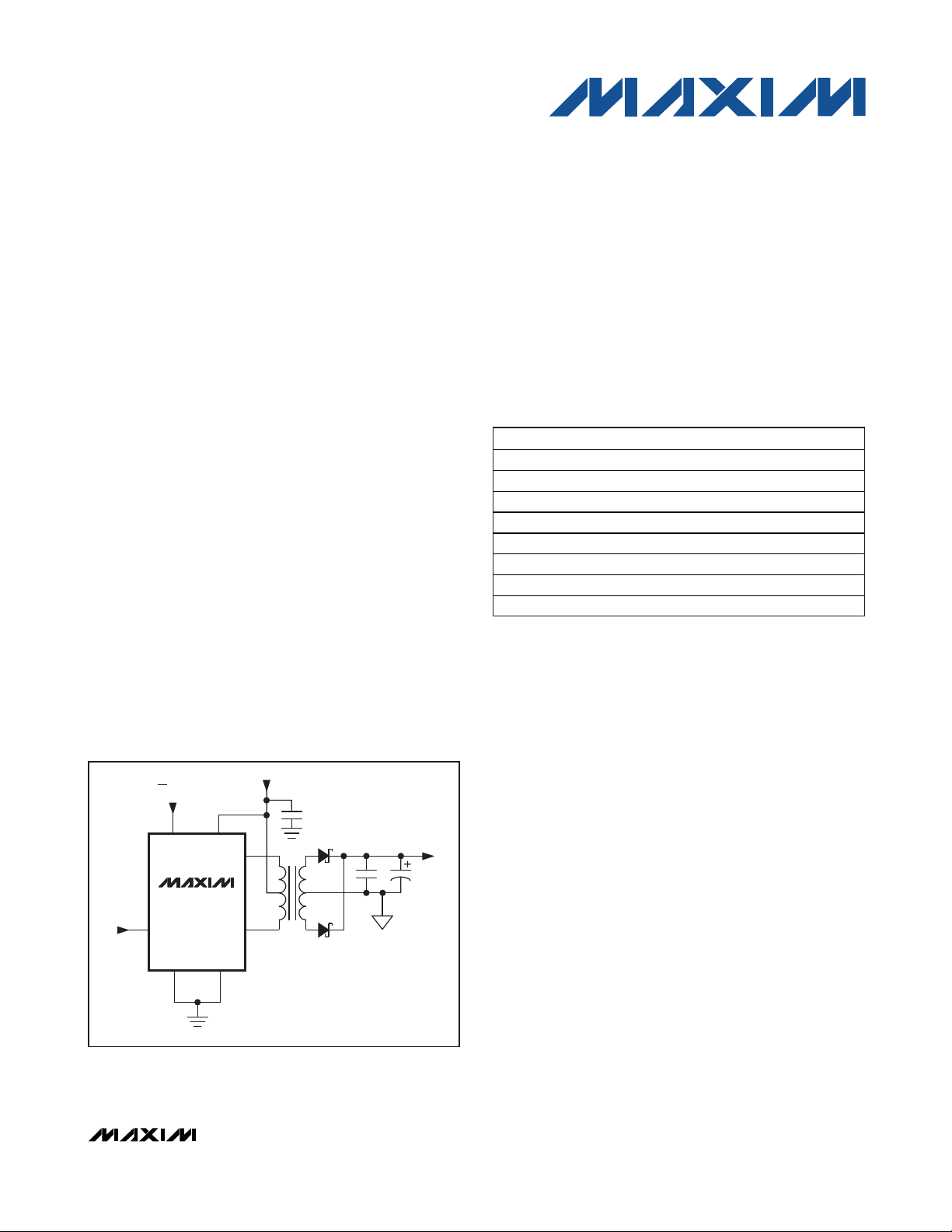
The MAX253 monolithic oscillator/power-driver is
specifically designed to provide isolated power for an
isolated RS-485 or RS-232 data interface. The device
drives a center-tapped transformer primary from a 5V
or 3.3V DC power supply. The secondary can be
wound to provide any isolated voltage needed at power
levels up to 1W.
The MAX253 consists of a CMOS oscillator driving a
pair of N-channel power switches. The oscillator runs
at double the output frequency, driving a toggle flip-flop
to ensure 50% duty cycle to each of the switches.
Internal delays are arranged to ensure break-beforemake action between the two switches.
The SD pin puts the entire device into a low-power
shutdown state, disabling both the power switches and
oscillator.
________________________Applications
Isolated RS-485/RS-232 Power-Supply
Transformer Driver
High Noise-Immunity Communications Interface
Isolated and/or High-Voltage Power Supplies
Bridge Ground Differentials
Medical Equipment
Process Control
____________________________Features
♦♦
Power-Supply Transformer Driver for Isolated
RS-485/RS-232 Data-Interface Applications
♦♦
Single 5V or 3.3V Supply
♦♦
Low-Current Shutdown Mode: 0.4µA
♦♦
Pin-Selectable Frequency: 350kHz or 200kHz
♦♦
8-Pin DIP, SO, and µMAX
®
Packages
______________Ordering Information
MAX253
Transformer Driver for
Isolated RS-485 Interface
________________________________________________________________
Maxim Integrated Products
1
__________Typical Operating Circuit
19-0226; Rev 2; 4/10
For pricing, delivery, and ordering information, please contact Maxim Direct at 1-888-629-4642,
or visit Maxim’s website at www.maxim-ic.com.
*
Contact factory for dice specifications.
**
Contact factory for availability and processing to MIL-STD-883.
Devices are also available in a lead(Pb)-free/RoHS-compliant
package. Specify lead-free by adding a (+) to the part number
when ordering.
/V Denotes an automotive qualified part.
µMAX is a registered trademark of Maxim Integrated Products, Inc.
PART TEMP RANGE PIN-PACKAGE
MAX253CP A 0°C to +70°C 8 Plastic DIP
MAX253CS A 0°C to +70°C 8 SO
MAX253CU A 0°C to +70°C 8 μMAX
MAX253C/D 0°C to +70°C Dice*
MAX253EPA -40°C to +85°C 8 Plastic DIP
MAX253ESA -40°C to +85°C 8 SO
MAX253ESA/V -40°C to +85°C 8 SO
MAX253MJA -55°C to +125°C 8 CERDIP**
V
5V
ON / OFF
46
SD
MAX253
3
FREQUENCY
SWITCH
GND1 GND2
27
IN
C1
OUTPUT
C3
5V @ 200mA
C2
V
CC
1
D1
8
D2FS
Page 2
MAX253
Transformer Driver for
Isolated RS-485 Interface
2 _______________________________________________________________________________________
ABSOLUTE MAXIMUM RATINGS
ELECTRICAL CHARACTERISTICS
(VCC= 5V ±10%, TA= T
MIN
to T
MAX
, unless otherwise noted. Typical values are at TA= +25°C.)
Stresses beyond those listed under “Absolute Maximum Ratings” may cause permanent damage to the device. These are stress ratings only, and functional
operation of the device at these or any other conditions beyond those indicated in the operational sections of the specifications is not implied. Exposure to
absolute maximum rating conditions for extended periods may affect device reliability.
Note 1: Operating supply current is the current used by the MAX253 only, not including load current.
Note 2: Shutdown supply current includes output switch-leakage currents.
PARAMETER
MIN TYP MAX UNITS
Shutdown Input Threshold
0.8 µA
2.4 V
Shutdown Supply Current (Note 2) 0.4 µA
Operating Supply Current (Note 1) 0.45 5.0 mA
Shutdown Input Leakage Current 10 pA
2.4
VFS Input Threshold
0.8
50 µA
Switch On-Resistance 1.5 4.0 Ω
250 350 500
kHzSwitch Frequency
150 200 300
FS Input Leakage Current
10 pA
Start-Up Voltage 2.5 2.2 V
CONDITIONS
FS = V
CC
Low
High
SD = V
CC
No load, VSD= 0V, FS low
High
Low
VFS= 0V
D1, D2; 100mA
FS = VCCor open
VFS= 0V
Supply Voltage (VCC) ...............................................-0.3V to +7V
Control Input Voltages (SD, FS) .................-0.3V to (V
CC
+ 0.3V)
Output Switch Voltage (D1, D2) .............................................12V
Peak Output Switch Current (D1, D2) ......................................1A
Average Output Switch Current (D1, D2) .........................200mA
Continuous Power Dissipation (T
A
= +70°C)
Plastic DIP (derate 9.09mW/°C above +70°C) .............727mW
SO (derate 5.88mW/°C above +70°C)..........................471mW
µMAX (derate 4.10mW/°C above +70°C) .....................330mW
CERDIP (derate 8.00mW/°C above +70°C)..................640mW
Operating Temperature Ranges
MAX253C_ _ ........................................................0°C to +70°C
MAX253E_ _ .....................................................-40°C to +85°C
MAX253MJA ...................................................-55°C to +125°C
Junction Temperatures
MAX253C_ _/E_ _..........................................................+150°C
MAX253MJA .................................................................+175°C
Storage Temperature Range .............................-65°C to +160°C
Lead Temperature (soldering, 10s) .................................+300°C
Soldering Temperature (reflow)
PDIP, SO, µMAX lead(Pb)-free .....................................+260°C
PDIP, SO, µMAX, CERDIP containing lead(Pb) ............+240°C
Page 3
MAX253
Transformer Driver for
Isolated RS-485 Interface
_______________________________________________________________________________________
3
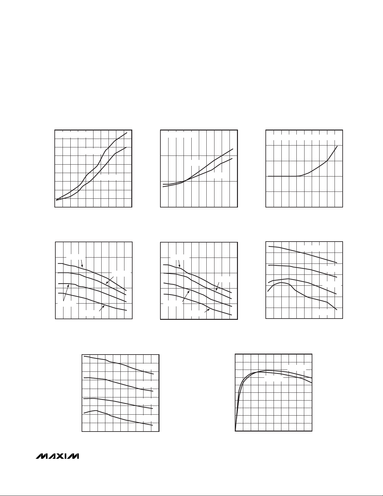
__________________________________________Typical Operating Characteristics
(Circuit of Figure 6, VIN= 5V ±10%, TA = +25°C, unless otherwise noted.)
OUTPUT RESISTANCE vs. TEMPERATURE
(FS = LOW)
10.5
MEASURED AT TP1
10.0
9.5
9.0
8.5
8.0
7.5
OUTPUT RESISTANCE (Ω)
7.0
6.5
6.0
-40 0 8040 120
-60 -20 60 140
VIN = 4.5V
VIN = 5.0V
20 100
TEMPERATURE (°C)
D1, D2 FREQUENCY vs. TEMPERATURE
(FS = LOW)
260
240
220
200
FREQUENCY (kHz)
180
160
VIN = 6.0V
VIN = 5.0V
VIN = 4.5V
-40 0 8040 120
-60 -20 60 140
20 100
TEMPERATURE (°C)
VIN = 5.5V
plot01
OUTPUT RESISTANCE (Ω)
plot04
FREQUENCY (kHz)
OUTPUT RESISTANCE vs. TEMPERATURE
(FS = HIGH)
15
MEASURED AT TP1
12
VIN = 4.5V
VIN = 5.0V
9
6
-40 0 8040 120
-60 -20 60 140
20 100
TEMPERATURE (°C)
D1, D2 FREQUENCY vs. TEMPERATURE
(FS = HIGH)
480
440
400
360
320
280
VIN = 6.0V
VIN = 5.5V
VIN = 5.0V
VIN = 4.5V
-40 0 8040 120
-60 -20 60 140
20 100
TEMPERATURE (°C)
plot02
SHUTDOWN CURRENT (μA)
plot05
SUPPLY CURRENT (μA)
SHUTDOWN SUPPLY CURRENT
vs. TEMPERATURE
1.0
INCLUDES SWITCH LEAKAGE CURRENTS
0.8
0.6
0.4
0.2
0
-40 0 8040 120
-60 -20 60 140
20 100
TEMPERATURE (°C)
SUPPLY CURRENT vs. TEMPERATURE
(FS = LOW)
600
550
500
450
400
350
300
250
-40 0 8040 120
-60 -20 60 140
VIN = 6.0V
VIN = 5.5V
VIN = 5.0V
VIN = 4.5V
20 100
TEMPERATURE (°C)
plot03
plot06
SUPPLY CURRENT vs. TEMPERATURE
(FS = HIGH)
850
800
750
700
650
600
550
SUPPLY CURRENT (μA)
500
450
400
-40 0 8040 120
-60 -20 60 140
20 100
TEMPERATURE (°C)
VIN = 6.0V
VIN = 5.5V
VIN = 5.0V
VIN = 4.5V
plot07
EFFICIENCY (%)
EFFICIENCY vs. LOAD CURRENT
(FS = LOW)
100
90
80
70
60
50
40
30
20
10
0
0 40 120 200
20 60 140100 180
VIN = 4.5V
80 160
LOAD CURRENT (mA)
VIN = 5.5V
plot08
Page 4
MAX253
Transformer Driver for
Isolated RS-485 Interface
4 _______________________________________________________________________________________
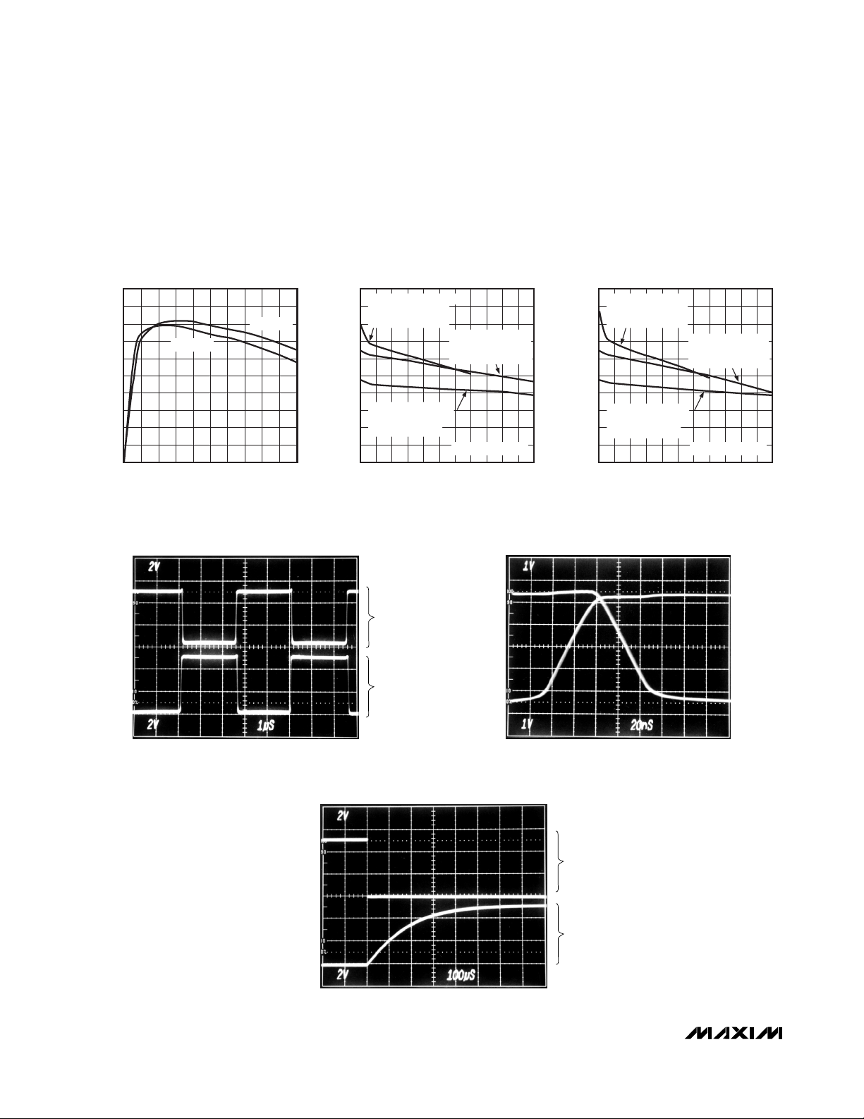
____________________________Typical Operating Characteristics (continued)
(Circuit of Figure 6, VIN= 5V ±10%, TA = +25°C, unless otherwise noted.)
EFFICIENCY vs. LOAD CURRENT
100
90
80
70
60
50
40
EFFICIENCY (%)
30
20
10
0
0 40 120 200
20 60 140100 180
(FS = HIGH)
VIN = 5.5V
VIN = 4.5V
80 160
LOAD CURRENT (mA)
SWITCHING WAVEFORMS
(TWO CYCLES)
10
plot09
9
8
7
6
5
4
OUTPUT VOLTAGE (V)
3
2
1
0
OUTPUT VOLTAGE vs. LOAD CURRENT
(FS = LOW)
CIRCUIT OF FIGURE 7
V
= 3.3V
IN
TURNS RATIO = 1:2.1
CIRCUIT OF FIGURE 6
= 5.0V
V
IN
TURNS RATIO = 1:1.3
CIRCUIT OF FIGURE 6
= 5.0V
V
IN
TURNS RATIO = 1:1
MEASURED AT TP1
80
20 60 140
0 40 220
D1
12 0100 160 180 200
LOAD CURRENT (mA)
OUTPUT VOLTAGE vs. LOAD CURRENT
10
plot10
CIRCUIT OF FIGURE 7
9
V
= 3.3V
IN
TURNS RATIO = 1:2.1
8
7
6
5
4
OUTPUT VOLTAGE (V)
CIRCUIT OF FIGURE 6
3
V
= 5.0V
IN
2
TURNS RATIO = 1:1
1
0
20 60 140
0 40 220
SWITCHING WAVEFORMS
(BREAK BEFORE MAKE)
(FS = HIGH)
CIRCUIT OF FIGURE 6
= 5.0V
V
IN
TURNS RATIO = 1:1.3
MEASURED AT TP1
80
12 0100 160 180 200
LOAD CURRENT (mA)
plot11
D1
D2
CIRCUIT OF FIGURE 1
CIRCUIT OF FIGURE 1
TIME FROM SHUTDOWN TO POWER-UP
SD
TP1 (OUTPUT VOLTAGE)
CIRCUIT OF FIGURE 6
D2
Page 5
MAX253
Transformer Driver for
Isolated RS-485 Interface
_______________________________________________________________________________________ 5
__________________Pin Configuration _____________________Pin Description
Not internally connected.N.C.5
5V supply voltage.V
CC
6
GND27
Open drain of N-channel transformer drive 2.D28
SD4
FS3
PIN
GND12
Open drain of N-channel transformer drive 1.D11
FUNCTIONNAME
Ground. Connect both GND1 and GND2
to ground.
Frequency switch. If FS = VCCor open,
switch frequency = 350kHz; if V
FS
= 0V,
switch frequency = 200kHz.
Shutdown. Ground for normal operation,
connect high for shutdown.
Ground. Connect both GND1 and GND2
to ground.
TOP VIEW
GND1
D1
1
2
FS
3
SD
4
DIP/SO/μMAX
+
MAX253
8
D2
GND2
7
V
6
CC
5
N.C.
Page 6
MAX253
Transformer Driver for
Isolated RS-485 Interface
6 _______________________________________________________________________________________
_______________Detailed Description
The MAX253 is an isolated power-supply transformer
driver specifically designed to form the heart of a fully
isolated RS-485 data interface. Completely isolated
communications are obtained by combining the
MAX253 with a linear regulator, a center-tapped transformer, optocouplers, and the appropriate Maxim interface product (as described in the
Isolated RS-485/RS-
232 Data Interface
section).
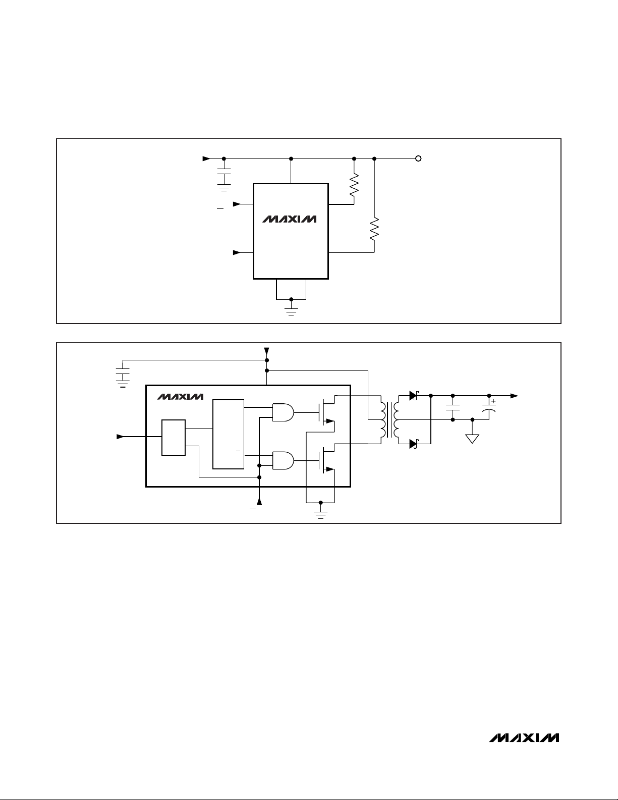
The MAX253 consists of an RC oscillator followed by a
toggle flip-flop, which generates two 50% duty-cycle
square waves, out-of-phase at half the oscillator fre-
quency (Figure 2). These two signals drive the groundreferenced output switches. Internal delays ensure
break-before-make action between the two switches.
Ground SD for normal operation. When high, SD disables all internal circuitry, including the oscillator and
both power switches.
Pulling FS low reduces the oscillator frequency and lowers the supply current (see Supply Current vs.
Temperature in the
Typical Operating Characteristics
).
FS includes a weak pull-up, so it will be set to the highfrequency state if not connected.
MAX253
D1
D2FS
GND1 GND2
V
CC
1
8
4
6
27
3
SD
FREQUENCY
SWITCH
ON / OFF
R2
50Ω
R1
50Ω
V
IN
5V
C1
0.1µF
Figure 1. Test Circuit
MAX253
D1
D2
FS
GND2 GND1
V
CC
FREQUENCY
SWITCH
C3
C1
C2
5V @ 200mA
ISO OUTPUT
5V
N
N
Q
Q
OSC
F / F
V
IN
SD
ON / OFF
400kHz/
700kHz
T
ISO
GND
Figure 2. Block Diagram
Page 7

MAX253
Transformer Driver for
Isolated RS-485 Interface
_______________________________________________________________________________________ 7
Figure 3. Typical RS-485 Application Circuit, 5V Configuration
V
IN
5V
ON / OFF
DI
DE
RO
C1
0.1μF
4
*74HC04
*74HC04
*74HC04
6
V
CC
MAX253
SD
GND1 GND2
27
390Ω
390Ω
3.3kΩ
ISOLATION
BARRIER
PC410 / 417
3
PC357T
1N5817
1N5817
4
6
5
4
0.1μF
82
C3
3.3kΩ
IN OUT
C2
22μF
3.3kΩ
MAX667
4
SHDNSET GND
564
8
V
DI
CC
ISO 5V
C4
22μF
6
A
1
D1
8
D2
3
FS
1CT:1.3CT**
1
1
MAX481
6
5
2
PC410 / 417
3
3
1
390Ω
1
MAX483
DE
MAX485
MAX487
RO
RE GND
485
I/O
7
B
52
*74HC04 OR EQUIVALENT
4
** SEE TABLE 2
3
Page 8

MAX253
Transformer Driver for
Isolated RS-485 Interface
8 _______________________________________________________________________________________
Figure 4. Typical RS-485 Application Circuit, 3.3V Configuration
V
IN
3.3V
ON / OFF
DI
DE
RO
C1
0.1µF
5
4
6
*74HC04
*74HC04
*74HC04
N.C.
MAX253
SD
V
CC
GND1 GND2
27
390Ω
390Ω
3.3kΩ
D1
D2
FS
1
8
3
1N5817
C5
0.1µF
1
1
6
5
ISOLATION
BARRIER
1CT:2.1CT**
1N5817
PC410 / 417
3
PC357T
2
PC410 / 417
1N5817
1N5817
4
3
82
C3
0.1µF
6
5
4
3.3kΩ
IN OUT
C2
22µF
3.3kΩ
MAX667
4
SHDNSET GND
564
8
V
DI
CC
ISO 5V
C4
22µF
6
A
MAX481
3
MAX483
DE
MAX485
485
I/O
MAX487
7
1
390Ω
1
RO
RE GND
B
52
*74HC04 OR EQUIVALENT
4
3
** SEE TABLE 2
Page 9

MAX253
Transformer Driver for
Isolated RS-485 Interface
_______________________________________________________________________________________ 9
Figure 5. Typical RS-232 Application Circuit
V
IN
5V
ON / OFF
C1
0.1µF
5
N.C.
4
SD
GND1 GND2
27
6
V
CC
MAX253
1
D1
8
D2
3
FS
ISOLATION
BARRIER
1CT:1.3CT**
1N5817
1N5817
0.1µF
82
C3
C2
22µF
IN OUT
MAX667
5 x 3.3kΩ
10 x PC417
T1
IN
T2
IN
T3
IN
T4
IN
T5
IN
*74HC04
74HC04
74HC04
74HC04
74HC04
390Ω
390Ω
390Ω
390Ω
390Ω
1
2
6
5
83
T1
4
74
T2
15 2
T3
16 1
T4
22 19
T5
5 X 3.3kΩ
R1
R2
R3
R4
R5
74HC04
OUT
74HC04
OUT
74HC04
OUT
74HC04
OUT
74HC04
OUT
6
5
1
24
390Ω
390Ω
390Ω
390Ω
390Ω
910
R1
65
R2
23 24
R3
17 18
R4
14 13
R5
*74HC04 OR EQUIVALENT
** SEE TABLE 2
4N25 LOWER SPEED, LOWER COST ALTERNATE OPTOCOUPLER CONFIGURATIONS (FOR DATA RATES BELOW 9.6kbps)
4N25
6
T
IN
*74HC04
390Ω
1N5711
1
2
3.3kΩ
5
ISO
4
GND
V
ISO
T
CC
R
OUT
IN
74HCO4
3.3kΩ
1N5711
5
4N25
6
4
SHDNSET GND
V
CC
IN
IN
IN
IN
IN
MAX205
OUT
OUT
OUT
OUT
OUT
1
2
564
ISO
GND
GND
T1
T2
T3
T4
T5
ENSD
390Ω
ISO 5V
C4
22µF
OUT
OUT
OUT
OUT
OUT
R1
IN
R2
IN
R3
IN
R4
IN
R5
IN
2021
V
CC
ISO
R
OUT
Page 10

MAX253
Transformer Driver for
Isolated RS-485 Interface
10 ______________________________________________________________________________________
* PC-Series Optocouplers, Sharp Electronics
USA Phone: (206) 834-2500
FAX: (206) 834-8903
Sharp Electronics, Europe GmbH
Germany Phone: (040) 2376-0
FAX: (040) 230764
__________Applications Information
Figures 3–5 are typical isolated RS-485/RS-232 data-interface circuits. These circuits withstand 1800V
RMS
(1sec)
and are intended for industrial communications and control
applications where very high voltage transients, differential
ground potentials, or high noise may be encountered.
Table 2 lists transformer characteristics for the applications of Figures 3–10. Some suggested manufacturers
of transformers, transformer cores, and optocouplers
are listed in Table 3, along with their respective phone
and fax numbers.
Important layout considerations include:
♦♦
For maximum isolation, the “isolation barrier” should not
be breached. Connections and components from one
side should not be located near those of the other side.
♦♦
Since the optocoupler outputs are relatively highimpedance nodes, they should be located as close
as possible to the Maxim interface IC. This minimizes stray capacitance and maximizes data rate.
Refer to the µMAX package information for pin spacing
and physical dimensions.
Isolated RS-485 Data Interface
The MAX253 power-supply transformer driver is
designed specifically for isolated RS-485 data-interface
applications. The application circuits of Figures 3 and 4
combine the MAX253 with a low-dropout linear regulator,
a transformer, several high-speed optocouplers, and a
Maxim RS-485 interface device. With a few modifications to these circuits, full-duplex communications can
be implemented by substituting the MAX481/MAX485
with the MAX490/MAX491 (for data rates up to 2.5Mbps)
or substituting the MAX483/MAX487 with the
MAX488/MAX489 (for data rates up to 250kbps).
The data transfer rates of the application circuits in
Figures 3 and 4 are critically limited by the optocouplers. Table 1 lists suggested optocouplers and the
appropriate Maxim interface device for data-transfer
rates up to 2.5Mbps.
Refer to the MAX1480 data sheet for a complete isolated RS-485 solution in one package.
Isolated RS-232 Data Interface
The MAX253 is ideal for isolated RS-232 data-interface
applications requiring more than four transceivers. The
1W power output capability of the MAX253 enables it to
drive more than 10 transceivers simultaneously. Figure 5
shows the typical application circuit for a complete
120kbps isolated RS-232 data interface. The figure
also shows how the Sharp PC417 optocouplers can be
replaced by the lower-cost 4N25 devices to achieve
data-transfer rates up to 9.6kbps.
For 3.3V operation, substitute the primary portion of
Figure 5 with the circuit of Figure 7.
For applications requiring two transceivers or fewer,
refer to the MAX250/MAX251 or MAX252 data sheet.
Isolated Power Supplies
The MAX253 is a versatile isolated power driver, capable of driving a center-tapped transformer primary from
a 5V or a 3.3V DC power supply (Figures 6 and 7). The
secondary can be wound to provide any isolated voltage needed at power levels up to 1W with a 5V supply,
or 600mW with a 3.3V supply. Figure 6 shows a typical
5V to isolated 5V application circuit that delivers up to
200mA of isolated 5V power.
In Figure 7, the MAX253 is configured to operate from a
3.3V supply, deriving a “boost” VCCfor the MAX253 by
connecting diodes to both ends of the transformer primary. This produces nearly double the input supply,
and may be useful for other applications, as shown in
Figure 4. The average current in each MAX253 switch
must still be limited to less than 200mA, so the total
power available is approximately 600mW.
Table 1. Optocouplers and RS-485 Interface ICs for Various Data Rates
DATA RATE
FULL DUPLEX
RS-485 IC
HALF DUPLEX
RS-485 IC
OPTOCOUPLER
FOR DI / RO
OPTOCOUPLER
FOR DE
250kbps MAX488/MAX489 MAX483/MAX487 PC417* PC357T*
2.5Mbps MAX490/MAX491 MAX481/MAX485 PC410* PC357T
Page 11

MAX253
Transformer Driver for
Isolated RS-485 Interface
______________________________________________________________________________________ 11
V
Figure 6. 5V to Isolated 5V Application Circuit
C3
0.1µF
C1
0.1µF
C2
22µF
5V @ 100mA
ISO OUTPUT
3.3V
V
IN
L2
25µH
MAX253
D1
D2FS
GND1 GND2
V
CC
1
8
627
3
FREQUENCY
SWITCH
SD
4
C7
2.2µF
FILTER
OUTPUT
OUTPUT
OPTIONAL 21kHz LOWPASS OUTPUT FILTER
TP1
1N5817
1CT:2.1CT*
1N5817
ON / OFF
1N5817
1N5817
C4
0.1µF
*SEE TABLE 2
Figure 7. 3.3V to Isolated 5V Application Circuit
IN
5V
*SEE TABLE 2
C1
0.1µF
ON / OFF
FREQUENCY
SWITCH
4
3
V
SD
MAX253
GND1 GND2
27
6
CC
D1
D2FS
1CT:1.3CT*
1
8
1N5817
1N5817
C3
0.1µF
OPTIONAL 21kHz LOWPASS OUTPUT FILTER
L2
25µH
OUTPUT
TP1
C2
22µF
5V @ 200mA
ISO OUTPUT
FILTER
OUTPUT
C7
2.2µF
Page 12

MAX253
Transformer Driver for
Isolated RS-485 Interface
12 ______________________________________________________________________________________
Figure 8. Typical 4mA to 20mA Application Circuit
Output-Ripple Filtering
A simple lowpass pi-filter (Figures 6 and 7) can be added
to the output to reduce output ripple noise to approximately
10mVp-p. The cutoff frequency shown is 21kHz. Since the
filter inductor is in series with the circuit output, minimize its
resistance so the voltage drop across it is not excessive.
Isolated 4mA to 20mA Analog Interface
The 4mA to 20mA current loop is a standard analog
signal range that is widely used in the process-control
industry for transducer and actuator control signals.
These signals are commonly referred to a distant
ground that may be at a considerably higher voltage
with respect to the local ground.
An analog signal in the range of 0.1V to 0.5V is applied
to the first MAX480 to generate a signal current in the
range of 20µA to 100µA. This low-level signal is transferred across the barrier by the Siemens IL300 linear
optocoupler. This device is unique in that it corrects
the dominant nonlinearity present in most optocou-
plers—the LED efficiency variation. The IL300 is really
two optocouplers in the same package sharing the same
LED; one detector is across the isolation barrier, the
other is on the same side as the LED (Figure 8). The latter detector is used to generate a feedback signal identical to the signal on the isolated side of the barrier. The
current signal transferred across the barrier is converted
back to a voltage that matches the input in the 100mV to
500mV range. This voltage is then transformed to the
final 4mA to 20mA current signal range by the second
MAX480, Darlington stage, and the 20Ω resistor.
Isolated ADC
Almost any serial-interface device is a candidate for
operation across an isolation barrier; Figure 10 illustrates one example. The MAX176 analog-to-digital
converter (ADC) operates from 5V and -12V supplies,
provided by the multiple-tapped secondary and linear
regulators. If some additional isolated power is needed
for signal conditioning, multiplexing, or possibly for a
V
IN
5V
5V
0.1V to 0.5V
*SEE TABLE 2
4
3
2
SD
GND1 GND2
MAX480
6
V
CC
D1
MAX253
D2
27
7
6
4
49.9kΩ
ISOLATION
BARRIER
1
8
1CT:5CT*
1N5817
1N5817
1
2
3
4
IL300
24V UNREGULATED
6
5
10µF
49.9kΩ
3
2
MAX480
78L05
R
L
0kΩ to 1kΩ
ISO
5V
6
7
4
2N3904
2N3904
10kΩ
24.9Ω
Page 13

MAX253
Transformer Driver for
Isolated RS-485 Interface
______________________________________________________________________________________ 13
Figure 9a. Half-Wave Rectifier—Bipolar
V
OUT
≈ -V
IN
OUTPUT
V
IN
INPUT
MAX253
GND1 GND2
V
CC
1
8
6
27
1CT:1CT*
D1
D2
V
OUT
≈ +V
IN
OUTPUT
4 x 1N5817
*SEE TABLE 2
Figure 9b. Full-Wave Rectifier—Bipolar
V
IN
INPUT
MAX253
GND1 GND2
V
CC
1
8
6
27
1CT:1CT*
D1
D2
V
OUT
≈ 2 x V
IN
OUTPUT
4 x 1N5817
*SEE TABLE 2
Figure 9c. Full-Wave Rectifier—Unipolar
V
IN
INPUT
6
V
CC
1
D1
MAX253
8
GND1 GND2
27
*SEE TABLE 2
D2
1CT:1CT*
1N5817
1N5817
+V
OUT
≈ 2V
OUT
≅ R
-
L
≈ -2V
IN
IN
OUTPUT
+
R
L
+
R
L
-
R
L
-V
OUTPUT
Page 14

MAX253
Transformer Driver for
Isolated RS-485 Interface
14 ______________________________________________________________________________________
Figure 10. Typical Isolated ADC Application
ISO
5V
78L05
ISO
-12V
10μF
4 x 1N5817
79 L12
10μF
ISOLATION
BARRIER
1CT : 1.5CT : 3CT*
V
IN
5V
1
D1
6
8
MAX253
V
CC
D2
GND1 GND2
27
4
SD
ON/OFF
10μF
0.1μF
ANALOG
10μF
SIGNAL
GROUND
INPUT
0.1μF
5V
6N136
8
3kΩ
MAX176
1
V
DD
2
AIN
3
VREF
4
GND
V
CONVST
CLOCK
DATA
8
SS
7
6
5
0.1μF10μF
3kΩ
470Ω
7
6
5
6N136
8
7
6
5
6N136
1
2
3
4
1
200Ω
2
3
4
1
200Ω
2
3
4
8
7
6
5
74HC04
8.2kΩ
5V
5V
14
11
12
10
13 8
14
11
12
10
13 8
SER
74HC595
SCK
RCK
SCLR
QH′
SER
74HC595
SCK
RCK
SCLR
74HC04
8
QH
QG
QF
QE
QD
QC
QB
QA
QH
QG
QF
QE
QD
QC
QB
QA
INPUT CLOCK
7
6
5
4
3
D11(MSB)
2
D10
1
D9
15
D8
16
5V
0.1μF
7
D7
6
D6
5
D5
4
D4
3
D3
2
D2
1
D1
15
D0(LSB)
16
5V
0.1μF
START
*SEE TABLE 2
Page 15

MAX253
Transformer Driver for
Isolated RS-485 Interface
______________________________________________________________________________________ 15
sensor, an extra several hundred milliwatts could easily
be supplied by the circuit, as shown. A 12V supply
could be generated by adding two more diodes to the
ends of the secondary, and a -5V supply could be generated by connecting additional diodes to the 1/4 and
3/4 tap points on the secondary. For 5V only applications, the MAX187 is recommended.
______________Component Selection
Transformer Selection
The transformer primary used with the MAX253 must be
a center-tapped winding with sufficient ET product to
prevent saturation at the worst-case lowest selected
frequency. The MAX253’s guaranteed minimum frequency with the FS pin held low is 150kHz, equating to
a maximum period of 6.67µs. The required ET product
for half the primary is simply the product of the maximum supply voltage and half the maximum period.
With FS connected high, the guaranteed minimum frequency is 250kHz, giving a maximum period of 4µs.
The secondary winding may or may not be center
tapped, depending on the rectifier topology used. The
phasing of the secondary winding is not critical. In
some applications, multiple secondaries might be
required. Half-wave rectification could be used, but is
discouraged because it normally adds a DC imbalance
to the magnetic flux in the core, reducing the ET product. If the DC load is imbalanced, full-wave rectification
is recommended, as shown in Figure 9b.
The transformer turns ratio must be set to provide the
minimum required output voltage at the maximum
anticipated load with the minimum expected input volt-
Table 2. Typical Transformer Characteristics
Table 3. Transformer, Transformer Core, and Optocoupler Suppliers
CHARACTERISTIC 5V to ±10V 5V to 5V 3.3V to 5V 5V to 24V 5V to ±5V; ±12V
Figure 9a 2, 3, 5, 6 4, 7 8 10
Turns Ratio 1CT*:1 1CT:1.3CT 1CT:2.1CT 1CT:5CT 1CT:1.5CT:3CT
Primary 44CT 44CT 28CT 44CT 44CT
Typical
Windings
Secondary 44 56CT 56CT 220CT 66CT, 132CT
FS Low 18.3V-µs 18.3V-µs 12V-µs 18.3V-µs 18.3V-µs
Primary ET
Product
FS High 11V-µs 11V-µs 7.2V-µs 11V-µs 11V-µs
TRANSFORMERS TRANSFORMER CORES OPTOCOUPLERS
BH Electronics
Phone: (507) 532-3211
FAX: (507) 532-3705
Philips Components
Phone: (407) 881-3200
FAX: (407) 881-3300
Quality Technology
Phone: (408) 720-1440
FAX: (408) 720-0848
Coilcraft
Phone: (708) 639-6400
FAX: (708) 639-1469
Magnetics Inc.
Phone: (412) 282-8282
FAX: (412) 282-6955
Sharp Electronics
Phone: (206) 834-2500
FAX: (206) 834-8903
Coiltronics
Phone: (516) 241-7876
FAX: (516) 241-9339
Fair-Rite Products
Phone: (914) 895-2055
FAX: (914) 895-2629
Siemens Components
Phone: (408) 777-4500
FAX: (408) 777-4983
*CT = Center Tapped
Page 16

MAX253
Transformer Driver for
Isolated RS-485 Interface
16 ______________________________________________________________________________________
age. In addition, include in the calculations an
allowance for worst-case losses in the rectifiers. Since
the turns ratio determined in this manner will ordinarily
produce a much higher voltage at the secondary under
conditions of high input voltage and/or light loading, be
careful to prevent an overvoltage condition from occurring (see Output Voltage vs. Load Current in the
Typical
Operating Characteristics
).
Transformers used with the MAX253 will ordinarily be
wound on high-permeability magnetic material. To minimize radiated noise, use common closed-magneticpath physical shapes (e.g., pot cores, toroids, E/I/U
cores). A typical core is the Philips 213CT050-3B7,
which is a toroid 0.190” in diameter and 0.05” thick.
For operation with this core at 5.5V maximum supply
voltage, the primary should have approximately 22
turns on each side of the center tap, or 44 turns total.
This will result in a nominal primary inductance of
approximately 832µH. The secondary can be scaled to
produce the required DC output.
Diode Selection
The MAX253’s high switching frequency demands
high-speed rectifiers. Schottky diodes are recommended. Ensure that the Schottky diode average current rating exceeds the load-current level. The 1N5817
is a good choice for through-hole applications, and the
NIEC* SB05W05C dual in an SOT-23 package is recommended for surface-mount applications. Use the
higher frequency setting to reduce ripple.
Output Filter Capacitor
In applications sensitive to output-ripple noise, the output filter capacitor C2 should have a low effective
series resistance (ESR), and its capacitance should
remain fairly constant over temperature. Sprague 595D
surface-mount solid tantalum capacitors and Sanyo
OS-CON through-hole capacitors are recommended
due to their extremely low ESR. Capacitor ESR usually
rises at low temperatures, but OS-CON capacitors provide very low ESR below 0°C.
In applications where output ripple is not critical, a
0.1µF chip or ceramic capacitor is sufficient. Refer to
Table 4 for suggested capacitor suppliers. Use the
higher frequency setting to reduce ripple.
Input Bypass Capacitor
The input bypass capacitor C1 is not critical. Unlike
switching regulators, the MAX253’s supply current is
fairly constant, and is therefore less dependent on the
input bypass capacitor. A low-cost 0.1µF chip or
ceramic capacitor is normally sufficient for input
bypassing.
* Nihon Inter Electronics Corp.
USA Phone: (805) 867-2555
FAX: (805) 867-2556
Japan Phone: 81-3-3494-7411
FAX: 81-3-3494-7414
Table 4. Suggested Capacitor Suppliers
PRODUCTION METHOD CAPACITORS
Surface Mount
Matsuo
267 series (low ESR)
USA Phone: (714) 969-2491, FAX: (714) 960-6492
Sprague Electric Co.
595D/293D series (very low ESR)
USA Phone: (603) 224-1961, FAX: (603) 224-1430
Murata Erie
Ceramic
USA Phone: (800) 831-9172, FAX: (404) 436-3030
High-Performance
Through Hole
Sanyo
OS-CON series (very low ESR)
USA Phone: (619) 661-6835, FAX: (619) 661-1055
Japan Phone: 81-7-2070-1005, FAX: 81-7-2070-1174
Through Hole
Nichicon
PL series (low ESR)
USA Phone: (708) 843-7500, FAX: (708) 843-2798
Japan Phone: 81-7-5231-8461, FAX: 81-7-5256-4158
Page 17

MAX253
Transformer Driver for
Isolated RS-485 Interface
______________________________________________________________________________________ 17
___________________Chip Information
PROCESS: CMOS
PACKAGE TYPE PACKAGE CODE DOCUMENT NO.
8 µMAX U8+1
21-0036
8 PDIP P8+1
21-0043
8 SO S8+4
21-0041
8 CDIP J8-2
21-0045
Package Information
For the latest package outline information and land patterns,
go to www.maxim-ic.com/packages
. Note that a “+”, “#”, or
“-” in the package code indicates RoHS status only. Package
drawings may show a different suffix character, but the drawing
pertains to the package regardless of RoHS status.
Page 18

Revision History
Maxim cannot assume responsibility for use of any circuitry other than circuitry entirely embodied in a Maxim product. No circuit patent licenses are
implied. Maxim reserves the right to change the circuitry and specifications without notice at any time.
18
____________________Maxim Integrated Products, 120 San Gabriel Drive, Sunnyvale, CA 94086 408-737-7600
© 2010 Maxim Integrated Products Maxim is a registered trademark of Maxim Integrated Products, Inc.
Transformer Driver for
Isolated RS-485 Interface
MAX253
REVISION
NUMBER
0 1/94 Init ial release —
1 8/09 Deleted the MAX253EUA part number from the Ordering Information table 1
REVISION
DATE
DESCRIPTION
PAGES
CHANGED
2 4/10 Added automoti ve qualified part number to the Ordering Information table 1
 Loading...