

For free samples & the latest literature: http://www.maxim-ic.com, or phone 1-800-998-8800.
For small orders, phone 408-737-7600 ext. 3468.
_______________General Description
The MAX2511 is a complete, highly integrated IF transceiver for applications employing a dual-conversion
architecture. Alternatively, the MAX2511 can be used
as a single-conversion transceiver if the RF operating
frequency ranges from 200MHz to 440MHz.
In a typical application, the receiver downconverts a
high IF/RF (200MHz to 440MHz) to a 10.7MHz low IF
using an image-reject mixer. Functions include an
image-reject downconverter with 34dB of image suppression followed by an IF buffer that can drive an offchip IF filter; an on-chip limiting amplifier offering 90dB
of monotonic received-signal-strength indication (RSSI);
and a robust limiter output driver. The transmit imagereject mixer generates a clean output spectrum to minimize filter requirements. It is followed by a 40dB
variable-gain amplifier that maintains IM3 levels below
-35dBc. Maximum output power is 2dBm. A VCO and
oscillator buffer for driving an external prescaler are
also included.
The MAX2511 operates from a 2.7V to 5.5V supply and
includes flexible power-management control. Supply
current is reduced to 0.1µA in shutdown mode.
For applications using in-phase (I) and quadrature (Q)
baseband architecture for the transmitter, Maxim offers
a corresponding transceiver product: the MAX2510.
The MAX2510 has features similar to those of the
MAX2511, but upconverts I/Q baseband signals using
a quadrature upconverter.
________________________Applications
PWT1900 Wireless Handsets and
Base Stations
PACS, PHS, DECT and Other PCS
Wireless Handsets and Base Stations
400MHz ISM Transceivers
IF Transceivers
Wireless Data Links
____________________________Features
♦ Single +2.7V to +5.5V Supply
♦ Complete Receive Path:
200MHz to 440MHz (first IF) to
8MHz to 13MHz (second IF)
♦ Limiter with Differential Outputs (adjustable level)
♦ RSSI Function with 90dB Monotonic Dynamic
Range
♦ Complete Transmit Path:
8MHz to 13MHz (second IF) to
200MHz to 440MHz (first IF)
♦ On-Chip Oscillator with Voltage Regulator
and Buffer
♦ Advanced System Power Management
(four modes)
♦ 0.1µA Shutdown Supply Current
MAX2511
Low-Voltage IF Transceiver
with Limiter and RSSI
________________________________________________________________
Maxim Integrated Products
1
28
27
26
25
24
23
21
20
19
18
17
16
15
1LIMIN VREF
MIXOUT
GND
RXIN
TXOUT
TXOUT
V
CC
V
CC
GND
TXEN
RXEN
TXIN
TXIN
CZ
CZ
RSSI
GC
TANK
TANK
GND
OSCOUT
LIMOUT
LIMOUT
V
CC
V
CC
2
3
4
5
6
8
9
10
11
12
13
14
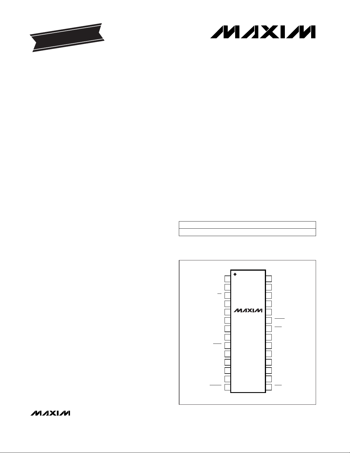
QSOP
TOP VIEW
MAX2511
22 RXINGND 7
__________________Pin Configuration
PART
MAX2511EEI -40°C to +85°C
TEMP. RANGE PIN-PACKAGE
28 QSOP
EVALUATION KIT
AVAILABLE
______________Ordering Information
Typical Operating Circuit appears at end of data sheet.
19-1209; Rev 0; 10/97
MAX2511
Low-Voltage IF Transceiver
with Limiter and RSSI
2 _______________________________________________________________________________________
ABSOLUTE MAXIMUM RATINGS
DC ELECTRICAL CHARACTERISTICS
(VCC= +2.7V to +5.5V, 0.01µF across CZ and CZ; TANK = TANK; MIXOUT tied to VREF through a 165Ω resistor; GC open, RXIN =
RXIN; TXOUT = TXOUT = V
CC
; TA= -40°C to +85°C, unless otherwise noted. Typical values are at TA= +25°C.)
Stresses beyond those listed under “Absolute Maximum Ratings” may cause permanent damage to the device. These are stress ratings only, and functional
operation of the device at these or any other conditions beyond those indicated in the operational sections of the specifications is not implied. Exposure to
absolute maximum rating conditions for extended periods may affect device reliability.
VCCto GND .............................................................-0.3V to 8.0V
V
CC
to Any Other VCC........................................................±0.3V
TXIN, TXIN Input Voltage............................-0.3V to (V
CC
+ 0.3V)
TXIN to TXIN Differential Voltage....................................±300mV
RXIN, RXIN Input Voltage........................................-0.3V to 1.6V
TANK, TANK Voltage...............................................-0.3V to 2.0V
LIMIN Voltage .............................(VREF - 1.3V) to (VREF + 1.3V)
LIMOUT, LIMOUT Voltage ..............(V
CC
- 1.6V) to (VCC+ 0.3V)
RXEN, TXEN, GC Voltage...........................-0.3V to (V
CC
+ 0.3V)
RXEN, TXEN, GC Input Current............................................1mA
RSSI Voltage...............................................-0.3V to (VCC+ 0.3V)
Continuous Power Dissipation (T
A
= +70°C)
QSOP (derate 11mW/°C above 70°C) ...........................909mW
Operating Temperature Range
MAX2511EEI......................................................-40°C to +85°C
Junction Temperature......................................................+150°C
Storage Temperature Range.............................-65°C to +165°C
Lead Temperature (soldering, 10sec).............................+300°C
Internally terminated to 1.35VGC Input Resistance 60 80 125
kΩ
LIMOUT, LIMOUT
Differential Output Impedance
2
kΩ
(Note 1)
RXEN, TXEN
RXEN, TXEN
CONDITIONSPARAMETER MIN TYP MAX UNITS
Digital Input Current Low -5 -1 µA
Digital Input Current High 23 32 µA
VREF Voltage
V
CC
/ 2 - V
CC
/ 2 V
CC
/ 2 +
100mV 100mV
V
Digital Input Voltage High
Operating Voltage Range 2.7 3.0 5.5 V
2.0 V
Digital Input Voltage Low 0.4 V
24
26
9.5
VCC= 3.0V
TA= +25°C
Typical Supply Current
0.1
mA
38.5
45
14.5
VCC= 2.7V to 5.5V,
TA= -40°C to +85°C
Worst-Case Supply Current
5
mA
µA
µA
Rx mode, RXEN = high,
TXEN = low
Tx mode, RXEN = low,
TXEN = high, VGC= 0.5V
Standby mode, RXEN = high,
TXEN = high
Shutdown mode, RXEN = low,
TXEN = low
Rx mode, RXEN = high,
TXEN = low
Tx mode, RXEN = low,
TXEN = high, VGC= 0.5V
Standby mode, RXEN = high,
TXEN = high
Shutdown mode, RXEN = low,
TXEN = low
MAX2511
Low-Voltage IF Transceiver
with Limiter and RSSI
_______________________________________________________________________________________ 3
AC ELECTRICAL CHARACTERISTICS
(MAX2511 test fixture, VCC= +3.0V, RXEN = TXEN = low, 0.01µF across CZ and CZ, MIXOUT tied to VREF through 165Ω resistor,
TXIN, TXIN tied to VREF through 50Ω resistor, TXOUT and TXOUT loaded with 100Ω differential, GC open, LIMOUT, LIMOUT loaded
with 2kΩ differential, TANK and TANK driven with -2.5dBm from a 100Ω source; OSCOUT AC-terminated with 50Ω, 330pF at RSSI
pin, 0.1µF at VREF pin, Rx inputs and Tx outputs differentially coupled, P
RXIN, RXIN
= -28dBm (200Ω system), f
RXIN, RXIN
= 425MHz,
f
LO
= 435.7MHz, f
TXIN, TXIN
= 10.7MHz, TA= +25°C, unless otherwise noted.)
21.5 23.6 25.5
dBm-16
Downconverter Mixer Input 1dB
Compression Level
dBm-11Input Third-Order Intercept
dB25 34Image Rejection
UNITSMIN TYP MAXPARAMETER CONDITIONS
TA= +25°C
(Note 2)
Two tones at 424MHz and 425MHz,
-30dBm per tone
f
IMAGE
= fLO+ fIF= 446.4MHz
Vp-p2MIXOUT Maximum Voltage Swing
µs5Power-Up Time Standby to RX or TX (Note 3)
mVp-p
120 160
Limiter Output Level
VGC= 0.8V (Note 4)
475 625
950 1100
degrees3.6Phase Variation
-75dBm to 5dBm from 50Ω
dB80Minimum Linear RSSI Range
-75dBm to 5dBm from 50Ω
dB90Minimum Monotonic RSSI Range
-80dBm to 10dBm from 50Ω
mV/dB10.6RSSI Slope
-75dBm to 5dBm from 50Ω
dBm-82 -75RSSI Maximum Intercept (Note 5)
µs6.4RSSI Rise Time
Rise time to within 1dB accuracy; using a 100pF
capacitor from RSSI to GND
mV50 90 135Minimum-Scale RSSI Voltage At LIMIN input of -75dBm
mV850 940 1025Maximum-Scale RSSI Voltage At LIMIN input of 5dBm
dBm-65LO Leakage At RXIN port
-12 -9TA= +25°C (Note 8)
µs220Maximum Power-Up Time Shutdown to standby mode (Note 9)
dBc/Hz-88Phase Noise
MHz200 440Frequency Range
kHz±36Maximum LO Frequency Pulling
(Note 7)
At 10kHz offset
Standby mode to TX or RX mode
±1 ±2TA= +25°C
dB14Downconverter Mixer Noise Figure
dB
20 27
Downconverter Mixer Voltage Gain
TA= -40°C to +85°C (Note 1)
dB
±2.5
RSSI Relative Error
TA= -40°C to +85°C (Note 1)
dBm
-13
Oscillator Buffer Output Power
TA= -40°C to +85°C (Notes 1 and 8)
VGC= 2.0V (P
LIMIN
= +5dBm)
VGC= open
DOWNCONVERTER (RXEN = high)
LIMITING AMPLIFIER AND RSSI (RXEN = high)
OSCILLATOR (TXEN = RXEN = high)
MAX2511
Low-Voltage IF Transceiver
with Limiter and RSSI
4 _______________________________________________________________________________________
Note 1: Guaranteed by design and characterization.
Note 2: Driving RXIN or RXIN with a power level greater than the 1dB compression level forces the input stage out of its linear
range, causing harmonic and intermodulation distortion. The RSSI output increases monotonically with increasing input
levels beyond the mixer’s 1dB compression level.
Note 3: Assuming the supply voltage has been applied, this includes settling of the limiter offset correction and the Rx or Tx bias
stabilization time. Guaranteed by design.
Note 4: LIMOUT, LIMOUT loaded with 2kΩ differential. With no load, the output swing is approximately twice as large.
Note 5: The RSSI maximum intercept is the maximum input power (over a statistical sample of parts) at which the RSSI output is 0V.
This point is extrapolated from the linear portion of the RSSI voltage versus limiter input power. This specification and the
RSSI slope define the ideal behavior of the RSSI function (the slope and intercept of a straight line), while the RSSI relative
error specification defines the deviations from this line. See the RSSI Output Voltage vs. Limiter Input Power graph in the
Typical Operating Characteristics
.
Note 6: The RSSI relative error is the deviation from the best-fitting straight line of RSSI output voltage versus limiter input power.
A 0dB relative error is exactly on this line. The limiter input power range for this test is -75dBm to +5dBm from 50Ω. See the
RSSI Relative Error graph in the
Typical Operating Characteristics
.
Note 7: Operation outside this frequency range is possible but has not been characterized. At lower frequencies, it might be
necessary to overdrive the oscillator with an external signal source.
Note 8: If a larger output level is required, a higher value of load resistance (up to 100Ω) may be used.
Note 9: This assumes that the supply voltage has been applied, and includes the settling time of V
REF
, using the
Typical
Operating Circuit.
Note 10: Using two tones at 10.7MHz and 10.8MHz, 50mVp-p per tone at TXIN, TXIN. See
Typical Operating Characteristics
.
-44
Output Power
VGC= 0.5V, TA= +25°C
dBm
-19VGC= open, TA= +25°C
-5 -2VGC= 2.0V, TA= +25°C
-6VGC= 2.0V, TA= -40°C to +85°C (Note 1)
dBc40 30LO Rejection
dBm2Output 1dB Compression Point VGC= 2.0V
UNITSMIN TYP MAXPARAMETER CONDITIONS
AC ELECTRICAL CHARACTERISTICS (continued)
(MAX2511 test fixture, VCC= +3.0V, RXEN = TXEN = low, 0.01µF across CZ and CZ, MIXOUT tied to VREF through 165Ω resistor,
TXIN, TXIN tied to VREF through 50Ω resistor, TXOUT and TXOUT loaded with 100Ω differential, GC open, LIMOUT, LIMOUT loaded
with 2kΩ differential, TANK and TANK driven with -2.5dBm from a 100Ω source; OSCOUT AC-terminated with 50Ω, 330pF at RSSI
pin, 0.1µF at VREF pin, Rx inputs and Tx outputs differentially coupled, P
RXIN, RXIN
= -28dBm (200Ω system), f
RXIN, RXIN
= 425MHz,
f
LO
= 435.7MHz, f
TXIN, TXIN
= 10.7MHz, TA= +25°C, unless otherwise noted.)
-40
Output IM3 Level
0.5V < VGC< 1.87V
-40dBm < P
OUT
< -10dBm (Note 10)
dBc
-35VGC= 2.0V
dBc34 25Image Rejection
TRANSMITTER (TXEN = high, V
TXIN
and V
TXIN
= 100mVp-p differential)
MAX2511
Low-Voltage IF Transceiver
with Limiter and RSSI
_______________________________________________________________________________________
5
40
35
Tx MODE
Rx MODE
STANDBY MODE
0
-40 85
SUPPLY CURRENT
vs. TEMPERATURE
10
5
30
25
MAX2511 TOC01
TEMPERATURE (°C)
I
CC
(mA)
25
20
15
40
35
0
2.7 3.0 5.5
SUPPLY CURRENT
vs. SUPPLY VOLTAGE
10
5
30
25
MAX2511 TOC02
VCC (V)
I
CC
(mA)
4.0 4.5 5.03.5
20
15
STANDBY MODE
Tx MODE
Rx MODE
50
45
20
0 0.4
SUPPLY CURRENT
vs. GC VOLTAGE
40
30
35
MAX2511 TOC03
GC VOLTAGE (V)
I
CC
(mA)
1.6 2.0 2.4 2.8 3.21.20.8
25
Tx MODE
Rx MODE
2.5
0
2.7 3.0 5.5
SHUTDOWN CURRENT
vs. SUPPLY VOLTAGE
0.5
2.0
1.5
MAX2511 TOC04
SUPPLY VOLTAGE (V)
I
CC
(µA)
4.0 4.5 5.03.5
1.0
TA = +85°C
TA = +25°C
TA = -40°C
25
24
23
21
20
22
19
MAX2511-TOC05
VCC (V)
2.7 3.0 3.5 4.0 4.5 5.0 5.5
DOWNCONVERTER MIXER CONVERSION
GAIN vs. SUPPLY VOLTAGE
GAIN (dB)
RXEN = HIGH
TXEN = LOW
TA = +85°C
TA = +25°C
TA = -40°C
22.0
23.0
22.5
23.5
24.5
24.0
RXEN = HIGH
TXEN = LOW
25.0
200 275 350 425
DOWNCONVERTER GAIN
vs. RXIN FREQUENCY
MAX2511/TOC07A
RXIN FREQUENCY (MHz)
VOLTAGE GAIN (dB)
__________________________________________Typical Operating Characteristics
(MAX2511 test fixture, VCC= +3.0V, 0.01µF across CZ and CZ, MIXOUT tied to VREF through 165Ω resistor, TXIN, TXIN tied to VREF
through 50Ω resistor, TXOUT and TXOUT loaded with 100Ω differential, GC open, LIMOUT, LIMOUT loaded with 2kΩ differential,
TANK and TANK driven with -2.5dBm from a 100Ω source; OSCOUT AC-terminated with 50Ω, 100pF at RSSI pin, 0.1µF at VREF pin,
Rx inputs and Tx outputs differentially coupled, P
RXIN, RXIN
= -28dBm (200Ω system), f
RXIN, RXIN
= 425MHz, f
LO
= 435.7MHz, f
TXIN,
TXIN
= 10.7MHz, TA= +25°C, unless otherwise noted.)

MAX2511
Low-Voltage IF Transceiver
with Limiter and RSSI
6 _______________________________________________________________________________________
70
60
50
30
20
40
0
10
MAX2511-TOC09
VCC (V)
DOWNCONVERTER INPUT 1dB
COMPRESSION LEVEL
1dB COMPRESSION LEVEL (mVrms)
TXEN = LOW
RXEN = HIGH
TA = +85°C
TA = +25°C
TA = -40°C
2.7 3.0 3.5 4.0 4.5 5.0 5.5
-250
0
-100
100
-200
50
-50
-150
RX OFF REAL
150
200
250
200 300 400 500
RXIN DIFFERENTIAL INPUT IMPEDANCE
vs. FREQUENCY
MAX2511/TOC10
FREQUENCY (MHz)
REAL AND IMAGINARY IMPEDANCE (Ω)
RX OFF IMAGINARY
RX MODE REAL
RX MODE IMAGINARY
1.2
0
0 0.4
LIMITER OUTPUT LEVEL
vs. GC VOLTAGE
1.0
MAX2511-TOC11
GC VOLTAGE (V)
OUTPUT LEVEL (Vp-p)
1.2 1.60.8 2.4 2.8 3.02.0
.6
.8
.4
.2
TA = -40°C
T
A
= +25°C
TA = +85°C
TXEN = LOW
RXEN = HIGH
____________________________Typical Operating Characteristics (continued)
(MAX2511 test fixture, VCC= +3.0V, 0.01µF across CZ and CZ, MIXOUT tied to VREF through 165Ω resistor, TXIN, TXIN tied to
VREF through 50Ω resistor, TXOUT and TXOUT loaded with 100Ω differential, GC open, LIMOUT, LIMOUT loaded with 2kΩ differ-
ential, TANK and TANK driven with -2.5dBm from a 100Ω source; OSCOUT AC-terminated with 50Ω, 100pF at RSSI pin, 0.1µF at
VREF pin, Rx inputs and Tx outputs differentially coupled, P
RXIN, RXIN
= -28dBm (200Ω system), f
RXIN, RXIN
= 425MHz, f
LO
= 435.7MHz,
f
TXIN, TXIN
= 10.7MHz, TA= +25°C, unless otherwise noted.)
25
35
30
40
45
200 300 400250 350 425
DOWNCONVERTER IMAGE REJECTION
vs. RXIN FREQUENCY
MAX2511/TOC0A1
FREQUENCY (MHz)
IMAGE REJECTION (dB)
26
28
30
32
34
36
38
40
-40 -20 0 20 40 60 85
DOWNCONVERTER-MIXER IMAGE
REJECTION vs. TEMPERATURE
AND SUPPLY VOLTAGE
MAX2511 TOC0A2
TEMPERATURE (°C)
Rx IMAGE REJECTION (dBc)
VCC = 5.5V
V
CC
= 2.7V
V
CC
= 3.0V
40
0
0 10 20 30 40 50
DOWNCONVERTER IMAGE REJECTION
vs. IF FREQUENCY
30
MAX2511-TOC08
IF FREQUENCY (MHz)
IMAGE REJECTION (dB)
20
10
35
25
15
5
TXEN = LOW
RXEN = HIGH
MAX2511
Low-Voltage IF Transceiver
with Limiter and RSSI
_______________________________________________________________________________________ 7
____________________________Typical Operating Characteristics (continued)
(MAX2511 test fixture, VCC= +3.0V, 0.01µF across CZ and CZ, MIXOUT tied to VREF through 165Ω resistor, TXIN, TXIN tied to
VREF through 50Ω resistor, TXOUT and TXOUT loaded with 100Ω differential, GC open, LIMOUT, LIMOUT loaded with 2kΩ differ-
ential, TANK and TANK driven with -2.5dBm from a 100Ω source; OSCOUT AC-terminated with 50Ω, 100pF at RSSI pin, 0.1µF at
VREF pin, Rx inputs and Tx outputs differentially coupled, P
RXIN, RXIN
= -28dBm (200Ω system), f
RXIN, RXIN
= 425MHz, f
LO
= 435.7MHz,
f
TXIN, TXIN
= 10.7MHz, TA= +25°C, unless otherwise noted.)
-65
-50
-55
-60
-30
-35
-40
-45
-10
-15
-20
-25
5
0
-5
0 0.4 1.20.8 1.6 2.0 2.4 2.7
TRANSMITTER OUTPUT POWER
vs. GC VOLTAGE (FREQUENCY)
MAX2511TOCB
GC VOLTAGE (V)
Tx P
OUT
(dBm)
205MHz
430MHz
260MHz
350MHz
-1000
-800
Tx OFF REAL
Tx MODE REAL
-900
-600
-700
0
-400
-500
-300
-200
-100
100
200 400300 500
TRANSMITTER DIFFERENTIAL
OUTPUT IMPEDANCE vs. FREQUENCY
MAX2511 TOC21
FREQUENCY (MHz)
REAL AND IMAGINARY IMPEDANCE Ω
Tx OFF
IMAGINARY
Tx MODE
IMAGINARY
-20
-100
0 0.4
UPCONVERTER IM3 LEVELS vs.
GC VOLTAGE (POWERS ARE PER TONE)
-40
MAX2511-TOC16a
GC VOLTAGE (V)
INTERMODULATION POWER (dBm)
1.2 1.60.8 2.4 2.82.0
-60
-30
-50
-70
-80
-90
-50
-45
-40
-30
-35
-20
-25
-15
-10
-5
0
-40 0 20-20 40 60 85
TRANSMITTER OUTPUT POWER
vs. TEMPERATURE, SUPPLY,
AND GC VOLTAGE
MAX2511tocC
TEMPERATURE (°C)
TX PORT (dBm)
VGC = 2V
VGC = OPEN
VGC = 0.5V
VCC = 2.7V
VCC = 5.5V
VCC = 2.7V
VCC = 5.5V
VCC = 5.5V
VCC = 2.7V
-5.0
-4.5
-4.0
-3.0
-3.5
-2.5
-2.0
-1.5
-1.0
-0.5
-40 0 20-20 40 60 85
TRANSMITTER OUTPUT POWER
vs. TEMPERATURE AND SUPPLY
GC VOLTAGE (GC = 2V)
MAX2511TOCD
TEMPERATURE (°C)
Tx P
OUT
(dBm)
VCC = 5.5V
VCC = 2.7V
5
15
10
25
20
30
35
0 10.7 3020 40 50
UPCONVERTER IMAGE REJECTION
vs. IF FREQUENCY
MAX2511 TOC20
IF FREQUENCY (MHz)
IMAGE REJECTION (dB)

MAX2511
Low-Voltage IF Transceiver
with Limiter and RSSI
8 _______________________________________________________________________________________
____________________________Typical Operating Characteristics (continued)
(MAX2511 test fixture, VCC= +3.0V, 0.01µF across CZ and CZ, MIXOUT tied to VREF through 165Ω resistor, TXIN, TXIN tied to
VREF through 50Ω resistor, TXOUT and TXOUT loaded with 100Ω differential, GC open, LIMOUT, LIMOUT loaded with 2kΩ differ-
ential, TANK and TANK driven with -2.5dBm from a 100Ω source; OSCOUT AC-terminated with 50Ω, 100pF at RSSI pin, 0.1µF at
VREF pin, Rx inputs and Tx outputs differentially coupled, P
RXIN, RXIN
= -28dBm (200Ω system), f
RXIN, RXIN
= 425MHz, f
LO
= 435.7MHz,
f
TXIN, TXIN
= 10.7MHz, TA= +25°C, unless otherwise noted.)
.3
.2
.1
0
.7
.5
.6
.4
.9
.8
1.1
1
-120 -100 -80 -60 -40 -20 0 20
RSSI OUTPUT VOLTAGE vs. LIMIN
INPUT POWER AND TEMPERATURE
MAX2511 TOC13
P
LIMIN
(dBm, 50Ω)
RSSI OUTPUT (V)
TA = +85°C
TA = -40°C
TA = +25°C
-5
-3
-4
0
-1
-2
1
2
4
3
5
-90 -70 -60-80 -50 -40 -30 -20 -10 0 10 20
RSSI RELATIVE ERROR
vs. LIMIN INPUT AND TEMPERATURE
MAX2511 TOC2514
P
LIMIN
(dBm, 50Ω)
RSSI ERROR (dB)
TA = +85°C
TA = -40°C
TA = +25°C
26
28
30
32
34
36
38
40
-40 0 20-20 40 60 85
TRANSMITTER IMAGE REJECTION vs.
TEMPERATURE AND SUPPLY VOLTAGE
MAX2511TOCE
TEMPERATURE (°C)
Tx IMAGE REJECTION (dBc)
VCC = 5.5V
VCC = 2.7V
VCC = 3.3V
1.1
0.1
0.3
0.2
-120 -80-100 -60
MIXER INPUT-REFERRED RSSI VOLTAGE
vs. RXIN INPUT POWER
0.9
MAX2511-TOC15
P
RXIN
(dBm, 50Ω)
RSSI VOLTAGE (V)
-20-40 0 10
0.7
1.0
0.8
0.6
0.5
0.4

MAX2511
Low-Voltage IF Transceiver
with Limiter and RSSI
_______________________________________________________________________________________ 9
______________________________________________________________Pin Description
Oscillator-Buffer Output. OSCOUT provides a buffered oscillator signal (at the oscillator frequency)
for driving an external prescaler. This pin is a current output and must be AC-coupled to a resistive
load. The output power is typically -9dBm into a 50Ω load. If a larger output swing is required, a
larger load resistance (up to 100Ω) can be used.
OSCOUT12
Tank pins. Connect the resonant tank across these pins, as shown in the
Typical Operating Circuit.
TANK, TANK
6, 9
Ground. Connect GND to the PC board ground plane with minimal inductance.GND7, 10
Supply Voltage. Bypass V
CC
directly to GND. See the
Layout Issues
section.V
CC
8, 11
Gain-Control pin in transmit mode. Applying a DC voltage to GC between 0V and 2.0V adjusts the
transmitter gain by 40dB. In receive mode, GC adjusts the limiter output level from 0Vp-p to about
1Vp-p. This pin’s input impedance is typically 80kΩ terminated to 1.35V.
GC5
Receive-Signal-Strength-Indicator Output. The voltage on RSSI is proportional to the signal power at
LIMIN. The RSSI output sources current pulses into an external capacitor (100pF typ). The output is
internally terminated with 6kΩ, and this RC time constant sets the decay time.
RSSI4
PIN
Offset-Correction Capacitor pins. Connect a 0.01µF capacitor between CZ and CZ.CZ, CZ
2, 3
Limiter Input. Connect a 330Ω (typ) resistor to VREF for DC bias, as shown in the
Typical Operating
Circuit.
LIMIN1
FUNCTIONNAME
Receiver Front-End Ground. Connect GND to the PC board ground plane with minimal inductance.GND26
Single-Ended Output of the Image-Reject Downconverter. MIXOUT is high impedance and must be
biased to the VREF pin through an external terminating resistor whose value depends on the interstage filter characteristics. See the
Applications Information
section for more details.
MIXOUT27
Reference Voltage pin. VREF is used to provide an external bias voltage for the MIXOUT and LIMIN
pins. Bypass this pin with a 0.1µF capacitor to ground. VREF voltage is equal to VCC/ 2. See the
Typical Operating Circuit
for more information.
VREF28
Bias VCCSupply pins. Decouple these pins to GND. See the
Layout Issues
section.V
CC
19, 21
Receiver/Transmitter Ground pin. Connect to the PC board ground plane with minimal inductance.GND20
Differential Inputs of the Image-Reject Downconverter Mixer. In most applications, an impedance
matching network is required. See the
Applications Information
section for more details.
RXIN, RXIN
22, 25
Differential Outputs of the Image-Reject Upconverter. TXOUT and TXOUT must be pulled up to V
CC
with two external inductors and AC coupled to the load.
TXOUT, TXOUT
23, 24
Transmitter-Enable pin. When high, TXEN enables the transmitter, if RXEN is low. If both TXEN and
RXEN are high, the part is in standby mode; if both are low, the part is in shutdown. See the
Power
Management
section for more details.
TXEN18
Receiver-Enable pin. When high, RXEN enables the receiver if TXEN is low. If both RXEN and TXEN
are high, the part is in standby mode; if both are low, the part is in shutdown. See the
Power
Management
section for more details.
RXEN17
Differential Inputs of the Image-Reject Upconverter Mixer. TXIN and TXIN are high impedance and
must be pulled up to V
CC
through two external resistors whose value is equal to the desired termi-
nating impedance (50Ω to 50kΩ).
TXIN, TXIN
15, 16
Differential Outputs of the Limiting Amplifier. LIMOUT and LIMOUT are open-collector outputs that
are internally pulled up to V
CC
through 1kΩ resistors.
LIMOUT,
LIMOUT
13, 14

MAX2511
Low-Voltage IF Transceiver
with Limiter and RSSI
10 ______________________________________________________________________________________
_______________Detailed Description
The following sections describe each of the blocks
shown in Figure 1.
Receiver
The receiver consists of two basic blocks: the imagereject downconverter mixer and the limiter/RSSI section.
The receiver inputs are the RXIN, RXIN pins, which
should be AC coupled and may require a matching network, as shown in the
Typical Operating Circuit.
To
design a matching network for a particular application,
refer to the
Applications Information
section and the
receiver input impedance plots in the
Typical Operating
Characteristics
.
Image-Reject Mixer
The downconverter is implemented using an imagereject mixer consisting of an input buffer with dual outputs, each of which is fed to a double-balanced mixer.
The LO signal is generated by an on-chip oscillator and
an external tank circuit. The buffered oscillator signal
drives a quadrature phase generator that provides two
outputs with 90° of phase shift between them. This pair
of LO signals is fed to the two receive mixers. The
mixer’s outputs are then passed through a pair of
phase shifters, which provide 90° of phase shift across
their outputs. The resulting two signals are then
summed together. The final phase relationship is such
that the desired signal is reinforced, and the image signal is largely canceled. The downconverter mixer’s
0°
RXIN
RXIN
VREF = V
CC
/ 2
90°
0°
MIXOUT
LIMIN
VREF
CZ CZ
IF BPF
LIMITER
LIMOUT
RSSI
RXEN
TXEN
LIMOUT
VGA
OFFSET
CORRECTION
RECEIVE IMAGE-REJECT MIXER
TRANSMIT IMAGE-REJECT MIXER AND VGA/PA
Σ
Σ
RSSI
90°
TANK
TANK
OSCOUT
TXOUT
PA
VGA
TXOUT
0°
90°
LO PHASE
SHIFTER
TXIN
TXIN
GC
VOLTAGE GAIN
AND BIAS CONTROL
BIAS
GM
MAX2511
Figure 1. Functional Diagram

MAX2511
Low-Voltage IF Transceiver
with Limiter and RSSI
______________________________________________________________________________________ 11
output is buffered and converted to a single-ended current output at the MIXOUT pin, which can drive a shuntterminated bandpass filter over a large dynamic range.
MIXOUT can drive a shunt-terminated 330Ω filter (165Ω
load) to more than 2Vp-p over the entire supply range.
Limiter
The signal passes through an external IF bandpass filter into the limiter input (LIMIN). LIMIN is a singleended input that is centered around the VREF pin
voltage. Open-circuit input impedance is typically
greater than 10kΩ terminated to VREF. For proper operation, LIMIN must be tied to VREF through the filter terminating impedance (not more than 1kΩ). The limiter
provides a constant output level, which is largely independent of the limiter input-signal level over an 80dB
input range.
The adjustable output level allows easy interfacing of
the limiter output to the downstream circuitry. The limiter’s output drives a variable-gain amplifier that adjusts
the limited output level from 0Vp-p to typically 1Vp-p as
the GC pin voltage is adjusted from 0.5V to 2.0V. Using
this feature allows the downstream circuitry, such as an
analog-to-digital converter (ADC), to run at optimum
performance by steering the limiter’s output level to
match the desired ADC input level. GC is also used for
transmit (Tx) gain adjustment in Tx mode, so be sure to
keep the voltage at an appropriate value for each mode.
Received-Signal-Strength Indicator
The RSSI output provides a linear indication of the
received power level on the LIMIN input. The RSSI
monotonic dynamic range exceeds 90dB while providing better than 80dB linear range. The RSSI output
pulses current into an external filter capacitor (typically
100pF). The output is internally terminated with 6kΩ to
GND, and this R-C time constant sets the decay time.
Transmitter
The image-reject upconverter mixer operates in a fashion similar to the downconverter mixer. The transmit
mixer consists of an input buffer amplifier that drives
on-chip IF phase shifters. The shifted signals are then
input to a pair of double-balanced mixers, which are
driven with the same quadrature (Q) LO source used
by the receiver. The mixer outputs are summed together, largely canceling the image signal component. The
image-canceled signal from the mixer outputs is fed
through a variable-gain amplifier (VGA) with 40dB of
gain-adjust range.
The VGA output is connected to a driver amplifier with
an output 1dB compression point of 2dBm. The output
power can be adjusted from approximately 2dBm
to less than -40dBm by controlling the GC pin. For
output levels between -10dBm and -40dBm, -40dBc
IM3 levels are maintained. The resulting signal appears
as a differential output on TXOUT and TXOUT, which
expect a 100Ω differential load impedance.
TXOUT and TXOUT are open-collector outputs and
need external pull-up inductors to V
CC
for proper operation. They also need a DC block so the load does not
affect DC biasing. A shunt resistor across TXOUT,
TXOUT can be used to back-terminate an external filter,
as shown in the
Typical Operating Circuit
. It is possible
to use the receiver inputs RXIN and RXIN to provide
this termination, as described in the
Filter Sharing
section. For single-ended operation, tie the unused input to
VCC.
Local Oscillator and Oscillator Buffer
The on-chip LO requires only an external LC tank circuit
for operation. The tank circuit is connected across
TANK and TANK. A dual varactor diode is typically used
to adjust the frequency in a phase-locked loop (PLL).
See the
Applications Information
section for the tank cir-
cuit design equations. Keep the resonator’s Q as high
VBIAS
V
CC
Figure 2. Simplified Oscillator Equivalent Circuit

MAX2511
Low-Voltage IF Transceiver
with Limiter and RSSI
12 ______________________________________________________________________________________
as possible for lowest phase noise. The tank’s PC board
layout is also critical to good performance (consult the
Layout Issues
section for more information).
The OSCOUT pin buffers the internal oscillator signal
for driving an external PLL. This output should be AC
coupled and terminated at the far end (typically the
input to a prescaler) with a 50Ω load. If a larger output
level is desired, you can use a resistive termination up
to 100Ω. When a controlled-impedance PC board is
used, this trace’s impedance should match the termination impedance.
Power Management
The MAX2511 features four power-supply modes to preserve battery life. These modes are selected via the
RXEN and TXEN pins, according to Table 1.
In shutdown mode, all part functions are off. In standby
mode, the LO and the LO buffer are active. This allows
a PLL (implemented externally to the MAX2511) to
remain up and running, avoiding any delay resulting
from PLL loop settling. Transmit (Tx) mode enables the
LO circuitry, upconverter mixer, transmit VGA, and output driver amplifier. Receive (Rx) mode enables the LO
circuitry, downconverter mixer, limiting amplifier, and
adjustable output level amplifier.
__________Applications Information
400MHz ISM Applications
The MAX2511 can be used in applications where the
200MHz to 440MHz signal is an RF (rather than an IF)
signal, such as in 400MHz ISM applications. In this
case, we recommend preceding the MAX2511 receiver
section with a low-noise amplifier (LNA) that can operate over the same supply-voltage range. The
MAX2630–MAX2633 family of amplifiers meets this
requirement. But since these parts have single-ended
inputs and outputs, it is necessary to AC terminate the
unused MAX2511 input (RXIN) to ground with 47nF.
Oscillator Tank
The on-chip oscillator circuit requires a parallel resonant tank circuit connected across TANK and TANK.
Figure 3 shows an example of an oscillator tank circuit.
Inductor L1 is resonated with the effective total capacitance of C1 in parallel with the series combination of
C2, C3, and (CD1) / 2. CD1 is the capacitance of one
of the varactor diodes. Typically, C2 = C3 to maintain
symmetry. The effective parasitic capacitance, C
P
(including PCB parasitics), is approximately 3.5pF. The
total capacitance is given by the following equation:
Using this value for the resonant tank circuit, the oscillation frequency is as follows:
EMBED Equation.2
Starting with the inductor recommended in Table 2,
choose the component values according to your application needs, such as phase noise, tuning range, and
VCO gain. Keep the tank’s Q as high as possible to
reduce phase noise. For most of the MAX2511’s applications (such as a first IF to second IF transceiver), the
oscillator’s tuning range can be quite small, since the IF
frequencies are not tuned for channel selection. This
allows a narrowband oscillator tank to be used, which
typically provides better phase noise and stability performance than wideband tank circuits. Careful PC
board layout of the oscillator tank is essential. See the
Layout Issues
section for more information.
To overdrive the oscillator from an external 50Ω source,
see Figure 4.
Rx Input Impedance Matching
The RXIN, RXIN port typically needs an impedancematching network for proper connection to external circuitry such as a filter. See the
Typical Operating Circuit
for an example circuit topology. A shunt resistor across
RXIN, RXIN can be used to set terminating impedance,
with a slight degradation of the Noise Figure.
The component values used in the matching network
depend on the desired operating frequency as well as
the filter impedance. Table 3 indicates the RXIN, RXIN
differential input impedance in both series and parallel
form. This data is also plotted in the
Typical Operating
Characteristics
.
F =
1
L C
OSC
1 EFF
2π
C =
1
2
C2
2
C
C1 C
EFF
D1
P
+
+ +
RXEN
STATE
Low Low
TXEN
STATE
MODE
Shutdown
Table 1. Power-Supply Mode Selection
Low High Transmit
High Low Receive
High High Standby

MAX2511
Low-Voltage IF Transceiver
with Limiter and RSSI
______________________________________________________________________________________ 13
Filter Sharing
In half-duplex or TDD applications, the number of external filters can be minimized by combining transmit and
receive filter paths (Figure 5).
The 10.7MHz filter that is usually connected to the
TXIN, TXIN ports can be the same filter that is connected at LIMOUT and LIMOUT. To use the same filter, connect TXIN to LIMOUT, and TXIN to LIMOUT.
The 425MHz SAW filter needed at the RXIN, RXIN ports
and the filter needed at TXOUT and TXOUT can be
shared in a similar manner. The RXIN, RXIN ports must
be DC blocked to prevent the bias voltage needed by
the TXOUT and TXOUT pins from entering the receiver.
When sharing filters in this manner, the transmitter output port (TXOUT, TXOUT) and receiver input port (RXIN,
RXIN) matching networks must be modified. The receiver port’s input impedance must be the parallel combination of the receiver and transmitter ports in Rx mode.
In this case, the receiver port is active, but the transmitter port adds an additional parasitic impedance. See
the transmitter and receiver-port impedance graphs in
the
Typical Operating Characteristics
.
When the part is in transmit mode, the RXIN and RXIN
inputs provide back termination for the TXOUT and
TXOUT outputs so that a single IF filter can be connected (Figure 5). With this technique, the matching network
can be adjusted so the input VSWR is less than 1.5:1 in
Rx mode, and the output VSWR is less than 2:1 in Tx
mode.
Receive IF Filter
The interstage 10.7MHz filter, located between the
MIXOUT pin and the LIMIN pin, is not shared. This filter
prevents the limiter from acting on any undesired signals that are present at the mixer’s output, such as LO
feedthrough, out-of-band channel leakage, and other
mixer products. This filter is also set up to pass DC bias
voltage from the the V
REF
pin into the LIMIN and
MIXOUT pins through two filter-termination resistors
(330Ω—see the
Typical Operating Circuit
for more
information). If the filter can provide a DC shunt path,
such as a transformer-capacitor based filter or some L-C
filters, the two resistors can be combined into one parallel, equivalent resistor (165Ω) to reduce component
count (Figure 5—inset).
______________________Layout Issues
A well-designed PC board is an essential part of an RF
circuit. For best performance, pay attention to powersupply issues, as well as the layout of the matching networks and tank circuit.
Power-Supply Layout
For minimizing coupling between different sections of the
chip, the ideal power-supply layout is a star configuration, which has a heavily decoupled central VCCnode.
The VCCtraces branch out from this node, each going to
one VCCnode on the MAX2511. At the end of each of
these traces is a bypass capacitor that is good at the
RF frequency of interest. This arrangement provides
local decoupling at each VCCpin. At high frequency,
any signal leaking from a supply pin sees a relatively
high impedance (formed by the VCCtrace impedance)
to the central VCCnode, and an even higher impedance to any other supply pin.
Place the VREF decoupling capacitor (0.1µF typ) as
close to the MAX2511 as possible for best interstage filter performance. Use a high-quality, low-ESR capacitor
for best results.
Matching Network Layout
The TXOUT, TXOUT port requires a bias network that
consists of two inductors to VCC(for differential drive)
and optionally a back-termination resistor for matching
to an external filter. The RXIN, RXIN port also needs an
impedance-matching network. Both networks should be
symmetrical and as close to the chip as possible. See
the
Typical Operating Circuit
for more details. If you use
a ground-plane PC board, cut out the ground plane
under the matching network components to reduce
parasitic capacitance.
Local-Oscillator Tank Layout
Oscillator-tank circuit layout is critical. Parasitic PC
board capacitance, as well as trace inductance, can
affect oscillation frequency. Keep the tank layout symmetrical, tightly packed, and as close to the device as
possible. If a ground-plane PC board is used, the
ground plane should be cut out under the oscillator
components to reduce parasitic capacitance.
MAX2511
Low-Voltage IF Transceiver
with Limiter and RSSI
14 ______________________________________________________________________________________
Table 2. Recommended Values for L1
f
LO
(MHz)
200 to 300
300 to 400 12
L1 (µH)
18
400 to 500 8.2
FREQUENCY
(MHz)
100
200
SERIES
IMPEDANCE
(Ω)
395
274-j226
131-j186
79-j138
C (pF)
460 2.85
2.86
300 2.9320
58-j105400 2.9248
48-j82500 2.9188
43-j62600 2.9132
EQUIVALENT PARALLEL
IMPEDANCE
R (Ω)
Figure 4. Overdriving the On-Chip Oscillator
Figure 3. Oscillator Tank Schematic
Table 3. Rx Input Impedance
TANK
10k
C2
10k
P
TANK
TANK
C
P
C1L1C
R = 200Ω
C3
C2 = C3
10k
MINI CIRCUITS
TC4-1Ω
VCO VOLTAGE
FROM PLL
50Ω
SIGNAL SOURCE
TANK
ADJUST R FOR BEST RETURN LOSS AT SIGNAL SOURCE
MAX2511
Low-Voltage IF Transceiver
with Limiter and RSSI
______________________________________________________________________________________ 15
425MHz
BPF
MIXOUT
0.1µF
330Ω 330Ω
LIMIN
TWO-PORT FILTER
10.7 MHz BPF
C
MATCH
C
MATCH
L
MATCH
L
MATCH
R
OPT
V
CC
V
CC
RX
MIXER
RXIN
RXIN
TXIN
TXIN
10.7MHz
BPF
C
BLOCK
C
BLOCK
TXOUT
TXOUT
TX
MIXER
CONTROL
LIMITER
LIMOUT
LIMOUT
GC
ONE PORT FILTER
(LC OR TRANSFORMER-C)
165Ω
0.1µF
MIXOUT VREF LIMIN
MAX2511
VREF
Figure 5. Filter Sharing
MAX2511
Low-Voltage IF Transceiver
with Limiter and RSSI
16 ______________________________________________________________________________________
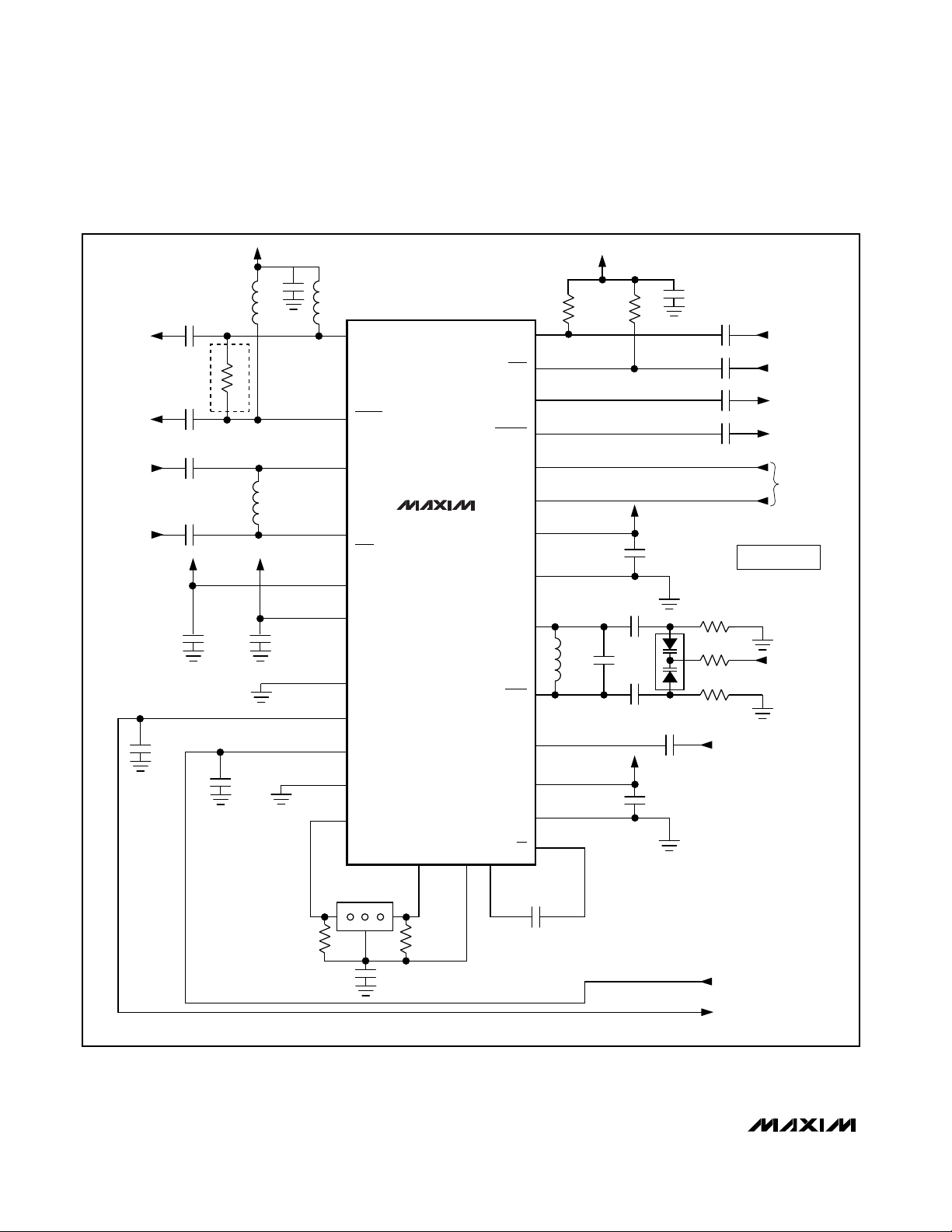
___________________________________________________Typical Operating Circuit
TXOUT TXIN
TXIN
LIMOUT
RXEN
TXEN
V
CC
GND
TANK
TANK
OSCOUT
V
CC
V
CC
V
CC
GND
VREFLIMIN CZ
CZ
LIMOUT
TXOUT
RXIN
RXIN
GND
RSSI
GC
GND
MIXOUT
24
13
14
18
17
7
6
9
8
V
CC
L
CHOKE
L
CHOKE
C
BLOCK
C
BLOCK
C
MATCH
C
MATCH
V
CC
V
CC
L
MATCH
Tx
OUTPUT
V
CC
Rx
INPUT
R*
D1
10kΩ
10kΩ
10kΩ
23
25
22
20
21
20
4
5
26
27
47nF47nF
0.01µF*
100pF
MAX2511
8.2nH 12pF
6.8 pF
6.8pF
16
15
47nF
1k1k
V
CC
INPUT
10.7MHz Tx
IF OUTPUT
CONTROL
LOGIC
VCO ADJUST
FROM PLL
47nF
10.7MHz Rx
0.1µF
0.1µF
0.1µF
0.1µF
12
TO PRESCALER
GAIN CONTROL VOLTAGE
RSSI OUTPUT
470pF
10
3
2281
0.1µF
330Ω
*
OPTIONAL
330Ω
11
V
CC
47nF
0.01µF
10.7MHz
BPF, Z0 = 330Ω
F
OSC
= 435.7MHz
D1 = ALPHA SMV1204-199
47nF
 Loading...