

Page 1
________________General Description
The MAX2510 is a highly integrated IF transceiver for
digital wireless applications. It operates from a +2.7V to
+5.5V supply voltage and features four operating
modes for advanced system power management.
Supply current is reduced to 0.2µA in shutdown mode.
In a typical application, the receiver downconverts a
high IF/RF (up to 600MHz) to a low IF (up to 30MHz)
using a double-balanced mixer. Additional functions
included in the receiver section are an IF buffer that
can drive an off-chip filter, an on-chip limiting amplifier
offering 90dB of received-signal-strength indication
(RSSI), and a robust differential limiter output driver
designed to directly drive a CMOS input. The transmitter section upconverts I and Q baseband signals to an
IF in the 100MHz to 600MHz range using a quadrature
modulator. The transmit output is easily matched to
drive a SAW filter with an adjustable output from 0dBm
to -40dBm and excellent linearity.
The MAX2511 has features similar to the MAX2510, but
upconverts a low IF with an image-reject mixer. The
MAX2511 downconverter also offers image rejection
with a limiter/RSSI stage similar to that of the MAX2510.
________________________Applications
PWT1900, Wireless Handsets, and Base Stations
PACS, PHS, DECT, and Other PCS Wireless
Handsets and Base Stations
400MHz ISM Transceivers
IF Transceivers
Wireless Data Links
____________________________Features
♦ +2.7V to +5.5V Single-Supply Operation
♦ Complete Receive Path: 600MHz (max) 1st IF to
30MHz (max) 2nd IF
♦ Unique, Wide-Dynamic-Range Downconverter
Mixer Offers -8dBm IIP3, 11dB NF
♦ 90dB Dynamic-Range Limiter with High-Accuracy
RSSI Function
♦ Differential Limiter Output Directly Drives
CMOS Input
♦ 100MHz to 600MHz Transmit Quadrature
Modulator with 41dB Sideband Suppression
♦ 40dB Transmit Gain-Control Range; Up to +1dBm
Output Power
♦ Advanced Power Management (four modes)
♦ 0.2µA Shutdown Supply Current
MAX2510
Low-Voltage IF Transceiver with
Limiter/RSSI and Quadrature Modulator
________________________________________________________________ Maxim Integrated Products 1
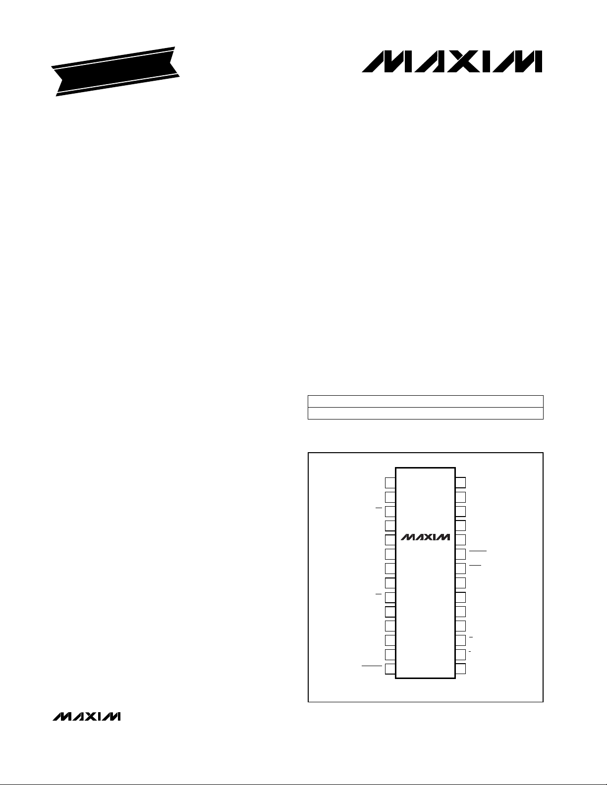
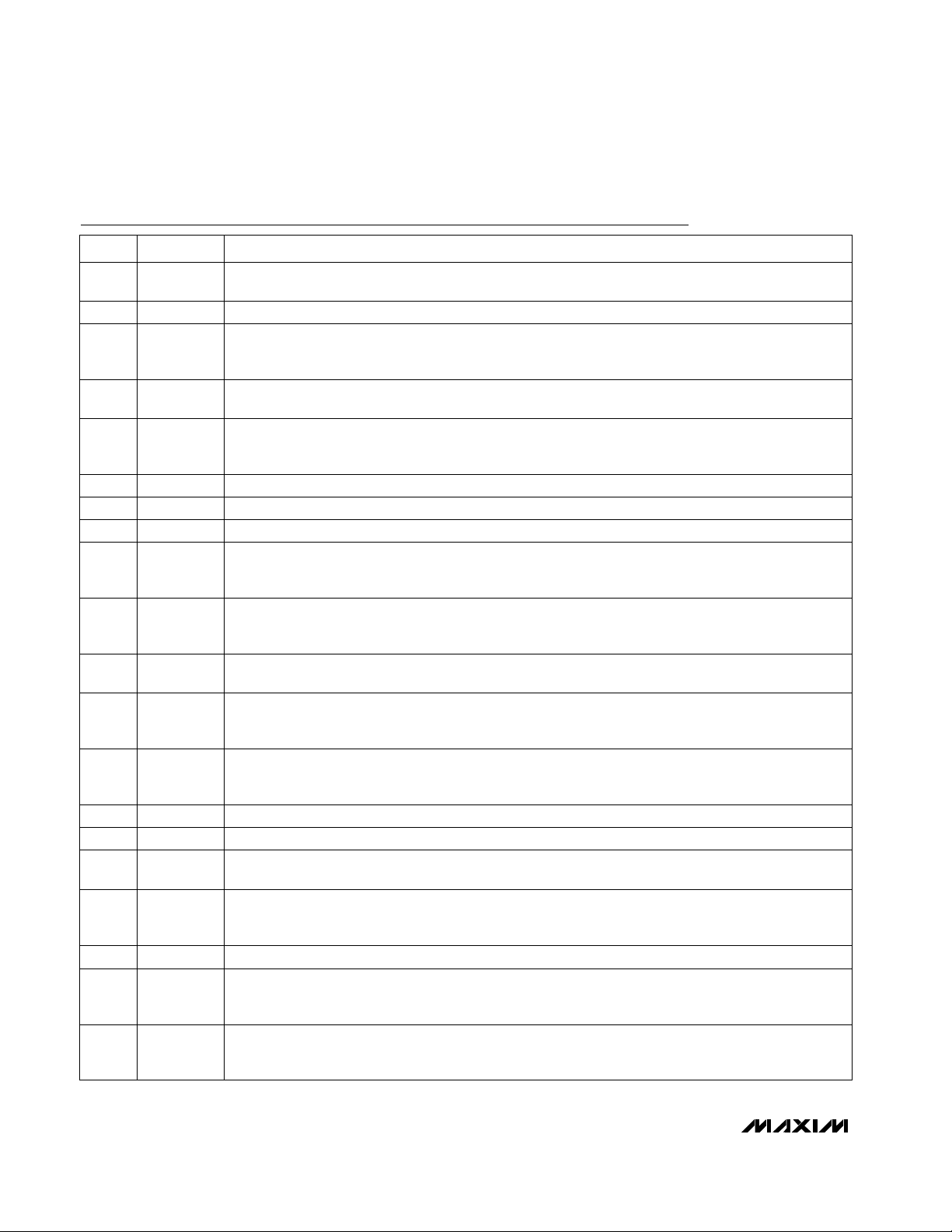
___________________Pin Configuration
19-1296; Rev 2; 1/01
PART
MAX2510EEI -40°C to +85°C
TEMP. RANGE PIN-PACKAGE
28 QSOP
EVALUATION KIT MANUAL
FOLLOWS DATA SHEET
_______________Ordering Information
Typical Operating Circuit appears on last page.
For price, delivery, and to place orders, please contact Maxim Distribution at 1-888-629-4642,
or visit Maxim’s website at www.maxim-ic.com.
TOP VIEW
LIMIN
RSSI
GND
V
GND
TXEN
RXEN
LIMOUT
LIMOUT
1
2
CZ
3
CZ
4
5
GC
LO
CC
LO
MAX2510
6
7
8
9
10
11
12
13
14
QSOP
28
27
26
25
24
23
22
21
20
19
18
17
16
15
VREF
MIXOUT
GND
RXIN
TXOUT
TXOUT
RXIN
V
CC
GND
V
CC
Q
Q
I
I
Page 2
MAX2510
Low-Voltage IF Transceiver with
Limiter/RSSI and Quadrature Modulator
2 _______________________________________________________________________________________
ABSOLUTE MAXIMUM RATINGS
DC ELECTRICAL CHARACTERISTICS
(VCC= +2.7V to +5.5V; 0.01µF across CZ and CZ; LO, LO open; MIXOUT tied to VREF through a 165Ω resistor; GC = 0.5V; RXIN,
RXIN open; LIMIN tied through 50Ω to VREF; LIMOUT, LIMOUT = open; RXEN, TXEN = high; bias voltage at I, I, Q, Q = 1.4V;
T
A
= -40°C to +85°C; unless otherwise noted. Typical values are at TA= +25°C.)
AC ELECTRICAL CHARACTERISTICS
(MAX2510 test fixture; VCC= +3.0V; RXEN = TXEN = low; 0.01µF across CZ and CZ; MIXOUT tied to VREF through 165Ω resistor;
TXOUT and TXOUT loaded with 100Ω differential; LO terminated with 50Ω, LO AC grounded; GC open; LIMOUT, LIMOUT are AC
coupled to 250Ω load; 330pF at RSSI pin; 0.1µF connected from VREF pin to GND; P
RXIN, RXIN
= -30dBm differentially driven (input
matched); f
RXIN, RXIN
= 240MHz; bias voltage at I, I, Q, Q = 1.4V; V
I,Q
= 500mVp-p; f
I,Q
= 200kHz; f
LO, LO
= 230MHz; P
LO
= -13dBm;
T
A
= +25°C; unless otherwise noted.)
Stresses beyond those listed under “Absolute Maximum Ratings” may cause permanent damage to the device. These are stress ratings only, and functional
operation of the device at these or any other conditions beyond those indicated in the operational sections of the specifications is not implied. Exposure to
absolute maximum rating conditions for extended periods may affect device reliability.
VCCto GND .............................................................-0.3V to 8.0V
V
CC
to Any Other VCC........................................................±0.3V
I, I, Q, Q to GND.........................................-0.3V to (V
CC
+ 0.3V)
I to I, Q to Q Differential Voltage............................................±2V
RXIN to RXIN Differential Voltage..........................................±2V
LOIN to LOIN Differential Voltage..........................................±2V
LIMIN Voltage .............................(VREF - 1.3V) to (VREF + 1.3V)
RXEN, TXEN, GC Voltage...........................-0.3V to (V
CC
+ 0.3V)
RXEN, TXEN, GC Input Current ............................................1mA
RSSI Voltage...............................................-0.3V to (V
CC
+ 0.3V)
Continuous Power Dissipation (T
A
= +70°C)
QSOP (derate 10mW/°C above +70°C)........................650mW
Operating Temperature Range ...........................-40°C to +85°C
Junction Temperature......................................................+150°C
Storage Temperature Range .............................-65°C to +165°C
Lead Temperature (soldering, 10sec) .............................+300°C
CONDITIONS
V2.7 3.0 5.5Operating Voltage Range
UNITSMIN TYP MAXPARAMETER
RXEN, TXEN V2.0Digital Input Voltage High
RXEN, TXEN = 2.0V µA
630
Digital Input Current High
RXEN, TXEN V0.4Digital Input Voltage Low
Receive mode, RXEN = high, TXEN = low
14 20
Standby mode, RXEN = high, TXEN = high
mA
0.5 1
RXEN, TXEN = 0.4V
Transmit mode, RXEN = low, TXEN = high
17 25
µA-5 0.1Digital Input Current Low
Shutdown mode, RXEN = low, TXEN = low µA
0.2 5
Supply Current
V
VCC/ 2 -
V
CC
/ 2
V
CC
/ 2 +
100mV 100mV
VREF Voltage
(Note 1) kΩ
50 85
GC Input Resistance
(Note 2) MHz100 600Input Frequency Range
Single sideband dB11Noise Figure
TA= +25°C
dB
20.5 22.5 25
Conversion Gain
CONDITIONS
(Note 4) dBm-18.5Input 1dB Compression Point
Two tones at 240MHz and 240.2MHz,
-30dBm per tone
dBm-8Input Third-Order Intercept
UNITSMIN TYP MAXPARAMETER
dBc49LO to RXIN Isolation
Standby to RX or TX (Note 5) µs5Power-Up Time
DOWNCONVERTER (RXEN = high)
19.9 25.5
TA= -40°C to +85°C (Note 3)
Page 3
MAX2510
Low-Voltage IF Transceiver with
Limiter/RSSI and Quadrature Modulator
_______________________________________________________________________________________ 3
AC ELECTRICAL CHARACTERISTICS (continued)
(MAX2510 test fixture; VCC= +3.0V; RXEN = TXEN = low; 0.01µF across CZ and CZ; MIXOUT tied to VREF through 165Ω resistor;
TXOUT and TXOUT loaded with 100Ω differential; LO terminated with 50Ω, LO AC grounded; GC open; LIMOUT, LIMOUT are AC
coupled to 250Ω load; 330pF at RSSI pin; 0.1µF connected from VREF pin to GND; P
RXIN, RXIN
= -30dBm differentially driven (input
matched); f
RXIN, RXIN
= 240MHz; bias voltage at I, I, Q, Q = 1.4V; V
I,Q
= 500mVp-p; f
I,Q
= 200kHz; f
LO, LO
= 230MHz; P
LO
= -13dBm;
T
A
= +25°C; unless otherwise noted.)
Note 1: This pin is internally terminated to approximately 1.35V through the specified resistance.
Note 2: Downconverter gain is typically greater than 20dB. Operation outside this frequency range is possible but has not been
characterized.
Note 3: Guaranteed by design and characterization.
LIMOUT, LIMOUT
mV±270 ±300 ±350
-85dBm to 5dBm
Limiter Output Voltage Swing
-75dBm to 5dBm degrees±4.5
dB
Phase Variation
90Minimum Monotonic RSSI Range
-75dBm to 5dBm from 50Ω mV/dB20RSSI Slope
CONDITIONS
-75dBm to 5dBm dB80Minimum Linear RSSI Range
UNITSMIN TYP MAXPARAMETER
(Note 6) dBm-86
At LIMIN input of +5dBm
RSSI Maximum Zero-Scale Intercept
TA= +25°C
dB
±0.5 ±2.0
V
RSSI Relative Error (Notes 6, 7)
1.8Maximum-Scale RSSI Voltage
At LIMIN input of -75dBm V0.25Minimum-Scale RSSI Voltage
I, I, Q, Q inputs are 250mVp-p centered around
this voltage, GC = 2.0V (Note 9)
(Note 8) MHz100 600Frequency Range
1.3
V
CC
-
1.2
I, I, Q, Q Allowable Common-Mode
Voltage Range
GC = 0.5V -41
GC = 2.0V (Note 9)
GC = open -16
-3
90° phase difference between I and Q inputs;
GC = 2V
dBc30 40Unwanted Sideband Suppression
dBm
-2.5 1
Output Power
GC = 2V (Note 11) -33
Output IM3 Level
GC = 2V (Note 11) dBc-51Output IM5 Level
GC = 0.5V (Note 11)
dBc
-49
I, Q are 500mVp-p while I, Q are held at this DC
voltage (Note 9)
1.4
V
CC
-
1.3
90° phase difference between I and Q inputs;
measured to fundamental tone; GC = 2V
dBc30 44LO Rejection
V
TA= -40°C to +85°C (Note 3) ±3.0
TA= +25°C
(Note 3) MHz70 80
I, I, Q, Q 1dB Bandwidth
LIMITING AMPLIFIER AND RSSI (RXEN = high, f
LIMIN
= 10MHz, P
LIMIN
= -30dBm from 50Ω source, unless otherwise noted)
TRANSMITTER (TXEN = high)
TA= -40°C to +85°C
Page 4
MAX2510
Low-Voltage IF Transceiver with
Limiter/RSSI and Quadrature Modulator
4 _______________________________________________________________________________________
__________________________________________Typical Operating Characteristics
(MAX2510 EV kit; VCC= +3.0V; 0.01µF across CZ and CZ; MIXOUT tied to VREF through 165Ω resistor; TXOUT and TXOUT loaded
with 100Ω differential; LO terminated with 50Ω; LO AC grounded; GC open; LIMOUT, LIMOUT open; 330pF at RSSI pin; 0.1µF connected from VREF pin to GND; P
RXIN, RXIN
= -30dBm differentially driven (input matched); f
RXIN, RXIN
= 240MHz; bias voltage at I, I,
Q, Q = 1.4V; V
I,Q
= 500mVp-p; f
I, Q
= 200kHz; f
LO, LO
= 230MHz; PLO= -13dBm; TA= +25°C; unless otherwise noted.)
0
5
15
10
20
Rx
Tx
25
-40 0-20 20406080100
SUPPLY CURRENT
vs. TEMPERATURE
MAX2510toc01
TEMPERATURE (°C)
SUPPLY CURRENT (mA)
STANDBY
0
6
4
2
8
10
12
14
16
18
20
2.5 3.53.0 4.0 4.5 5.0 5.5
SUPPLY CURRENT
vs. SUPPLY VOLTAGE
MAX2510toc02
SUPPLY VOLTAGE (V)
SUPPLY CURRENT (mA)
Rx
STANDBY
Tx
10
5
0
15
25
20
30
35
00.40.2 0.6 1.21.00.8 1.4 1.6 1.8 2.0
TRANSMITTER SUPPLY CURRENT
vs. GC VOLTAGE
MAX2510toc03
GC VOLTAGE (V)
SUPPLY CURRENT (mA)
Note 4: Driving RXIN or RXIN with a power level greater than the 1dB compression level forces the input stage out of its linear
range, causing harmonic and intermodulation distortion. The RSSI output increases monotonically with increasing input
levels beyond the mixer’s 1dB compression level. Input 1dB compression point is limited by MIXOUT voltage swing, which
is approximately 2Vp-p into a 165Ω load.
Note 5: Assuming the supply voltage has been applied, this includes limiter offset-correction settling and Rx or Tx bias stabilization
time. Guaranteed by design and characterization.
Note 6: The RSSI maximum zero-scale intercept is the maximum (over a statistical sample of parts) input power at which the RSSI
output would be 0V. This point is extrapolated from the linear portion of the RSSI Output Voltage vs. Limiter Input Power
graph in the Typical Operating Characteristics. This specification and the RSSI slope define the RSSI function’s ideal
behavior (the slope and intercept of a straight line), while the RSSI relative error specification defines the deviations from
this line. See the Typical Operating Characteristics for the RSSI Output Voltage vs. Limiter Input Power graph.
Note 7: The RSSI relative error is the deviation from the best-fitting straight line of the RSSI output voltage versus the limiter input
power. This number represents the worst-case deviation at any point along this line. A 0dB relative error is exactly on the
ideal RSSI transfer function. The limiter input power range for this test is -75dBm to 5dBm from 50Ω. See the Typical
Operating Characteristics for the RSSI Relative Error graph.
Note 8: Transmit sideband suppression is typically better than 35dB. Operation outside this frequency range is possible but has
not been characterized.
Note 9: Output IM3 level is typically better than -29dBc.
Note 10: The output power can be increased by raising GC above 2V. Refer to the Transmitter Output Power vs. GC Voltage and
Frequency graph in the Typical Operating Characteristics.
Note 11: Using two tones at 400kHz and 500kHz, 250mVp-p differential per tone at I, I, Q, Q.
Page 5

MAX2510
Low-Voltage IF Transceiver with
Limiter/RSSI and Quadrature Modulator
_______________________________________________________________________________________ 5
____________________________ Typical Operating Characteristics (continued)
(MAX2510 EV kit; VCC= +3.0V; 0.01µF across CZ and CZ; MIXOUT tied to VREF through 165Ω resistor; TXOUT and TXOUT loaded
with 100Ω differential; LO terminated with 50Ω; LO AC grounded; GC open; LIMOUT, LIMOUT open; 330pF at RSSI pin; 0.1µF connected from VREF pin to GND; P
RXIN, RXIN
= -30dBm differentially driven (input matched); f
RXIN, RXIN
= 240MHz; bias voltage at I, I,
Q, Q = 1.4V; V
I,Q
= 500mVp-p; f
I, Q
= 200kHz; f
LO, LO
= 230MHz; PLO= -13dBm; TA= +25°C; unless otherwise noted.)
SHUTDOWN SUPPLY CURRENT
vs. SUPPLY VOLTAGE
1.2
1.0
0.8
0.6
0.4
SHUTDOWN SUPPLY CURRENT (µA)
0.2
0
TA = +85°C
TA = -40°C
TA = +25°C
2.5 3.5 4.03.0 4.5 5.0 5.5
SUPPLY VOLTAGE (V)
DOWNCONVERTER MIXER CONVERSION
GAIN vs. SUPPLY VOLTAGE
AND TEMPERATURE
25
TA = -40°C
MAX2510toc04
24
23
22
GAIN (dB)
21
20
19
18
2.5 3.5 4.03.0 4.5 5.0 5.5
T
= +25°C
A
VOLTAGE (V)
TA = +85°C
MAX2510toc05
DOWNCONVERTER MIXER CONVERSION
GAIN vs. RXIN FREQUENCY
25
20
15
GAIN (dB)
10
5
0
0 400 500200 300100 600 700 800 900 1000
RF FREQUENCY (MHz)
MISMATCH LOSS
COMPENSATED
MAX2510toc06
RECEIVE MIXER INPUT 1dB
COMPRESSION POINT vs. SUPPLY VOLTAGE
-12
-13
-14
-15
-16
-17
-18
-19
INPUT 1dB COMPRESSION (dBm)
-20
-21
-22
2.5 3.53.0 4.0 4.5 5.0 5.5
SUPPLY VOLTAGE (V)
TA = +85°C
TA = +25°C
TA = -40°C
MAX2510toc07
RXIN INPUT IMPEDANCE
500
450
400
)
350
Ω
300
250
200
REAL IMPEDANCE (
150
100
50
0
30 150 21090 270 330 390 450 510
vs. FREQUENCY
SINGLE-ENDED
IMAGINARY
REAL
FREQENCY (MHz)
MAX2510toc08
Page 6

MAX2510
Low-Voltage IF Transceiver with
Limiter/RSSI and Quadrature Modulator
6 _______________________________________________________________________________________
____________________________ Typical Operating Characteristics (continued)
(MAX2510 EV kit; VCC= +3.0V; 0.01µF across CZ and CZ; MIXOUT tied to VREF through 165Ω resistor; TXOUT and TXOUT loaded
with 100Ω differential; LO terminated with 50Ω; LO AC grounded; GC open; LIMOUT, LIMOUT open; 330pF at RSSI pin; 0.1µF connected from VREF pin to GND; P
RXIN, RXIN
= -30dBm differentially driven (input matched); f
RXIN, RXIN
= 240MHz; bias voltage at I, I,
Q, Q = 1.4V; V
I,Q
= 500mVp-p; f
I, Q
= 200kHz; f
LO, LO
= 230MHz; PLO= -13dBm; TA= +25°C; unless otherwise noted.)
RSSI OUTPUT VOLTAGE vs. LIMIN INPUT
2.0
1.8
1.6
1.4
1.2
1.0
0.8
RSSI VOLTAGE (V)
0.6
0.4
0.2
0
-120 -100 -80 -60 -40 -20 0 20
POWER AND TEMPERATURE
V
= +85°C
OUT
V
= -40°C
OUT
LIMITER INPUT POWER (dBm, 50Ω)
10
0
-10
-20
-30
OUTPUT POWER (dBm)
-40
-50
-60
0.5 0.9 1.10.7 1.3 1.5 1.7 1.9
-30
V
= +25°C
OUT
TRANSMITTER OUTPUT POWER
vs. GC VOLTAGE AND FREQUENCY
230MHz
200MHz
GC VOLTAGE (V)
TRANSMITTER IM3 LEVELS
vs. GC VOLTAGE
RSSI RELATIVE ERROR vs. LIMIN INPUT
POWER AND TEMPERATURE
5
4
MAX2510toc10a
RSSI ERROR (dB)
500MHz
3
2
1
0
-1
-2
-3
-4
-5
-95 -75 -55 -35 -15 5
TA = -40°C
T
A
TA = +25°C
TA = +85°C
LIMITER INPUT POWER (dBm, 50Ω)
MAX2510toc12
= +25°C
MAX2510toc10
5
0
-5
-10
-15
OUTPUT POWER (dBm)
-20
-25
0400200 600 800 1000
TRANSMITTER OUTPUT 1dB COMPRESSION
10
RSSI OUTPUT VOLTAGE
2.0
1.8
1.6
1.4
1.2
1.0
0.8
RSSI VOLTAGE (V)
0.6
0.4
0.2
0
vs. RXIN INPUT POWER
-80 -60 -50 -40-70 -30 -20 -10 0
RXIN INPUT POWER (dBm)
TRANSMITTER OUTPUT POWER
vs. FREQUENCY
GC = 2.0V
FREQUENCY (MHz)
POINT vs. GC VOLTAGE
MAX2510toc12a
MAX2510toc11
-35
-40
-45
IM3 LEVELS (dBc)
-50
-55
0 0.8 1.00.4 0.60.2 1.2 1.4 1.6 1.8 2.0
GC VOLTAGE (V)
MAX2510toc13
0
-10
-20
-30
-40
OUTPUT 1dB COMPRESSION (dBm)
-50
-60
TA = +85°C
TA = -40°C
TA = +25°C
0 0.40.2 0.6 1.21.00.8 1.4 1.6 1.8 2.0
GC VOLTAGE (V)
MAX2510toc15
Page 7

MAX2510
Low-Voltage IF Transceiver with
Limiter/RSSI and Quadrature Modulator
_______________________________________________________________________________________ 7
____________________________ Typical Operating Characteristics (continued)
(MAX2510 EV kit; VCC= +3.0V; 0.01µF across CZ and CZ; MIXOUT tied to VREF through 165Ω resistor; TXOUT and TXOUT loaded
with 100Ω differential; LO terminated with 50Ω; LO AC grounded; GC open; LIMOUT, LIMOUT open; 330pF at RSSI pin; 0.1µF connected from VREF pin to GND; P
RXIN, RXIN
= -30dBm differentially driven (input matched); f
RXIN, RXIN
= 240MHz; bias voltage at I, I,
Q, Q = 1.4V; V
I,Q
= 500mVp-p; f
I, Q
= 200kHz; f
LO, LO
= 230MHz; PLO= -13dBm; TA= +25°C; unless otherwise noted.)
TRANSMITTER OUTPUT POWER
1.0
0.8
0.6
0.4
OUTPUT POWER (dBm)
0.2
0
2.5 3.53.0 4.0 4.5 5.0 5.5
vs. SUPPLY VOLTAGE
SUPPLY VOLTAGE (V)
TRANSMITTER DIFFERENTIAL
OUTPUT IMPEDANCE vs. FREQUENCY
100
Tx MODE REAL
0
-100
-200
-300
-400
Tx OFF
-500
IMAGINARY
-600
-700
-800
REAL AND IMAGINARY IMPEDANCE (Ω)
-900
-1000
200 400300 500
Tx OFF REAL
Tx MODE
IMAGINARY
FREQUENCY (MHz)
TA = +25°C
TA = +85°C
TA = -40°C
vs. BASEBAND INPUT VOLTAGE
-10
GC = OPEN
-12
MAX2510toc15
-14
-16
-18
-20
-22
OUTPUT POWER (dBm)
-24
-26
-28
-30
50 100 150 200 250 300 350 400
-134
Af = 200kHz
-136
MAX2510toc18
-138
-140
-142
-144
-146
-148
OUTPUT NOISE POWER (dBm/Hz)
-150
-152
-154
0 0.4 0.6 0.80.2 1.0 1.2 1.4 1.81.6 2.0
OUTPUT POWER
BASEBAND INPUT VOLTAGE (mVp)
TRANSMIT NOISE POWER
vs. GC VOLTAGE
GC VOLTAGE (V)
TRANSMITTER SIDEBAND SUPPRESSION
50
MAX2510toc16
40
30
20
SIDEBAND SUPPRESSION (dB)
10
0
0 400200 600 800 1000
-13.0
-13.5
MAX2510toc19
-14.0
-14.5
-15.0
-15.5
-16.0
OUTPUT POWER (dBm)
-16.5
-17.0
-17.5
-18.0
-20 -16 -14 -12-18 -10 -8 -6 -2-4 0
vs. RF FREQUENCY
MAX2510toc17
RF FREQUENCY (MHz)
TRANSMITTER OUTPUT POWER
vs. LO POWER
MAX2510toc20
LO POWER (dBm)
Page 8
MAX2510
Low-Voltage IF Transceiver with
Limiter/RSSI and Quadrature Modulator
8 _______________________________________________________________________________________
Pin Description
PIN
Offset-Correction Capacitor Pins. Connect a 0.01µF capacitor between CZ and CZ.CZ, CZ
2, 3
Limiter Input. Connect a 330Ω (typical) resistor to VREF for DC bias, as shown in the Typical Operating
Circuit.
LIMIN1
FUNCTIONNAME
Gain-Control Pin. Applying a DC voltage to GC between 0V and 2.0V adjusts the transmitter gain by
more than 40dB. GC is internally terminated to 1.35V via an 85kΩ resistor.
GC5
Received Signal-Strength Indicator Output. The voltage on RSSI is proportional to the signal power at
LIMIN. The RSSI output sources current pulses into a 330pF (typical) external capacitor. This output is
internally terminated with 11kΩ, and this RC time constant sets the decay time.
RSSI4
Local-Oscillator Input Ground. Connect to PC board ground plane with minimal inductance.GND7
Differential LO Inputs. In a typical application, externally terminate LO with 50Ω to ground, then AC couple into LO. AC terminate LO directly to ground for single-ended operation, as shown in the Typical
Operating Circuit.
LO, LO
6, 9
Baseband In-Phase Inputs. The differential voltage across these inputs forms the quadrature modulator’s
I-channel input. The signal input level is typically up to 500mVp-p centered around a 1.4V (typical) DC
bias level on I.
I, I
15, 16
Differential Outputs of the Limiting Amplifier. These outputs are complementary emitter followers capable
of driving 250Ω single-ended loads to ±300mV.
LIMOUT,
LIMOUT
13, 14
Baseband Quadrature-Phase Inputs. The differential voltage across these inputs forms the quadrature
modulator’s Q-channel input. The signal input level is typically up to 500mVp-p, centered around a 1.4V
(typical) DC bias level on Q.
Q, Q
17, 18
Receiver Enable Pin. When high, RXEN enables the receiver if TXEN is low. If both RXEN and TXEN are
high, the part is in standby mode; if both are low, the part is in shutdown. See the Power Management
section for details.
RXEN12
Transmitter-Enable Pin. When high, TXEN enables the transmitter if RXEN is low. If both TXEN and
RXEN are high, the part is in standby mode; if both are low, the part is in shutdown. See the Power
Management section for details.
TXEN11
Differential Outputs of the Upconverter. In a typical application, these open-collector outputs are pulled
up to V
CC
with two external inductors and AC coupled to the load. See the Applications Information sec-
tion for more details, including information on impedance matching these outputs to a load.
TXOUT,
TXOUT
23, 24
Differential Inputs of the Downconverter Mixer. An impedance-matching network may be required in
some applications. See the Applications Information section for details.
RXIN,
RXIN
22, 25
Reference Voltage Pin. VREF provides an external bias voltage for the MIXOUT and LIMIN pins. Bypass
this pin with a 0.1µF capacitor to ground. The VREF voltage is equal to V
CC
/ 2. See the Typical
Operating Circuit for more information.
VREF28
Receiver Mixer Ground. Connect to PC board ground plane with minimal inductance.GND26
General-Purpose VCCPins. Bypass with a 0.047µF low-inductance capacitor to GND.V
CC
19, 21
Local-Oscillator Input VCCPin. Bypass directly to local-oscillator input ground (pin 8).V
CC
8
Limiter Ground. Connect to PC board ground plane with minimal inductance.GND10
Receiver/Transmitter Ground. Connect to PC board ground plane with minimal inductance.GND20
Single-Ended Output of the Downconverter Mixer. This pin is high-impedance and must be biased to the
VREF pin through an external terminating resistor whose value depends on the interstage filter characteristics. See the Applications Information section for details.
MIXOUT27
Page 9

_______________Detailed Description
The following sections describe each of the blocks
shown in Figure 1.
Receiver
The receiver consists of two basic blocks: the downconverter mixer and the limiter/received-signal-strength
indicator (RSSI) section.
The receiver inputs are the RXIN and RXIN pins, which
should be AC coupled and may require a matching
network as shown in the Typical Operating Circuit. To
design a matching network for a particular application,
consult the RXIN Input Impedance plots in the Typical
Operating Characteristics, as well as the Applications
Information sections.
Downconverter Mixer
The downconverter consists of an a double-balanced
mixer and an output buffer. The MIXOUT output, a singleended current source, can drive a shunt-terminated
330Ω filter (165Ω load) to more than 2Vp-p over the
entire supply range, providing excellent dynamic
range. The local oscillator (LO) input is buffered and
drives the mixer.
Limiter
The signal passes through an external IF bandpass filter into the limiter input (LIMIN). LIMIN is a singleended input that is biased at the VREF pin voltage. The
open-circuit input impedance is typically greater than
10kΩ to VREF. For proper operation, LIMIN must be
tied to VREF through the filter-terminating impedance
(which should be less than 1kΩ). The limiter provides a
constant output level, which is largely independent of
the limiter input signal level over a 90dB input range.
The low-impedance limiter outputs provide 600mVp-p
single-ended swing (1.2Vp-p differential swing) and
can drive CMOS inputs directly.
MAX2510
Low-Voltage IF Transceiver with
Limiter/RSSI and Quadrature Modulator
_______________________________________________________________________________________ 9
Figure 1. Functional Diagram
RXIN
RXIN
LO
LO
RXEN
TXEN
GC
TXOUT
TXOUT
POWER
MANAGEMENT
PA
TRANSMIT VGA/PA
MIXOUT
g
m
VGA
IF BPF
LIMIN
VREF
VREF = V
Σ
/ 2
CC
0°
LO PHASE
90°
SHIFTER
CZ CZ
OFFSET
CORRECTION
LIMITER
RSSI
MAX2510
LIMOUT
LIMOUT
RSSI
I
I
Q
Q
Page 10
MAX2510
Received Signal-Strength Indicator
The RSSI output provides a linear indication of the
received power level on the LIMIN input. The RSSI
monotonic dynamic range exceeds 90dB while providing better than 80dB linear range. The RSSI output
pulses current into a 330pF (typical) external filter
capacitor. The output is internally terminated to ground
with 11kΩ, and this R-C time constant sets the decay
time. The rise time is limited by the RSSI pin’s output
drive current. The rise time is typically less than 100ns
with no capacitor connected. Larger capacitor values
slow the rise time.
Transmitter
The I, I and Q, Q baseband signals are input to a pair
of double-balanced mixers, which are driven from a
quadrature LO source. The quadrature LO is generated
on-chip from the oscillator input present at the LO and
LO pins. The two mixers’ outputs are summed. With
quadrature baseband inputs at the I, I and Q, Q pins,
the unwanted sideband is largely canceled. The resulting signal from the mixers is fed through a variable-gain
amplifier (VGA) with more than 40dB of gain-adjust
range.
The VGA output is connected to a driver amplifier with
an output 1dB compression point of +2dBm. The output power can be adjusted from approximately +2dBm
to -40dBm by controlling the GC pin. The resulting signal appears as a differential output on the TXOUT and
TXOUT pins.
TXOUT and TXOUT are open-collector outputs and
need external pull-up inductors to VCCfor proper operation, as well as a DC block so the load does not affect
DC biasing. A shunt resistor across TXOUT and TXOUT
(100Ω typical) can be used to back terminate an external filter, as shown in the Typical Operating Circuit.
Alternatively, a single-ended load can be connected to
TXOUT, as long as TXOUT is tied directly to VCC. Refer
to the Applications Information section for details.
Local-Oscillator Inputs
The MAX2510 requires an external LO source for the
mixers. LO and LO are high-impedance inputs (>1kΩ).
The external LO signal is buffered internally and fed to
both the receive mixer and the LO phase shifter used
for the transmit mixers.
In a typical application, externally terminate the LO
source with a 50Ω resistor and then AC couple into LO.
Typically, the LO power range should be -13dBm to
0dBm (into 50Ω). Connect a bypass capacitor from LO
to ground. Alternatively, a differential LO source (externally terminated) can drive LO and LO through series
coupling capacitors.
Power Management
To provide advanced system power management, the
MAX2510 features four operating modes that are
selected via the RXEN and TXEN pins, according to
Table 1 (supply currents assume GC = 0.5V).
In shutdown mode, all part functions are off. Standby
mode allows fastest enabling of either transmit or receive
mode by keeping the VREF generator active. This avoids
delays in stabilizing the limiter input circuitry and the offset correction loop. Transmit mode enables the LO
buffer, LO phase shifter, upconverter mixer, transmit
VGA, and transmit output driver amplifier. Receive mode
enables the LO buffer, downconverter mixer, limiting
amplifier, and RSSI functions.
__________Applications Information
RX Input Matching
The RXIN, RXIN port typically needs an impedance
matching network for proper connection to external circuitry, such as a filter. See the Typical Operating Circuit
for an example circuit topology. Note that the receiver
input can be driven either single-ended or differentially.
The component values used in the matching network
depend on the desired operating frequency as well as
on filter impedance. The following table indicates the
RXIN, RXIN single-ended input impedance (that is,
the impedance looking into either RXIN or RXIN). The
information in Table 2 is also plotted in the Typical
Operating Characteristics.
Low-Voltage IF Transceiver with
Limiter/RSSI and Quadrature Modulator
10 ______________________________________________________________________________________
High
Low
High
TXEN
STATE
Low
0.5m
14m
17m
TYPICAL
SUPPLY
CURRENT (A)
0.2µ
Standby
Receive
Transmit
MODE
Shutdown
High
High
Low
RXEN
STATE
Low
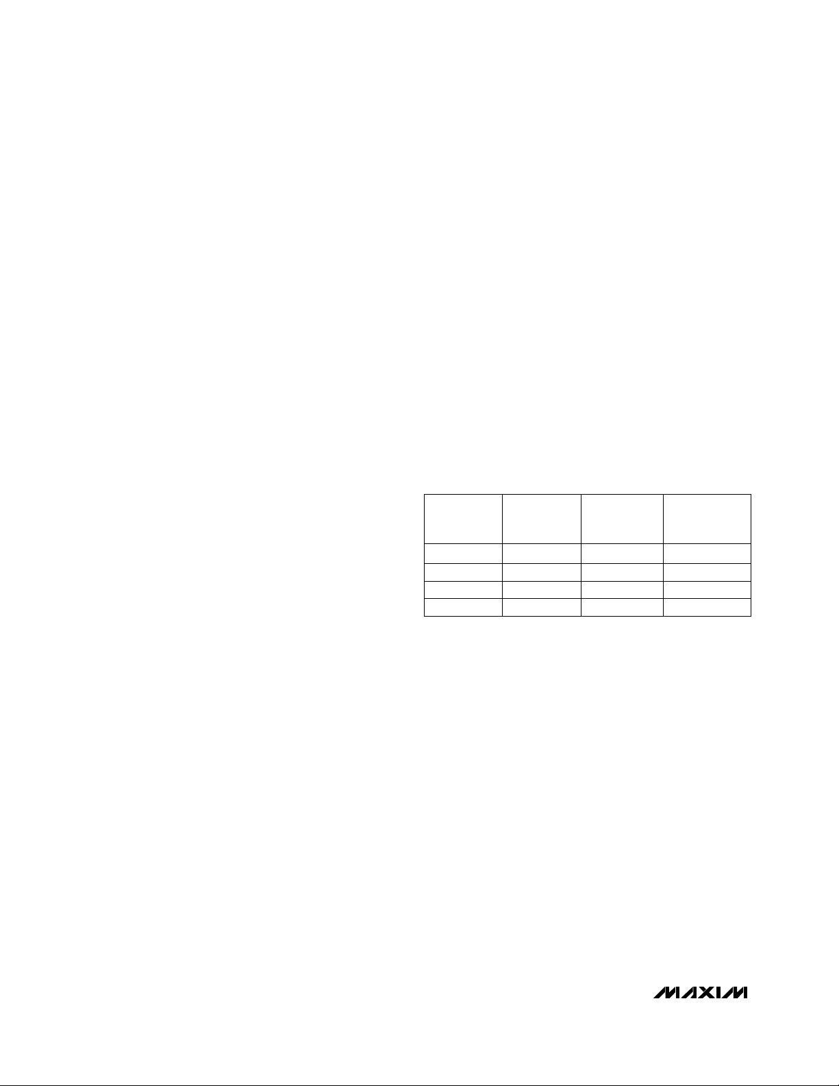
Table 1. Power-Supply Mode Selection
Page 11
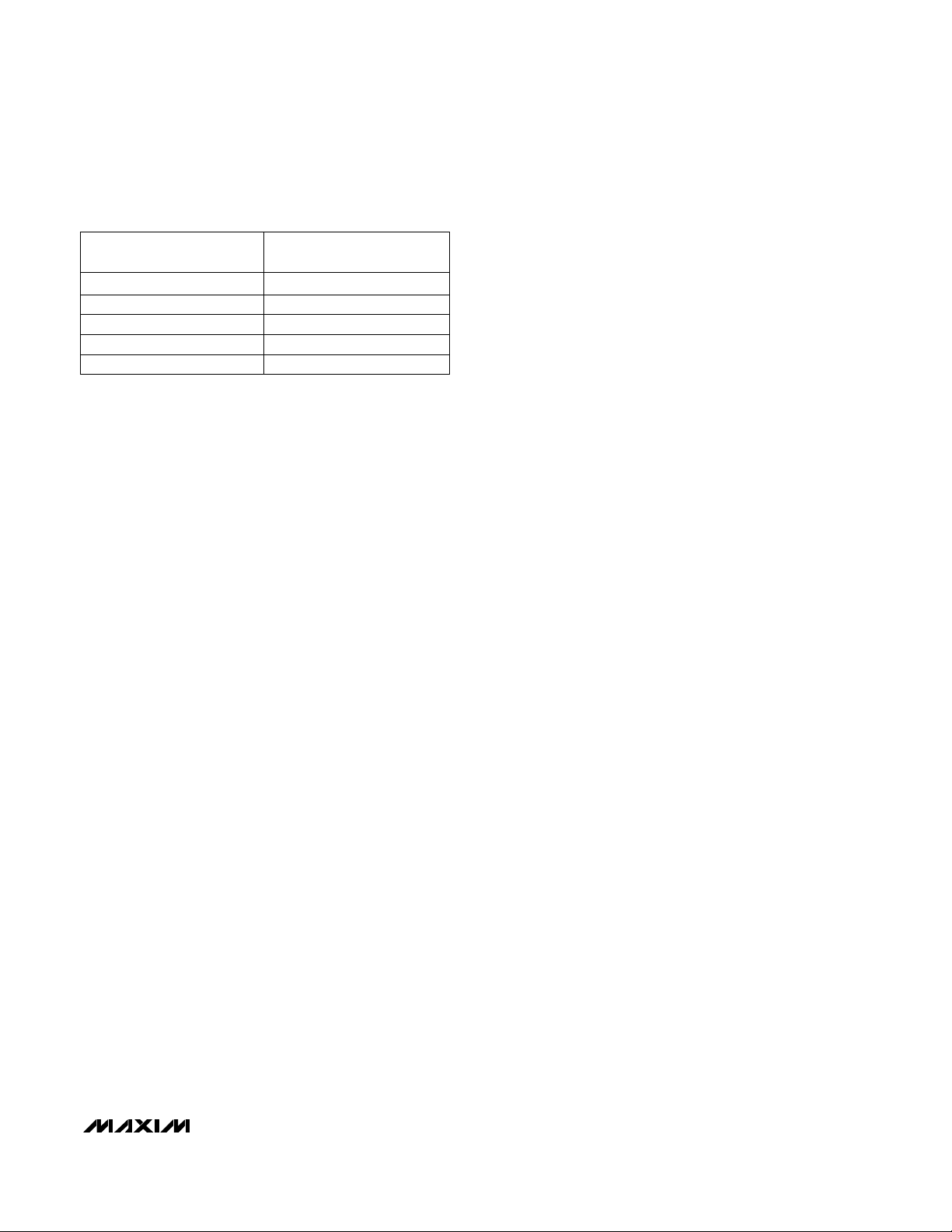
Table 2. RXIN or RXIN Input Impedance
Receive IF Filter
The interstage filter, located between the MIXOUT pin
and the LIMIN pin, is typically a three-terminal, 330Ω,
10.7MHz bandpass filter. This filter prevents the limiter
from acting on any undesired signals that are present
at the mixer’s output, such as LO feedthrough, out-ofband channel leakage, and spurious mixer products.
The filter connections are also set up to feed DC bias
from VREF into LIMIN and MIXOUT through two 330Ω
filter-termination resistors. (See the Typical Operating
Circuit for more information).
Transmit Output Matching
The transmit outputs, TXOUT and TXOUT, are opencollector outputs and therefore present a high
impedance.
For differential drive, TXOUT and TXOUT are connected
to V
CC
via chokes, and each side is AC coupled to the
load. A terminating resistor between TXOUT and
TXOUT sets the output impedance. This resistor provides a stable means of matching to the load.
TXOUT and TXOUT are voltage-swing limited, and
therefore cannot drive the specified maximum power
across more than 150Ω load impedance. This load
impedance typically consists of a shunt-terminating
resistor in parallel with a filter load impedance. To drive
higher output load impedances, the gain must be
reduced (via the GC pin) to avoid saturating the TX output stage.
For single-ended applications, connect the unused TX
output output pin directly to VCC.
400MHz ISM Applications
The MAX2510 can be used as a front-end IC in applications where the RF carrier frequency is in the
400MHz ISM band. In this case, Maxim recommends
preceding the MAX2510 receiver section with a low-
noise amplifier (LNA) that can operate over the same
supply voltage range. The MAX2630–MAX2633 family
of amplifiers meets this requirement. In many applications, the MAX2510’s transmit output power is sufficient
to eliminate the need for an external power amplifier.
______________________Layout Issues
A well-designed PC board is an essential part of an RF
circuit. Use the MAX2510 evaluation kit and the recommendations below as guides to generate your own
layout.
Power-Supply Layout
A star topology, which has a heavily decoupled central
VCCnode, is the ideal power-supply layout for minimizing coupling between different sections of the chip. The
VCCtraces branch out from this node, each going to
one VCCconnection in the MAX2510 typical operating
circuit. At the end of each of these traces is a bypass
capacitor that presents low impedance at the RF frequency of interest. This method provides local decoupling at each VCCpin. At high frequencies, any signal
leaking out of a supply pin sees a relatively high impedance (formed by the VCCtrace impedance) to the central VCCnode, and an even higher impedance to any
other supply pin, minimizing Vcc supply-pin coupling.
A single ground plane suffices. Where possible, multiple parallel vias aid in reducing inductance to the
ground plane.
Place the VREF decoupling capacitor (0.1µF typical) as
close to the MAX2510 as possible for best interstage filter performance. For best results, use a high-quality,
low-ESR capacitor.
Matching/biasing networks around the receive and
transmit pins should be symmetric and as close to the
chip as possible. A cutout in the ground plane under
the matching network components can be used to
reduce parasitic capacitance.
Decouple pins 19 and 21 (VCC) directly to pin 20 (Rx,
Tx ground), which should be directly connected the
ground plane. Similarly, decouple pin 8 directly to pin 7.
Refer to the Pin Description table for more information.
MAX2510
Low-Voltage IF Transceiver with
Limiter/RSSI and Quadrature Modulator
______________________________________________________________________________________ 11
64 - j109
94 - j143
149 - j184
SERIES IMPEDANCE
(Ω)
275 - j203
400
300
200
FREQUENCY
(MHz)
100
53 - j87500
Page 12

MAX2510
Low-Voltage IF Transceiver with
Limiter/RSSI and Quadrature Modulator
12 ______________________________________________________________________________________
Typical Operating Circuit
V
CC
FOR SINGLE-ENDED
TX OPERATION
100Ω
TX OUTPUT
(TO FILTER)
0.001µF
10pF
V
CC
0.001µF 0.001µF
220nH
MATCH
FOR SINGLE-ENDED
RX OPERATION
330pF
V
CC
100pF
V
CC
BpF, Z
23
24
25
22
26
21
19
20
27
10.7MHz
TXOUT
TXOUT
RXIN
RXIN
GND
V
CC
V
CC
GND
MIXOUT
= 330Ω
0
I
I
Q
MAX2510
LIMIN
128 2
VREF CZ
LIMOUT
LIMOUT
RXEN
TXEN
V
CC LO
GND
LOIN
LOIN
GND
RSSI
Q
LO
GC
CZ
15
16
18
17
13
14
12
11
8
7
6
9
10
5
4
3
0.01µF
47pF
V
CC
0.001µF
BASEBAND
I INPUT
BASEBAND
Q INPUT
RECEIVE IF
OUTPUT
CONTROL
LOGIC
47pF
330pF
5OΩ
0.001µF
FROM
LOCAL
OSCILLATOR
GAIN CONTROL
RSSI OUTPUT
IF
BYPASS
FILTER
330Ω
0.1µF
330Ω
 Loading...