

For free samples & the latest literature: http://www.maxim-ic.com, or phone 1-800-998-8800.
For small orders, phone 1-800-835-8769.
General Description
The MAX2472/MAX2473 are flexible, wideband, highreverse-isolation buffer amplifiers. The MAX2472 has dual
open-collector outputs capable of delivering -5dBm into
50Ω while maintaining harmonic suppression below
-25dBc. The MAX2473 has a single open-collector output
with a bias control pin to vary output power from -10dBm
to -2dBm while maintaining harmonic suppression below
-25dBc. The MAX2472/MAX2473’s combination of high
reverse isolation and low supply current makes them ideal
for applications requiring high performance with low
power. They feature high input impedance and open-collector outputs for maximum flexibility, enabling them to be
used with a variety of oscillator topologies.
Both the MAX2472 and MAX2473 operate from a single
+2.7V to +5.5V supply. With VCC= +3.0V and -25dBm
input power, the MAX2472 consumes 5.2mA, while the
MAX2473 consumes only 2.7mA. Both devices are available in a tiny 6-pin SOT23 package requiring minimal
board space.
Applications
Cellular and PCS Mobile Phones
Private Mobile Radios
ISM-Band Applications
IF/RF Oscillators
General-Purpose Buffers/Amplifiers
Typical Operating Circuits appear at end of data sheet.
Features
♦ +2.7V to +5.5V Supply Range
♦ 500MHz to 2500MHz Input Frequency Range
♦ High Reverse Isolation: 49dB at 900MHz
♦ Dual Open-Collector Outputs (MAX2472)
♦ Adjustable -10dBm to -2dBm Output Power
Control (MAX2473)
♦ High Input Impedance: >250Ω at 900MHz
♦ Ultra-Small SOT23-6 Package
MAX2472/MAX2473
500MHz to 2500MHz
VCO Buffer Amplifiers
________________________________________________________________
Maxim Integrated Products
1
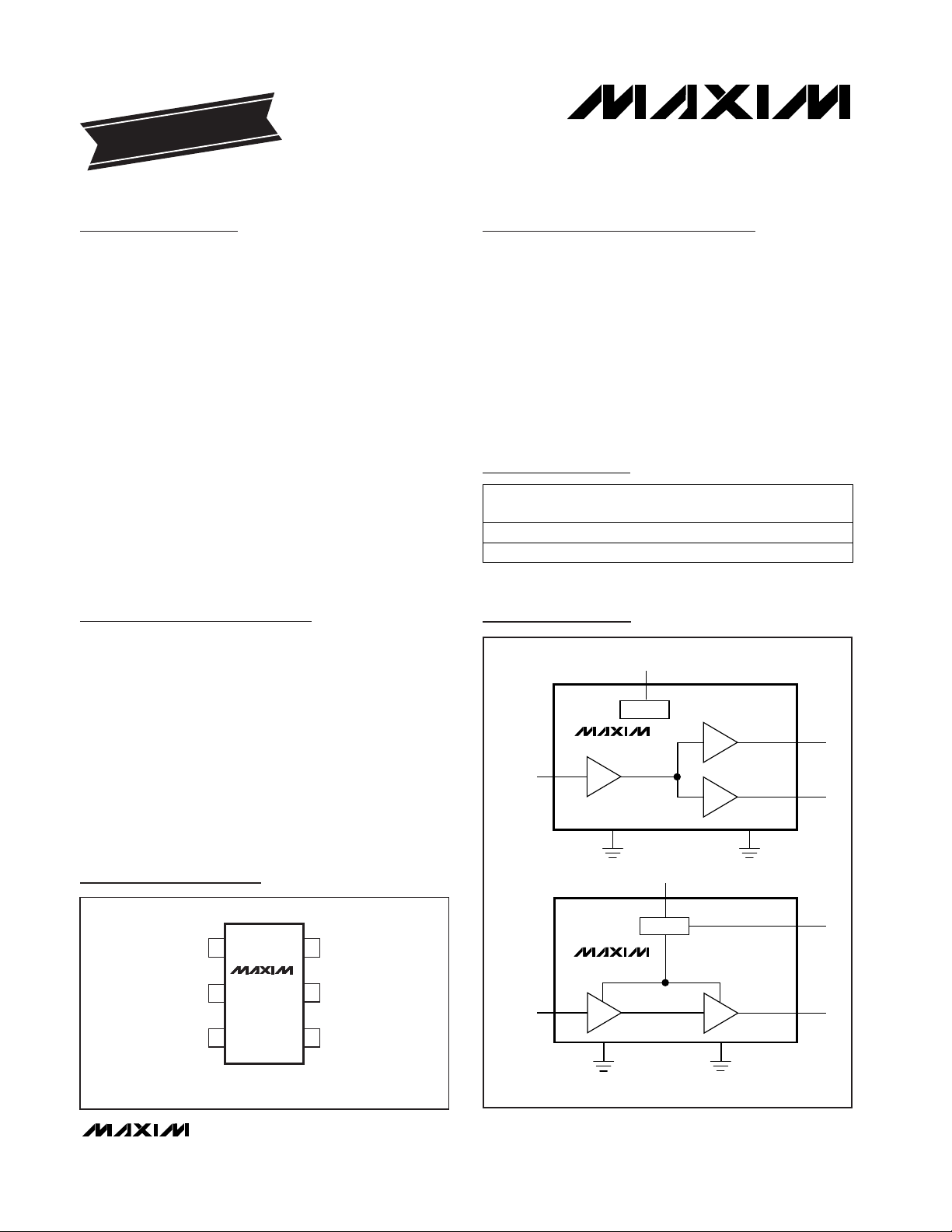
Functional Diagrams
19-1466; Rev 0; 6/99
PART
MAX2472EUT-T
MAX2473EUT-T
-40°C to +85°C
-40°C to +85°C
TEMP.
RANGE
PIN-
PACKAGE
6 SOT23-6
6 SOT23-6
EVALUATION KIT MANUAL
FOLLOWS DATA SHEET
Ordering Information
SOT
TOP MARK
AAAZ
AABA
GND
GND
OUT2
OUT1
IN
V
CC
MAX2472
BIAS
GND GND
BIAS
OUT
IN
V
CC
MAX2473
BIAS
Pin Configuration
TOP VIEW
OUT1 (OUT)
GND
( ) ARE FOR MAX2473.
16V
2
34
MAX2472
MAX2473
SOT23-6
CC
5 GND
IN OUT2 (BIAS)
MAX2472/MAX2473
500MHz to 2500MHz
VCO Buffer Amplifiers
2 _______________________________________________________________________________________
ABSOLUTE MAXIMUM RATINGS
DC ELECTRICAL CHARACTERISTICS
(VCC= +2.7V to +5.5V, PIN= -25dBm, IN driven from a 50Ω source, OUT_ LC-matched to 50Ω, TA= T
MIN
to T
MAX
, unless otherwise
noted. Typical values are at V
CC
= +3V, TA= +25°C.) (Note 1)
AC ELECTRICAL CHARACTERISTICS—MAX2472
(
Typical Operating Circuits
, VCC= +3V, PIN= -25dBm, IN driven from a 50Ω source, OUT1 and OUT2 LC matched to 50Ω, TA=
+25°C, unless otherwise noted.)
Stresses beyond those listed under “Absolute Maximum Ratings” may cause permanent damage to the device. These are stress ratings only, and functional
operation of the device at these or any other conditions beyond those indicated in the operational sections of the specifications is not implied. Exposure to
absolute maximum rating conditions for extended periods may affect device reliability.
VCCto GND..............................................................-0.3V to +7V
OUT1, OUT2, BIAS to GND........................-0.3V to (VCC+ 0.3V)
Maximum BIAS Pin Current................................................150µA
Maximum Input Power....................................................+10dBm
Continuous Power Dissipation
SOT23-6 (derate 8.7mW/°C above +70°C)...................696mW
Operating Temperature Range ...........................-40°C to +85°C
Junction Temperature......................................................+150°C
Storage Temperature Range.............................-65°C to +150°C
Lead Temperature (soldering, 10sec).............................+300°C
CONDITIONS
2.7
mA
5.2 8.0
I
CC
V2.7 5.5V
CC
Input Voltage Range
Supply Current
4.8
5.1
2.5
4.3
UNITSMIN TYP MAXSYMBOLPARAMETER
MAX2473, R
BIAS
= 23kΩ
MAX2473, R
BIAS
= 11kΩ
MAX2472
No drive
MAX2472
MAX2473, R
BIAS
= 23kΩ
MAX2473, R
BIAS
= 11kΩ
dBm
S12
2
S21
2
fIN= 900MHz, TA= +25°C
Transducer Gain
(IN to OUT2)
fIN= 600MHz
fIN= 900MHz
dB
9.2
fIN= 900MHz
fIN= 2400MHz
fIN= 1900MHz
fIN= 600MHz
40
fIN= 1900MHz
fIN= 2400MHz
fIN= 900MHz
fIN= 900MHz, TA= T
MIN
to T
MAX
(Note 3)
CONDITIONS
dB
6.6 14.6
fIN= 600MHz 13.0
S21
2
fIN= 2400MHz 5.3
fIN= 1900MHz 6.8
Transducer Gain
(IN to OUT1)
dB
7.8 10.2 12.2
14.0
MHz500 2500f
IN
Input Frequency Range (Note 2)
26
30
43
Reverse Isolation
(IN to OUT2)
7.5
6.0
-3.2P
OUT1dB
Output 1dB Compression Point
UNITSMIN TYP MAXSYMBOLPARAMETER
MAX2472/MAX2473
500MHz to 2500MHz
VCO Buffer Amplifiers
_______________________________________________________________________________________ 3
Note 1: Limits are 100% production tested at TA= +25°C. Limits over the entire operating temperature range are guaranteed by
design and characterization but are not production tested.
Note 2: This is the recommended operating frequency range. The parts have been characterized over the specified frequency
range and production tested at 900MHz. Operation outside of this range is possible but not guaranteed.
Note 3: Guaranteed by design and characterization.
P
OUT
= -5dBm, fIN= 900MHz
fIN= 900MHz
fIN= 1900MHz
fIN= 900MHz
CONDITIONS
dBc-25
dB24Isolation (OUT1 to OUT2)
10.2
9.5
NFNoise Figure
UNITSMIN TYP MAXSYMBOLPARAMETER
Harmonic Suppression
dB
fIN= 900MHz, TA= +25°C
fIN= 600MHz
fIN= 1900MHz
fIN= 900MHz
P
OUT
= -5dBm, fIN= 900MHz
fIN= 600MHz
fIN= 1900MHz
fIN= 2400MHz
fIN= 900MHz
fIN= 900MHz
fIN= 2400MHz
CONDITIONS
Harmonic Suppression
dB
dBc-25
9.2
dB
29
NFNoise Figure
6.8 11.8 16.8
14.8
S21
2
MHz500 2500f
IN
Input Frequency Range (Note 2)
35
S12
2
48
50
Reverse Isolation
7.6
7.2
-6.0
P
OUT1dB
Output 1dB Compression Point
UNITSMIN TYP MAXSYMBOLPARAMETER
AC ELECTRICAL CHARACTERISTICS—MAX2473
(
Typical Operating Circuits
, VCC= +3V, PIN= -25dBm, R
BIAS
= 15kΩ, IN driven from a 50Ω source, OUT LC matched to 50Ω, TA=
+25°C, unless otherwise noted.)
dBm
-0.9
R
BIAS
= 23kΩ
R
BIAS
= 11kΩ
fIN= 1900MHz 9.9
Transducer Gain dB
fIN= 900MHz, TA= T
MIN
to T
MAX
(Note 3) 6.4 19.0
S12
2
fIN= 900MHz
fIN= 2400MHz
fIN= 1900MHz
fIN= 600MHz
49
dB
30
34
54
Reverse Isolation
(IN to OUT1)
AC ELECTRICAL CHARACTERISTICS—MAX2472 (continued)
(
Typical Operating Circuits
, VCC= +3V, PIN= -25dBm, IN driven from a 50Ω source, OUT1 and OUT2 LC matched to 50Ω, TA=
+25°C, unless otherwise noted.)
MAX2472/MAX2473
500MHz to 2500MHz
VCO Buffer Amplifiers
4 _______________________________________________________________________________________
Typical Operating Characteristics
(MAX2472/MAX2473 EV kit, VCC= +3V, TA = +25°C, unless otherwise noted.)
5.0
4.0
6.0
7.0
-40 -20 0 20 40 60 80
SUPPLY CURRENT vs. TEMPERATURE
MAX2472 toc01
TEMPERATURE (°C)
I
CC
(mA)
PIN = -20dBm
f
IN
= 900MHz
VCC = 3V
VCC = 5V
0
4
2
10
8
6
14
12
-50
10 30-30 -10 50 70 90
S21 2 vs. TEMPERATURE
MAX2472 toc02
TEMPERATURE (°C)
fIN = 600MHz
fIN = 900MHz
fIN = 1900MHz
fIN = 2400MHz
PIN = -20dBm
S
21
2
(dB)
0
2
4
6
10
8
12
14
-20 -16 -14-18 -12 -10 -8 -6 -4 -2 0
S21 2 vs. OUTPUT POWER
MAX2472 toc03
P
OUT
(dBm)
FOR OUT1 WITH OUT2 REACTIVELY
MATCHED AND TERMINATED
fIN = 600MHz
fIN = 900MHz
fIN = 2400MHz
S
21
2
(dB)
fIN = 1900MHz
S
21
MAX2472 toc07
A
C
B
D
(3 UNITS FULL SCALE)
FOR OUT2 WITH OUT1 BIASED
AND TERMINATED
A: f
IN
= 600MHz
B: f
IN
= 900MHz
C: f
IN
= 1900MHz
D: f
IN
= 2400MHz
S
11
MAX2472 toc06
A
C
B
D
FOR OUT2 WITH OUT1 BIASED
AND TERMINATED
A: f
IN
= 600MHz
B: f
IN
= 900MHz
C: f
IN
= 1900MHz
D: f
IN
= 2400MHz
S
12
MAX2472 toc08
A
C
B
D
(0.1 UNITS FULL SCALE)
FOR OUT2 WITH OUT1 BIASED
AND TERMINATED
A: f
IN
= 600MHz
B: f
IN
= 900MHz
C: f
IN
= 1900MHz
D: f
IN
= 2400MHz
S
22
MAX2472 toc09
A
C
B
D
FOR OUT2 WITH OUT1 BIASED
AND TERMINATED
A: f
IN
= 600MHz
B: f
IN
= 900MHz
C: f
IN
= 1900MHz
D: f
IN
= 2400MHz
MAX2472

MAX2472/MAX2473
500MHz to 2500MHz
VCO Buffer Amplifiers
_______________________________________________________________________________________
5
Typical Operating Characteristics (continued)
(MAX2472/MAX2473 EV kit, VCC= +3V, TA = +25°C, unless otherwise noted.)
MAX2472
SCATTERING PARAMETERS
(IN to OUT 2)

MAX2472/MAX2473
500MHz to 2500MHz
VCO Buffer Amplifiers
6 _______________________________________________________________________________________
Typical Operating Characteristics (continued)
(MAX2472/MAX2473 EV kit, VCC= +3V, TA = +25°C, unless otherwise noted.)
0
8
6
4
2
12
10
14
16
18
20
-20 -10 -5-15 0 5
MAX2472 toc13d
P
OUT
(dBm)
R
BIAS
= 11kΩ
R
BIAS
= 15kΩ
R
BIAS
= 22kΩ
S
21
2
(dB)
S21 2 vs. OUTPUT POWER
fIN = 600MHz
0
8
6
4
2
12
10
14
16
18
20
-25 -15 -10-20 -5 0
MAX2472 toc13a
P
OUT
(dBm)
R
BIAS
= 11kΩ
R
BIAS
= 15kΩ
R
BIAS
= 22kΩ
S21 2 vs. OUTPUT POWER
S
21
2
(dB)
fIN = 2400MHz
0
8
6
4
2
12
10
14
16
18
20
-20 -10 -5-15 0
MAX2472 toc13b
P
OUT
(dBm)
R
BIAS
= 11kΩ
fIN = 1900MHz
R
BIAS
= 15kΩ
R
BIAS
= 22kΩ
S
21
2
(dB)
S21 2 vs. OUTPUT POWER
0
8
6
4
2
12
10
14
16
18
20
-20 -12 -8-16 -4 0
MAX2472 toc13c
P
OUT
(dBm)
R
BIAS
= 11kΩ
R
BIAS
= 15kΩ
R
BIAS
= 22kΩ
S
21
2
(dB)
S21 2 vs. OUTPUT POWER
fIN = 900MHz
0
2
1
4
3
6
5
7
9
8
10
50 40 3545 30 25 20 15 10
SUPPLY CURRENT
vs. R
BIAS
MAX2472 toc11
R
BIAS
(kΩ)
I
CC
(mA)
VCC = 5V
VCC = 3V
0
4
2
10
8
6
16
14
12
18
-50
025-25 50 75
100
MAX2472 toc12
TEMPERATURE (°C)
fIN = 600MHz
fIN = 900MHz
fIN = 1900MHz
fIN = 2400MHz
PIN = -20dBm
R
BIAS
= 15kΩ
S
21
2
(dB)
S21 2 vs. TEMPERATURE
MAX2473

MAX2472/MAX2473
500MHz to 2500MHz
VCO Buffer Amplifiers
_______________________________________________________________________________________
7
Typical Operating Characteristics (continued)
(MAX2472/MAX2473 EV kit, VCC= +3V, TA = +25°C, unless otherwise noted.)
S
11
MAX2472 toc16
R
BIAS
= 15kΩ
A
C
B
D
A: fIN = 600MHz
B: f
IN
= 900MHz
C: f
IN
= 1900MHz
D: f
IN
= 2400MHz
-60
-55
-50
-45
-40
-35
-30
0105 152025303540
REVERSE ISOLATION vs. R
BIAS
MAX2472 toc15
R
BIAS
(kΩ)
REVERSE ISOLATION (dB)
fIN = 900MHz
MAX2473
S
12
MAX2472 toc17
(0.1 UNITS FULL SCALE)
R
BIAS
= 15kΩ
A
C
B
D
A: fIN = 600MHz
B: f
IN
= 900MHz
C: f
IN
= 1900MHz
D: f
IN
= 2400MHz
S
21
MAX2472 toc18
(3 UNITS FULL SCALE)
R
BIAS
= 15kΩ
A
C
B
D
A: fIN = 600MHz
B: f
IN
= 900MHz
C: f
IN
= 1900MHz
D: f
IN
= 2400MHz
S
22
MAX2472 toc19
R
BIAS
= 15kΩ
A
C
B
D
A: fIN = 600MHz
B: f
IN
= 900MHz
C: f
IN
= 1900MHz
D: f
IN
= 2400MHz

MAX2472/MAX2473
500MHz to 2500MHz
VCO Buffer Amplifiers
8 _______________________________________________________________________________________
Typical Operating Characteristics (continued)
(MAX2472/MAX2473 EV kit, VCC= +3V, TA = +25°C, unless otherwise noted.)
MAX2473
SCATTERING PARAMETERS
(IN to OUT)

MAX2472/MAX2473
500MHz to 2500MHz
VCO Buffer Amplifiers
_______________________________________________________________________________________ 9
Detailed Description
The MAX2472/MAX2473 are ideal replacements for discrete solutions where a VCO output must drive more
than one input, especially where high reverse isolation
and low supply currents are mandatory. The MAX2472
features a two-stage wideband architecture with a highinput-impedance common-emitter amplifier followed by
two separate open-collector output stages. The
MAX2473 features a two-stage wideband architecture
with a high-input-impedance common-emitter amplifier
followed by one open-collector output stage, with the
added feature of output power control. Using values for
R
BIAS
from 11kΩ to 23kΩ allows the output power of
the MAX2473 to range from -2dBm to -10dBm.
Pin Description
Table 1. Output Matching Components
1.2nH
Murata LQG11AINZS00
2400
1pF
Murata GRM39COG1R0B50V
2.2nH
Murata LQG11AZN2500
1900
1pF
Murata GRM39COG1R0B50V
1pF
Murata GRM39COG1R0B50V
1.5pF
Murata GRM39COG1R5B50V
C
MATCH
12nH
Coilcraft 0603HS-12NTJBC
900
22nH
Coilcraft 0603HS-22NTJBC
600
L
MATCH
OPERATING
FREQUENCY
(MHz)
FUNCTIONNAME
PIN
MAX2472
MAX2473
—
Open-Collector Buffer Output 1. Connect to VCCvia a resistor or
inductor/choke. AC-coupling to the output is required.
— 1
Open-Collector Buffer Output. Connect to VCCvia a resistor or
inductor/choke. AC-coupling to the output is required.
2, 5 2, 5
RF Ground. Connect to the ground plane as close to the IC as possible to
minimize trace inductance.
1
3 —
Open-Collector Buffer Output 2. Connect to VCCvia a resistor or
inductor/choke. AC-coupling to the output is required.
— 3
Bias Resistor Connection. Connect a resistor from BIAS to GND to set the
output stage bias current and gain. To choose R
BIAS
, refer to the
Typical
Operating Characteristics
for the MAX2473.
6 6 Supply Voltage Input: +2.7V < VCC< +5.5V
4 4 High-Impedance Input to the Buffer Amplifier
OUT1
OUT
GND
OUT2
BIAS
V
CC
IN

MAX2472/MAX2473
500MHz to 2500MHz
VCO Buffer Amplifiers
10 ______________________________________________________________________________________
Applications Information
Input Considerations
The MAX2472/MAX2473 offer high-impedance inputs
ideal for low-distortion buffering of a VCO. For applications with discrete transistor-based oscillator designs,
simply AC-couple the oscillator directly to the input; the
buffer’s high input impedance results in minimal loading on the oscillator. For use with 50Ω VCO modules,
determine the approximate input impedance (S11) of
the MAX2472/MAX2473 from the S parameter tables in
the
Typical Operating Characteristics
. Terminate the
buffer input with a shunt resistor “R
TERM
” such that
R
TERM
||
RE[S11] = 50Ω, and use a series blocking
capacitor between the shunt resistor and the device
input. This provides a very stable 50Ω termination and
increases reverse isolation. For those applications
needing both high gain and good input match, reactively match the buffer inputs to 50Ω with simple twoelement matching circuits. Figure 1 shows an equivalent
input circuit of the MAX2472/MAX2473 IN pin.
Output Considerations
The MAX2472/MAX2473 outputs are configured as
open-collector output stages, allowing maximum flexibility. To achieve maximum gain and output drive, reactively match these outputs with a shunt inductor/choke
to VCCfollowed by a series capacitor (DC block). For
applications not requiring high gain and output drive
(PLL prescaler), use a simple resistor to VCCfollowed
by a DC blocking capacitor. Figure 2 shows an equivalent circuit of the MAX2472/MAX2473 OUT pin(s).
Figure 3 shows an equivalent circuit of the MAX2473
BIAS pin.
Output Matching Circuit
Table 1 lists recommended values for lumped-element
output matching circuits at certain frequencies. For frequencies other than those specified, use the parameters given in the
Typical Operating Characteristics
.
Layout and Power-Supply Bypassing
A properly designed PC board is essential to any
RF/microwave circuit. Be sure to use controlled impedance lines on all high-frequency inputs and outputs.
Bypass the power supply with decoupling capacitors
V
CC
(PIN 6)
250Ω
1k
33Ω
1.3pF
GND
(PIN 5)
IN
(PIN 4)
Figure 1. Input Structure
V
CC
(PIN 6)
2k
OUT
10Ω
GND
(PIN 2)
Figure 2. Output Structure
V
CC
(PIN 6)
BIAS
(PIN 3)
INTERNAL
1.2V
REFERENCE
GND
(PIN 2)
1k
Figure 3. BIAS Structure (MAX2473 only)

MAX2472/MAX2473
500MHz to 2500MHz
VCO Buffer Amplifiers
______________________________________________________________________________________ 11
as close to the VCCpin as possible. For long VCClines
(inductive), it may be necessary to add additional
decoupling capacitors located farther away from the
device package.
Proper connection of the GND pins is essential to
achieving maximum reverse isolation. If the PC board
uses a topside RF ground, connect both GND pins
directly to it. For a board where the ground plane is not
on the component side, the best technique is to connect the GND pins to the board with plated throughholes (vias) to the ground plane, located as close to the
package as possible.
Typical Operating Circuits
GND
GND
0.01µF
0.01µF
30pF
0.01µF
30pF
1.0µF
TO MIXER
TO MIXER OR PLL
OUT2
OUT1
L
MATCH
L
MATCH
C
MATCH
C
MATCH
100pF
VCO
IN
V
CC
V
CC
V
CC
V
CC
MAX2472
BIAS
V
CC
0.01µF
V
CC
BIAS
1.0µF
R
BIAS
BIAS
MAX2473
C
MATCH
L
MATCH
V
CC
30pF
TO
MIXER
0.01µF
VCO
100pF
IN
GND
GND
MAX2472/MAX2473
500MHz to 2500MHz
VCO Buffer Amplifiers
12 ______________________________________________________________________________________
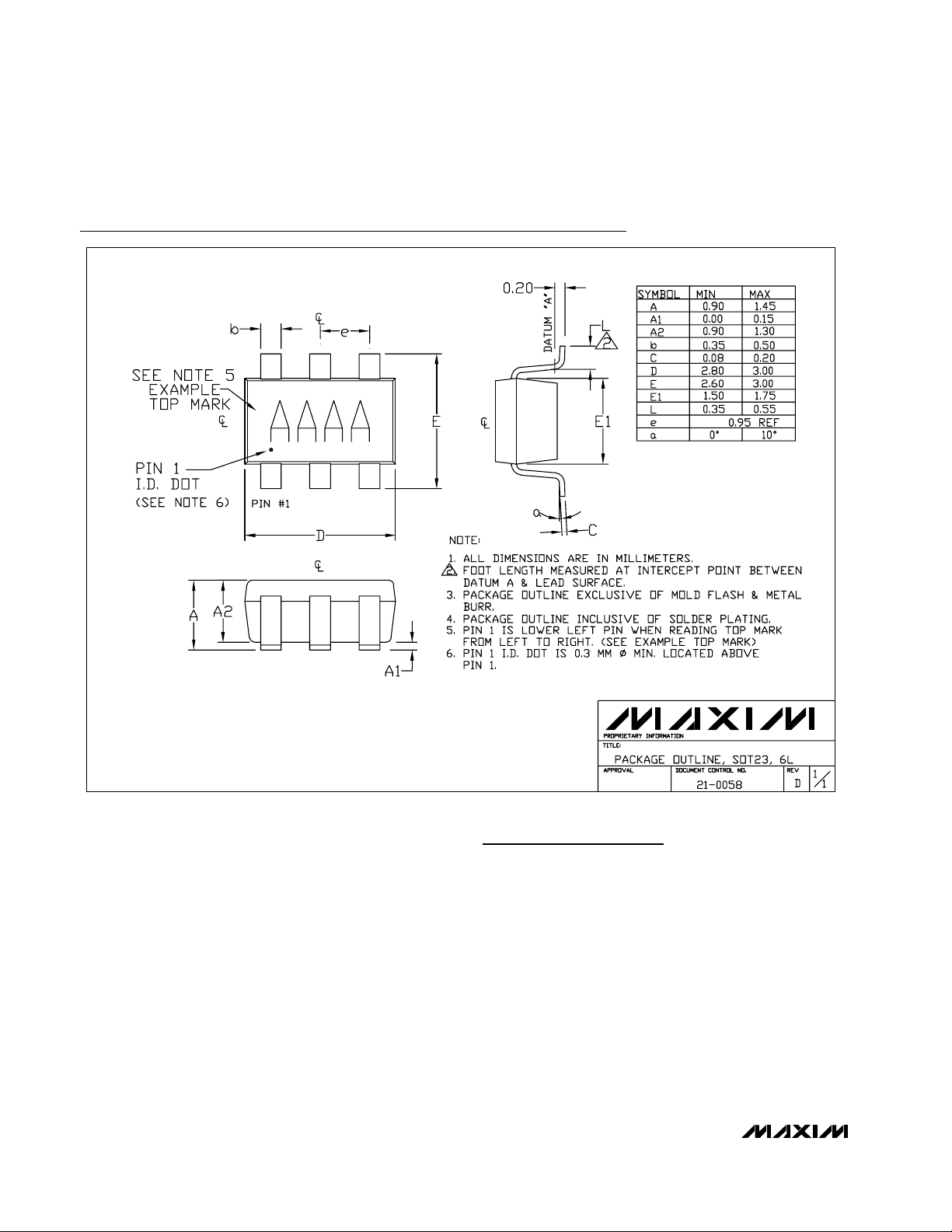
Package Information
6LSOT.EPS
Chip Information
TRANSISTOR COUNT: 109
 Loading...