

Page 1
For free samples & the latest literature: http://www.maxim-ic.com, or phone 1-800-998-8800.
For small orders, phone 1-800-835-8769.
General Description
The MAX2470/MAX2471 are flexible, low-cost, highreverse-isolation buffer amplifiers for applications with
discrete and module-based VCO designs. Both feature
differential 50Ω outputs for driving a single differential
(balanced) load or two separate single-ended (unbalanced) 50Ω loads. The MAX2470 offers a single-ended
input and has two selectable frequency ranges of operation: 10MHz to 500MHz and 10MHz to 200MHz. The
MAX2471 offers a differential input and operates from
10MHz to 500MHz. The MAX2470/MAX2471 also feature
high input impedance for maximum flexibility, enabling
them to be used with a variety of oscillator topologies.
High reverse isolation combined with low supply current
make them ideal for applications requiring high performance with low power.
These devices are also ideal for use as active baluns.
The MAX2470 converts a single-ended input to a differential output. The MAX2471 is useful as a differential
buffer stage or to convert from a differential input to two
single-ended outputs.
The MAX2470 operates from a single +2.7V to +5.5V
supply. At -5dBm output power, it consumes 5.5mA in
the high-frequency range and only 3.6mA in the
low-frequency range. The MAX2471 operates from a
+2.7V to +5.5V single supply and consumes 5.5mA.
Both devices are available in ultra-small SOT23-6 plastic packages, requiring minimal board space.
Applications
Cellular and PCS Mobile Phones
ISM-Band Applications
Active Baluns
General-Purpose Buffers/Amplifiers
Features
♦ +2.7V to +5.5V Supply Range
♦ Input Frequency Range
High: 10MHz to 500MHz (MAX2470/2471)
Low: 10MHz to 200MHz (MAX2470)
♦ >14dB Power Gain at 200MHz
♦ 64dB Typical Reverse Isolation at 200MHz
♦ Low-Distortion Output Drive
♦ Ultra-Small SOT23-6 Package
♦ High Input Impedance
♦ Single-Ended (MAX2470) or Differential
(MAX2471) Inputs
MAX2470/MAX2471
10MHz to 500MHz VCO Buffer Amplifiers
with Differential Outputs
________________________________________________________________
Maxim Integrated Products
1
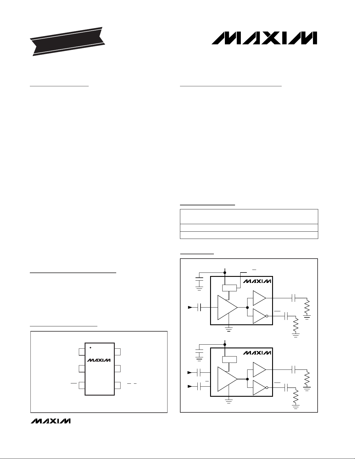
OUT
BIAS
V
CC
GND
OUT
50Ω
50Ω
IN
HI/LO
MAX2470
OUT
BIAS
V
CC
GND
OUT
50Ω
50Ω
IN
IN
MAX2471
Typical Operating Circuits
19-4797; Rev 0; 2/99
PART
MAX2470EUT-T
MAX2471EUT-T
-40°C to +85°C
-40°C to +85°C
TEMP. RANGE
PIN-
PACKAGE
6 SOT23-6
6 SOT23-6
EVALUATION KIT MANUAL
FOLLOWS DATA SHEET
Pin Configuration
Ordering Information
SOT TOP
MARK
AAAX
AAAY
16V
MAX2470
2
MAX2471
34
SOT23-6
5 IN
CC
HI/LO (IN)OUT
TOP VIEW
( ) ARE FOR MAX2471
OUT
GND
Page 2
f
OUT
= 200MHz,
RHI/LO = GND
No signal
MAX2470/MAX2471
10MHz to 500MHz VCO Buffer Amplifiers
with Differential Outputs
2 _______________________________________________________________________________________
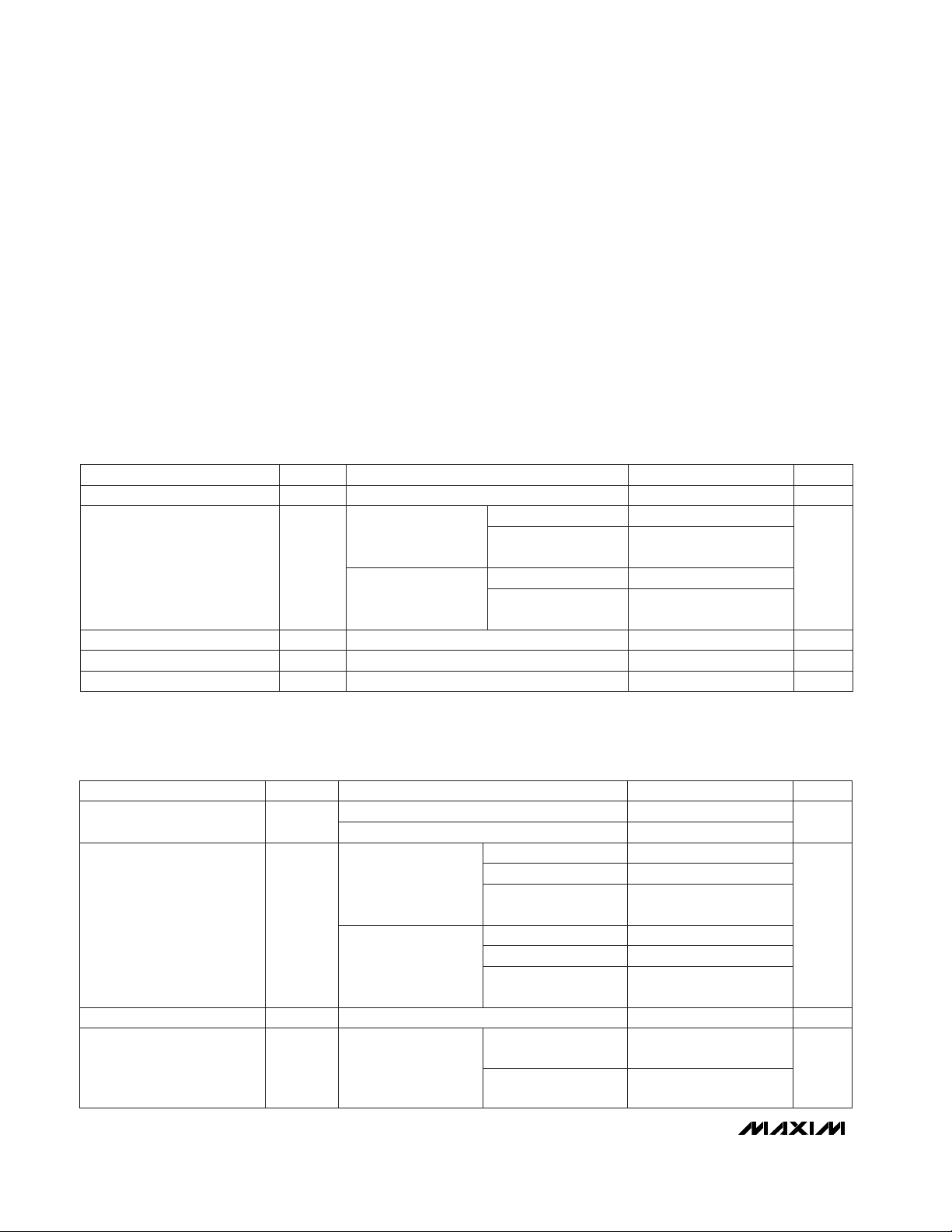
ABSOLUTE MAXIMUM RATINGS
DC ELECTRICAL CHARACTERISTICS
(Typical Operating Circuit, VCC= +2.7V to +5.5V, TA= T
MIN
to T
MAX
, unless otherwise noted. Typical values are at VCC= +3V,
T
A
= +25°C.) (Note 1)
AC ELECTRICAL CHARACTERISTICS—MAX2470
(VCC= +3V, HI/LO = VCC, all outputs are differentially measured between OUT and OUT driving a 50Ω load through a 180° hybrid,
T
A
= +25°C, unless otherwise noted.)
Stresses beyond those listed under “Absolute Maximum Ratings” may cause permanent damage to the device. These are stress ratings only, and functional
operation of the device at these or any other conditions beyond those indicated in the operational sections of the specifications is not implied. Exposure to
absolute maximum rating conditions for extended periods may affect device reliability.
VCCto GND..............................................................-0.3V to +7V
IN to GND......-0.3V to (V
CC
+ 0.3V) or 3.7V (whichever is lower)
IN to IN ..................................................................-2.2V to +2.2V
HI/LO to GND.............................................-0.3V to (V
CC
+ 0.3V)
Continuous Power Dissipation
SOT23-6 (derate 8.7mW/°C above +70°C)...................696mW
Operating Temperature Range ...........................-40°C to +85°C
Junction Temperature......................................................+150°C
Storage Temperature Range.............................-65°C to +150°C
Lead Temperature (soldering, 10sec )............................+300°C
VHI/LO = GND or V
CC
CONDITIONS
mA
5.1 7.4
V2.7 5.5V
CC
Supply Voltage Range
µA-10 10I
IN
HI/LO Input Bias Current
3.0 4.5
V2.0V
IH
HI/LO Input Level High
V0.6V
IL
HI/LO Input Level Low
UNITSMIN TYP MAXSYMBOLPARAMETER
HI/LO = V
CC
HI/LO = GND
HI/LO = V
CC
CONDITIONS
14.9
MHz
10 200
f
IN
10 500
Input Frequency Range
(Note 2)
14.9
13.8
14.1
UNITSMIN TYP MAXSYMBOLPARAMETER
HI/LO = V
CC
5.5
HI/LO = GND
3.6
I
CC
Supply Current
fIN= 10MHz, HI/LO = GND
R
SOURCE
= 50Ω
V/V16A
V
Voltage Gain (Note 4)
10.2
dB
10.2
NFNoise Figure
8.9 13.3 15.3
HI/LO = GND
dB
9.9 13.4 15.0
IS21I
2
Gain (Note 3)
No signal
P
OUT
= -5dBm,
R
LOAD
= 100Ω diff.
No signal
P
OUT
= -5dBm,
R
LOAD
= 100Ω diff.
fIN= 10MHz
fIN= 200MHz
fIN= 500MHz,
TA= T
MIN
to T
MAX
fIN= 10MHz
fIN= 200MHz
fIN= 200MHz,
TA= T
MIN
to T
MAX
f
OUT
= 500MHz,
HI/LO = V
CC
f
OUT
= 200MHz,
RHI/LO = GND
Page 3
MAX2470/MAX2471
10MHz to 500MHz VCO Buffer Amplifiers
with Differential Outputs
_______________________________________________________________________________________ 3
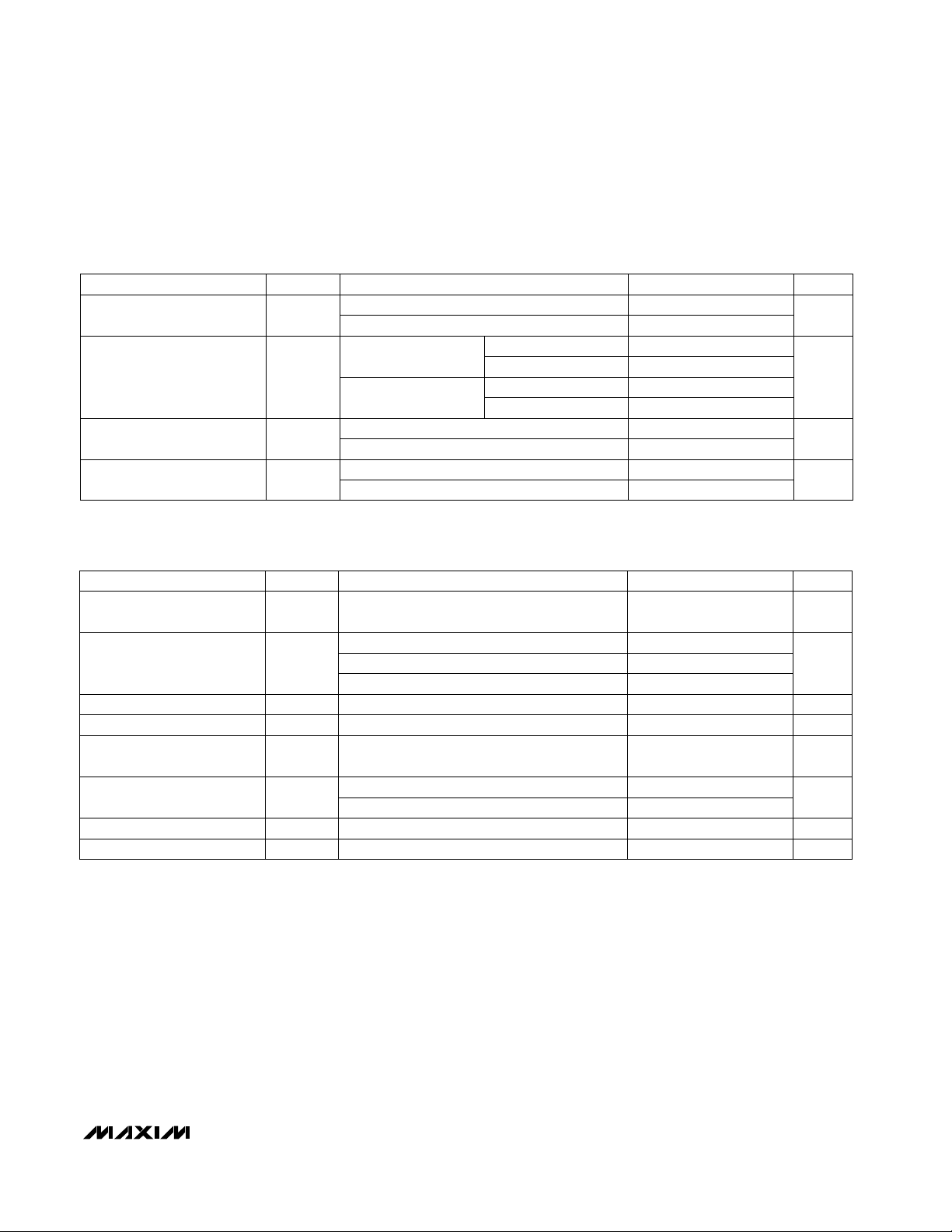
AC ELECTRICAL CHARACTERISTICS—MAX2471
(Typical values are measured at VCC= +3V, TA= +25°C, unless otherwise noted.) (Note 8)
AC ELECTRICAL CHARACTERISTICS—MAX2470 (continued)
(VCC= +3V, HI/LO = VCC, all outputs are differentially measured between OUT and OUT driving a 50Ω load through a 180° hybrid,
T
A
= +25°C, unless otherwise noted.)
Note 1: Limits are 100% production tested at T
A
= +25°C. Limits over the entire operating temperature range are guaranteed by
design and characterization but are not production tested.
Note 2: The part has been characterized over the specified frequency range. Operation outside of this range is possible but not
guaranteed.
Note 3: Gain specified for P
OUT
= -5dBm.
Note 4: Voltage gain measured with no input termination and no output load.
Note 5: Output VSWR is a single-ended measurement for each OUT and OUT.
Note 6: OUT to IN isolation with OUT terminated with 50Ω.
Note 7: Input terminated with 50Ω.
Note 8: Unless otherwise noted: all inputs are differentially measured between IN and IN driven by a 50Ω load through a 180°
hybrid; all outputs are differentially measured between OUT and OUT driving a 50Ω load through a 180° hybrid.
10MHz < f
OUT
< 500MHz, HI/LO = V
CC
1.5:1
CONDITIONS
10MHz < f
OUT
< 200MHz, HI/LO = GND
1.2:1
VSWR
OUT
Maximum Output VSWR
(OUT, OUT) (Note 5)
UNITSMIN TYP MAXSYMBOLPARAMETER
75
48
fIN= 500MHz, HI/LO = V
CC
37
75
fIN= 200MHz, HI/LO = GND
dB
45
Isolation OUT to OUT
(Note 7)
HI/LO = V
CC
dB
64
IS12I
2
Reverse Isolation
(Note 6)
fIN= 200MHz, P
OUT
= -5dBm, HI/LO = GND
dBc
-30
Harmonic Suppression
fIN= 500MHz, P
OUT
= -5dBm, HI/LO = V
CC
-26
fIN= 100MHz
fIN= 500MHz
fIN= 100MHz
fIN= 200MHz
HI/LO = GND
fIN= 10MHz
f
OUT
= 500MHz, R
SOURCE
= 50Ω
fIN= 10MHz
dBIS21I
2
Gain (Note 3)
V/V16A
V
Voltage Gain (Note 4)
8.4
fIN= 200MHz
CONDITIONS
fIN= 500MHz, TA= T
MIN
to T
MAX
11.3 15.6 17.8
15.9
MHz10 500f
IN
Input Frequency Range
(Note 2)
16.9
UNITSMIN TYP MAXSYMBOLPARAMETER
dBNFNoise Figure
10MHz < f
OUT
< 500MHz 1.5:1VSWR
OUT
Maximum Output VSWR
(OUT, OUT) (Note 5)
fIN= 100MHz 74
fIN= 500MHz 57
dBIS12I
2
Reverse Isolation
fIN= 500MHz 35 dB
Isolation OUT to OUT (Note 7)
fIN= 500MHz, P
OUT
= -5dBm -29 dBcHarmonic Suppression
Page 4

MAX2470/MAX2471
10MHz to 500MHz VCO Buffer Amplifiers
with Differential Outputs
4 _______________________________________________________________________________________
Typical Operating Characteristics
(VCC= +3.0V, MAX2470 output and MAX2471 input and output measurements taken differentially, TA= +25°C, unless otherwise
noted.)
3.2
3.3
3.4
3.5
3.6
3.7
3.8
3.9
4.0
2.5 3.53.0 4.0 4.5 5.0 5.5
MAX2470
SUPPLY CURRENT vs. SUPPLY VOLTAGE
(HI/LO = GND)
MAX2470/71-01
SUPPLY VOLTAGE (V)
SUPPLY CURRENT (mA)
-5dBm OUTPUT POWER
f
IN
= 200MHz
HI/LO = GND
TA = +85°C
TA = +25°C
TA = -40°C
4.8
5.0
4.9
5.1
5.3
5.2
5.4
5.5
5.6
5.7
5.8
5.9
6.0
2.5 3.53.0 4.0 4.5 5.0 5.5
MAX2470 (HI/LO = VCC) AND MAX2471
SUPPLY CURRENT vs. SUPPLY VOLTAGE
MAX2470/71-02
SUPPLY VOLTAGE (V)
SUPPLY CURRENT (mA)
TA = +25°C
-5dBm OUTPUT POWER
f
IN
= 500MHz
HI/LO = GND (MAX2470)
TA = -40°C
TA = +85°C
-16
-13
-14
-15
-12
-9
-10
-11
-8
-7
-5
-6
-4
-3
-1
-2
0
-30 -24-26-28 -20-22 -16-18 -12-14 -10
MAX2470
OUTPUT POWER vs. INPUT POWER
MAX2470/71-03
INPUT POWER (dBm)
OUTPUT POWER (dBm)
HI/LO = GND
f
IN
= 200MHz
HI/LO = V
CC
fIN = 500MHz
8.0
10.0
9.0
14.0
13.0
12.0
11.0
15.0
16.0
0 10050 150 200
MAX2470/71-04
FREQUENCY (MHz)
IS
21
I
2
(dB)
TA = -40°C
HI/LO = GND
MAX2470
TRANSDUCER GAIN vs. FREQUENCY
(HI/LO = GND)
TA = +25°C
TA = +85°C
10.0
11.0
10.5
11.5
12.0
0 200 300100 400 500
MAX2470
NOISE FIGURE vs. FREQUENCY
(HI/LO = V
CC
)
MAX2470/71-07
FREQUENCY (MHz)
NOISE FIGURE (dB)
HI/LO = V
CC
9.0
10.0
14.0
13.0
12.0
11.0
15.0
17.0
16.0
0 200100 300 400 500
MAX2470
TRANSDUCER GAIN vs. FREQUENCY
(HI/LO = V
CC
)
MAX2470/71-05
FREQUENCY (MHz)
IS
21
I
2
(dB)
TA = +85°C
TA = +25°C
TA = -40°C
HI/LO = V
CC
9.5
10.0
11.0
10.5
11.5
12.0
0 10050
150
200
MAX2470
NOISE FIGURE vs. FREQUENCY
(HI/LO = GND)
MAX2470/71-06
FREQUENCY (MHz)
NOISE FIGURE (dB)
HI/LO = GND
10,000
1
0 150 20050 100 350 500
MAX2470
REAL INPUT IMPEDANCE vs. FREQUENCY
10
100
1000
MAX2470/71-08
FREQUENCY (MHz)
RE [Z
IN
] (Ω)
250 300 450400
HI/LO = V
CC
-3000
-2000
-2500
-1000
-1500
-500
0
0 200100 300 400 500
MAX2470
IMAGINARY INPUT IMPEDANCE vs. FREQUENCY
MAX2470/71-09
FREQUENCY (MHz)
IM [Z
IN
] (Ω)
HI/LO = V
CC
Page 5

MAX2470/MAX2471
10MHz to 500MHz VCO Buffer Amplifiers
with Differential Outputs
_______________________________________________________________________________________
5
1.00
1.25
1.50
0 200100 300 400 500
MAX2470
OUTPUT VSWR vs. FREQUENCY
MAX2470/71-10
FREQUENCY (MHz)
OUTPUT VSWR
HI/LO = V
CC
INPUT TERMINATED IN 50Ω
SINGLE-ENDED MEASUREMENT
OUT
OUT
20
40
30
70
60
50
80
90
0 200100 300 400 500
MAX2470
OUTPUT ISOLATION vs. FREQUENCY
MAX2470/71-11
FREQUENCY (MHz)
OUTPUT ISOLATION (dB)
HI/LO = V
CC
SINGLE-ENDED
MEASUREMENT
OUT TO IN
OUT TO IN
OUT TO OUT
INPUT TERMINATED IN 50Ω
-14
-12
-10
-8
-6
-4
-2
0
2
-30 -24 -22-28 -26 -20 -18 -16 -14 -12 -10
MAX2471
OUTPUT POWER vs. INPUT POWER
MAX2470/71-12
INPUT POWER (dBm)
OUTPUT POWER (dBm)
fIN = 200MHz
fIN = 500MHz
Typical Operating Characteristics (continued)
(VCC= +3.0V, MAX2470 output and MAX2471 input and output measurements taken differentially, TA= +25°C unless otherwise
noted.)
14.0
14.5
15.0
15.5
16.0
16.5
17.0
17.5
0 150 20050 100 250 300 350 400 450 500
MAX2471
DIFFERENTIAL TRANSDUCER
POWER GAIN vs. FREQUENCY
MAX2470/71-13
FREQUENCY (MHz)
TRANSDUCER POWER GAIN (dB)
TA = +25°C
TA = +85°C
TA = -40°C
7.25
7.50
7.75
8.00
8.25
8.50
0 150 20050 100 250 300 350 400 450 500
MAX2471
NOISE FIGURE vs. FREQUENCY
MAX2470/71-14
FREQUENCY (MHz)
NOISE FIGURE (dB)
1
10
100
1000
10,000
0 150 20050 100 250 300 350 400 450 500
MAX2471
REAL INPUT IMPEDANCE vs. FREQUENCY
MAX2470/71-15
FREQUENCY (MHz)
RE [Z
IN
] (Ω)
-1000
-500
0
500
0 200100 300 400 500
MAX2471
IMAGINARY INPUT IMPEDANCE
vs. FREQUENCY
MAX2470/71-16
FREQUENCY (MHz)
IM [Z
IN
] (Ω)
1.00
1.25
1.50
0 200100 300 400 500
MAX2471
OUTPUT VSWR vs. FREQUENCY
MAX2470/71-17
FREQUENCY (MHz)
OUTPUT VSWR
INPUT TERMINATED
SINGLE-ENDED MEASUREMENT
VSWR OUT
VSWR OUT
20
30
60
50
40
80
70
90
0 200 300100 400 500
MAX2471
OUTPUT ISOLATION vs. FREQUENCY
MAX2470/71-18
FREQUENCY (MHz)
OUTPUT ISOLATION (dB)
OUT TO IN
INPUT TERMINATED IN 50Ω
OUT TO OUT
SINGLE-ENDED
MEASUREMENT
Page 6

_______________ Detailed Description
Bandwidth Control Circuitry
The MAX2470 features a logic-controlled bias circuit
which optimizes the performance for input frequencies
from 10MHz to 500MHz (HI/LO = VCC) and 10MHz to
200MHz (HI/LO = GND). Operating with HI/LO = GND
significantly reduces power consumption.
__________ Applications Information
Input Considerations
The MAX2470/MAX2471 offer high-impedance inputs,
ideal for low-distortion buffering of a VCO. For applications with discrete transistor-based oscillator designs,
simply AC-couple the oscillator directly to the inputs.
The buffer’s high input impedance results in minimal
loading on the oscillator. For still higher real input
impedance and reduced loading effects, match the
inputs with a shunt-L matching circuit followed by a
series blocking capacitor. For use with 50Ω VCO modules, terminate the buffer input(s) with a 50Ω shunt
resistor followed by a series-blocking capacitor. This
provides a very stable 50Ω termination and increases
reverse isolation. For those applications needing both
high gain and good input match, reactively match the
buffer inputs to 50Ω with simple two-element matching
circuits followed by a series blocking capacitor.
Output Considerations
The MAX2470 and MAX2471 incorporate fully differential output stages capable of driving an AC-coupled
100Ω differential load or two AC-coupled 50Ω singleended loads. This is ideal for applications that require
the oscillator to drive two application circuits (e.g. mixer
and PLL) simultaneously. The high output-to-output isolation ensures minimal interaction between multiple
load circuits.
Layout and Power-Supply Bypassing
A properly designed PC board is essential to any RF/
microwave circuit. Be sure to use controlled impedance
lines on all high-frequency inputs and outputs. Bypass
the power supply with decoupling capacitors as close to
the VCCpins as possible. For long VCClines (inductive), it
may be necessary to add additional decoupling capacitors located further away from the device package.
Proper grounding of GND is essential. If the PC board
uses a topside RF ground, connect GND directly to it.
For a board where the ground plane is not on the component side, the best technique is to connect GND to
the board with a plated through-hole (via) to the ground
plane close to the package.
MAX2470/MAX2471
10MHz to 500MHz VCO Buffer Amplifiers
with Differential Outputs
6 _______________________________________________________________________________________
Pin Description
Differential Noninverting Buffer Output. Broadband 50Ω output. AC coupling is required.
Do not DC couple to this pin.
OUT1
PIN
1
MAX2471MAX2470
NAME
2
RF Ground. Connect to the ground plane as close as possible to the IC to minimize
ground path inductance.
GND2
3
—
Bias and Bandwidth Control Input. Connect to VCCto set internal bias for higher bandwidth operation (10MHz to 500MHz). Connect to GND to set internal bias for lower bandwidth operation (10MHz to 200MHz) and to reduce overall current consumption.
HI/LO
4
Differential Inverting Buffer Output. Broadband 50Ω output. AC coupling is required. Do
not DC couple to this pin.
OUT
3
4
Differential Inverting Buffer Input. High impedance input to buffer amplifier. See
Setting
The Input Impedance
section.
IN
—
5
6 Supply Voltage Input. +2.7V < VCC< +5.5V.V
CC
6
Differential Noninverting Buffer Input. High impedance to buffer amplifier. See
Setting The
Input Impedance
section.
IN5
FUNCTION
Page 7

MAX2470/MAX2471
10MHz to 500MHz VCO Buffer Amplifiers
with Differential Outputs
_______________________________________________________________________________________ 7
Chip Information
TRANSISTOR COUNT: 67
Package Information
6LSOT.EPS
Page 8

MAX2470/MAX2471
10MHz to 500MHz VCO Buffer Amplifiers
with Differential Outputs
8 _______________________________________________________________________________________
NOTES
 Loading...