

_______________General Description
The monolithic MAX2452 is a quadrature modulator
with supporting oscillator and divide-by-8 prescaler. It
operates from a single +3V supply and draws only
4.1mA. The modulator accepts differential I and Q
baseband signals with amplitudes up to 1.35Vp-p and
bandwidths up to 15MHz. It produces a differential output up to 80MHz.
Pulling the CMOS-compatible ENABLE pin low reduces
the supply current to 2µA. To minimize spurious feedback, the MAX2452’s internal oscillator is set at twice
the IF via external tuning components. The oscillator
and associated phase shifters produce differential signals exhibiting low amplitude and phase imbalance,
yielding 42dB sideband rejection. The MAX2452 comes
in a 16-pin narrow SO package.
________________________Applications
Digital Cordless Phones
GSM and North American Cellular Phones
Wireless LANs
Digital Communications
Two-Way Pagers
____________________________Features
♦ IF Output Frequency up to 80MHz
♦ Input Bandwidth up to 15MHz
♦ On-Chip Oscillator with External Tuning Circuit
♦ On-Chip Divide-by-8 Prescaler
♦ Integrated Quadrature Phase Shifters
♦ Self-Biased Differential Baseband Inputs
♦ CMOS-Compatible Enable
♦ 4.1mA Operating Supply Current
2µA Shutdown Supply Current
MAX2452
3V, Ultra-Low-Power
Quadrature Modulator
________________________________________________________________
Maxim Integrated Products
1
16
15
14
13
12
11
10
9
1
2
3
4
5
6
7
8
IF
GND
V
CC
N.C.
PRE_OUT
LO_V
CC
LO_GND
TANK
IF
GND
I
I
Q
Q
ENABLE
TANK
TOP VIEW
MAX2452
SO
MAX2452
MODULATOR
LOCAL
OSCILLATOR
÷2
÷2 ÷4
QUADRATURE
PHASE
GENERATOR
90°
0°
Σ
LO_V
CC
TANK
TANK
LO_GND
I
I
Q
Q
V
CC
PRE_OUT
IF
IF
BANDGAP BIAS
GND ENABLE
PRESCALER
11
8
9
10
3
4
5
6
14
12
16
1
72, 15
MASTER BIAS
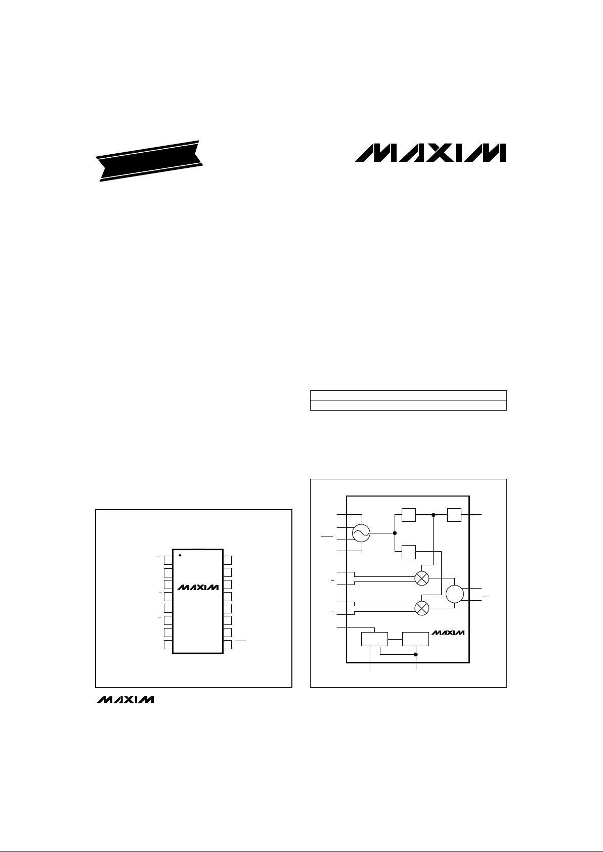
__________________Pin Configuration
________________Functional Diagram
Call toll free 1-800-998-8800 for free samples or literature.
PART
MAX2452ISE* -20°C to +85°C
TEMP. RANGE PIN-PACKAGE
16 Narrow SO
EVALUATION KIT
AVAILABLE
______________Ordering Information
19-0425; Rev 1; 9/95
* An alternate marking, MAX2452CSE, has been identically tested.
MAX2452
3V, Ultra-Low-Power
Quadrature Modulator
2 _______________________________________________________________________________________
ABSOLUTE MAXIMUM RATINGS
DC ELECTRICAL CHARACTERISTICS
(VCC= LO_VCC= 2.7V to 3.3V, TA= -20°C to +85°C, unless otherwise noted.)
AC ELECTRICAL CHARACTERISTICS
(VCC= LO_VCC= 3.0V, f
OSC
= 140MHz, ENABLE = 2.6V, fII= fQQ= 600kHz, TA= -20°C to +85°C, unless otherwise noted.)
Stresses beyond those listed under “Absolute Maximum Ratings” may cause permanent damage to the device. These are stress ratings only, and functional
operation of the device at these or any other conditions beyond those indicated in the operational sections of the specifications is not implied. Exposure to
absolute maximum rating conditions for extended periods may affect device reliability.
Note 1: Guaranteed by design, not tested.
Note 2: The frequency range can be extended in either direction, but has not been characterized. At higher frequencies, the IF
output level may decrease and distortions may increase.
V
CC
, LO_VCCto GND............................................-0.3V to +4.5V
ENABLE, TANK, TANK
, I, I, Q, Q to GND..................VCC+ 0.3V
Continuous Power Dissipation (T
A
= +70°C)
SO (derate 8.33mW/°C above +70°C)..........................667mW
Operating Temperature Range ...........................-20°C to +85°C
Storage Temperature Range ............................–65°C to +165°C
Lead Temperature (soldering, 10sec).............................+300°C
Enable = 0.4V
Enable = VCC- 0.4V
Enable = VCC- 0.4V
CONDITIONS
kΩ35 44ZII, Z
QQ
Differential Input Impedance
V1.25 1.5 1.75VI, VI, VQ, V
Q
I, I, Q, Q Voltage Level
µA220I
CC OFF
Shutdown Supply Current
mA4.1 7I
CC ON
V2.7 3.3VCC, LO_V
CC
Supply Voltage Range
Supply Current
VLO_VCC- 1.1 LO_VCC- 0.8V
TANK
TANK Voltage Level
VLO_VCC- 1.1 LO_VCC- 0.8V
TANK
TANK Voltage Level
VVCC- 1.7 VCC- 1.35V
IF
IF Voltage Level
VVCC- 1.7 VCC- 1.35V
IF
IF Voltage Level
µs10t
ON/OFF
Enable/Disable Time
µA110I
EN
ENABLE Bias Current
V0.4V
ENL
ENABLE Low Voltage
VVCC- 0.4V
ENH
ENABLE High Voltage
UNITSMIN TYP MAXSYMBOLPARAMETER
RL= 10kΩ, CL< 6pF, rising edge,
TA= +25°C
RL= 10kΩ, CL< 6pF
(Notes 1, 2)
VII= VQQ= 1.2Vp-p
VII= VQQ= 1.2Vp-p, RL= 200kΩ
differential, CL< 5pF differential
(Note 1)
(Note 1)
CONDITIONS
V/µs60SR
PRE_OUT
PRE_OUT Slew Rate
Vp-p0.35V
PRE_OUT
PRE_OUT Output Voltage
MHz70 140 160f
OSC
Oscillator Frequency Range
dBc-36LO Leakage at Output
dB42Sideband Rejection
degrees<±3I/Q Phase Match
dB<±0.3I/Q Amplitude Match
mVp-p65V
IFIFp-p
IF Differential Output Voltage
MHz15BW
IQ
I and Q Signal Bandwidth
Vp-p1.2 1.35V
IIp-p
, V
QQp-p
Differential Input Voltage
UNITSMIN TYP MAXSYMBOLPARAMETER
MAX2452
3V, Ultra-Low-Power
Quadrature Modulator
_______________________________________________________________________________________
3
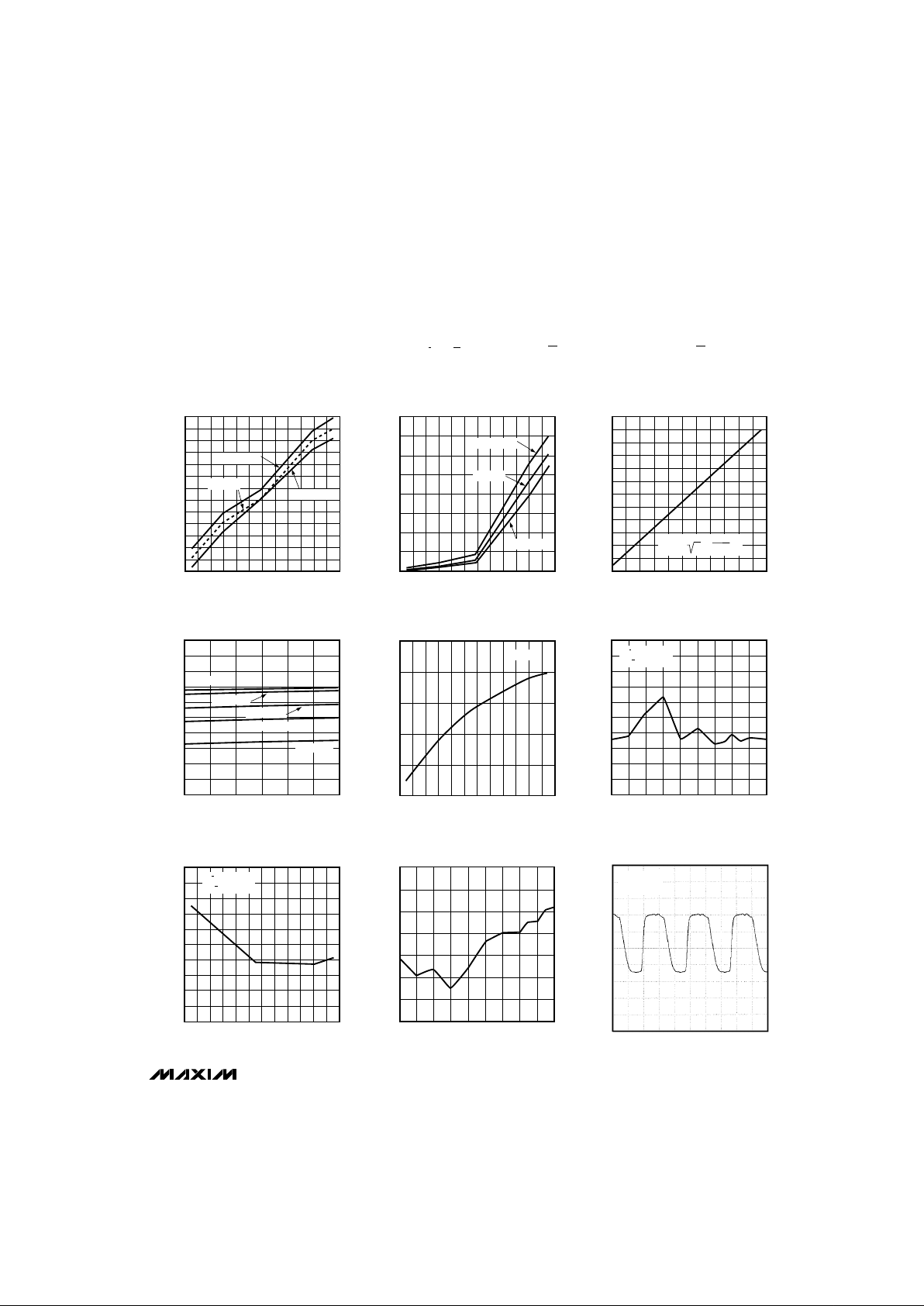
4.8
4.7
4.6
4.5
4.4
4.3
4.2
4.1
4.0
3.9
3.8
3.7
3.6
3.5
-30 -10 10 30 50 70 90
MAX2452-01
TEMPERATURE (°C)
SUPPLY CURRENT (mA)
SUPPLY CURRENT
vs. TEMPERATURE
V
CC
= 2.7V
V
CC
= 3.3V
V
CC
= 3V
0
2
4
6
8
10
12
14
16
-30 -10 10 30 50 70 90
MAX2452-02
TEMPERATURE (°C)
V
CC
= 2.7V
V
CC
= 3.3V
V
CC
= 3V
SHUTDOWN SUPPLY CURRENT
vs. TEMPERATURE
SUPPLY CURRENT (µA)
-30
-34
-38
-42
-46
-50
-54
-26 -22 -18 -14 -10 -6
MAX2452-03
BASEBAND INPUT (dBV
RMS
)
OUTPUT (dBV
RMS
)
IF OUTPUT
vs. BASEBAND INPUT
Vp-p = 2 2 x 10 (V)
dBV
RMS
20
54
56
58
60
62
64
66
68
70
72
74
2.7
MAX2452-04
VCC (V)
IF OUTPUT (mVp-p)
2.8 2.9 3.0 3.1 3.2 3.3
TA = +85°C
TA = +70°C
TA = +25°C
TA = 0°C
TA = -25°C
IF OUTPUT
vs. SUPPLY VOLTAGE
-50
-48
-46
-44
-42
-40
-38
-36
-34
-32
-30
-30 -10 10 30 50 70 90
MAX2452-07
TEMPERATURE (°C)
SIDEBAND REJECTION (dBc)
V
II
= 1.2Vp-p
V
QQ
= 1.2Vp-p
SIDEBAND REJECTION
vs. TEMPERATURE
70
68
66
64
62
60
-30 -10 10 30 50 70 90
MAX2452-05
TEMPERATURE (°C)
IF OUTPUT (mVp-p)
V
CC
= 3V
IF OUTPUT
vs. TEMPERATURE
-50
-48
-46
-44
-42
-40
-38
-36
-34
-32
-30
35 40 45 50 55 60 65 70 75 80
MAX2452-06
IF FREQUENCY (MHz)
SIDEBAND REJECTION (dBc)
V
II
= 1.2Vp-p
V
QQ
= 1.2Vp-p
SIDEBAND REJECTION
vs. IF FREQUENCY
-30
-32
-34
-36
-38
-40
-42
-44
8035 40 45 50 55 60 65 70 75
MAX2452-08
IF FREQUENCY (MHz)
LO LEAKAGE (dBc)
LO LEAKAGE
vs. IF FREQUENCY
__________________________________________Typical Operating Characteristics
(VCC= LO_VCC= 3.0V, f
OSC
= 140MHz, ENABLE = 2.6V, fII= fQQ= 600kHz, RL(IF, IF) = 200kΩ differential, CL(IF, IF) < 5pF
differential, TA= +25°C, unless otherwise noted.)
100mV/
div
PRE_OUT WAVEFORM
MAX2452-09
20ns/div
RL = 10kΩ
C
L
< 6pF

MAX2452
3V, Ultra-Low-Power
Quadrature Modulator
4 _______________________________________________________________________________________
-60
69.0 70.6
71.0
MODULATOR OUTPUT SPECTRUM
-50
0
MAX2453-10
(MHz)
(dBc)
69.4 70.0
-20
-10
-30
-40
VII = 1.2Vp-p
V
QQ
= 1.2Vp-p
____________________________Typical Operating Characteristics (continued)
(VCC= LO_VCC= 3.0V, f
OSC
= 140MHz, ENABLE = 2.6V, fII= fQQ= 600kHz, RL(IF, IF) = 200kΩ differential, CL(IF, IF) < 5pF
differential, TA= +25°C, unless otherwise noted.)
NAME FUNCTION
1 IF IF Inverting Output
2, 15 GND Ground
PIN
3 I Inphase Input
4 I Inphase Inverting Input
8 TANK
Local-Oscillator Resonant Tank
Input
7 ENABLE Enable Control, active high
6 Q Quadrature Inverting Input
5 Q Quadrature Input
13 N.C.
No Connect, no internal connection
to this pin
12 PRE_OUT
Local-Oscillator Divide-by-8
Prescaled Output
11 LO_V
CC
Local-Oscillator Supply
10 LO_GND Local-Oscillator Ground
9 TANK
Local-Oscillator Resonant Tank
Inverting Input
_____________________Pin Description
16 IF IF Output
14 V
CC
Modulator Supply

MAX2452
3V, Ultra-Low-Power
Quadrature Modulator
_______________________________________________________________________________________ 5
_______________Detailed Description
The MAX2452 quadrature modulator integrates several
important RF functions on a single chip. It includes differential buffers for the baseband inputs, two doublebalanced mixers, a local oscillator, a quadrature phase
generator, and a divide-by-8 prescaler. The prescaler
simplifies the implementation of a phase-locked loop.
Each of the functional blocks (shown in the
Functional
Diagram
) is described in detail in the following sec-
tions.
Local Oscillator
The local-oscillator section is formed by an emitter-coupled differential pair. Figure 1 shows the equivalent
local-oscillator circuit schematic. An external LC resonant tank determines the oscillation frequency, and the
Q of this resonant tank determines the phase noise of
the oscillator. The oscillation frequency is twice the IF
frequency, so that the quadrature phase generator can
use two latches to generate precise quadrature signals.
Quadrature Phase Generator
The quadrature phase generator uses two latches to
divide the local-oscillator frequency by two, and generates two precise quadrature signals. Internal limiting
amplifiers shape the signals to approximate square
waves to drive the Gilbert-cell mixers in the modulator.
The inphase signal (at half the local-oscillator frequency) is further divided by four for an external phaselocked loop.
Modulator
The modulator accepts up to 1.35Vp-p I and Q differential baseband signals up to 15MHz, and upconverts
them to higher-frequency IF signals. Since these inputs
are biased internally at around 1.5V, you can improve
carrier suppression by externally capacitively coupling
the signals into these high-impedance ports (the differential input impedance is approximately 44kΩ). The
self-bias design is for very low on-chip offset, resulting
in excellent carrier suppression. The IF output is
designed to drive a high impedance (>20kΩ), such as
an IF buffer or an upconverter mixer.
Prescaler
The prescaler output, PRE_OUT, is buffered and
swings typically 0.35Vp-p with a 10kΩ and 6pF load. It
can be AC-coupled to the input of a frequency synthesizer.
Master Bias
During normal operation, ENABLE should remain above
VCC- 0.4V. Pulling the ENABLE input low shuts off the
master bias and reduces the circuit current to 2µA. The
master bias section includes a bandgap reference
generator and a PTAT (Proportional To Absolute
Temperature) current generator.
TANK TANK
Q1 Q2
Q3 Q4
R
L
5k
R
L
5k
L0_V
CC
TO
DIVIDE-BY-2
Figure 1. Local-Oscillator Equivalent Circuit

MAX2452
3V, Ultra-Low-Power
Quadrature Modulator
6 _______________________________________________________________________________________
Applications Information
The MAX2452 quadrature modulator is designed to
upconvert I and Q baseband signals to IF frequencies
up to 80MHz. Figure 2 shows a typical application
block diagram, in which the MAX2452 is used for the
first upconversion in a dual-conversion transmitter.
Figure 3 shows an implementation of a resonant tank
circuit. The inductor, two capacitors, and a dual varactor form the resonant circuit of the oscillator. The frequency range of the oscillator shown in Figure 3 is
130MHz to 160MHz. The inductor is directly connected
across the local oscillator’s tank ports so that it will not
lock up the oscillator in a stable state during start-up.
The two 33pF capacitors increase the Q of the resonant
circuit and reduce the VCO gain. They can be changed
to meet individual applications requirements. The oscillation frequency can be determined using the following
formula:
C
STRAY
, L
STRAY
: parasitic capacitance and induc-
tance.
To alter the oscillation frequency range, change the
inductance, the capacitance, or both. Make sure the Q
of the resonant tank does not drop below 35.
where REQ= 10kΩ (see Figure 1).
The oscillation frequency can be changed by altering
the control voltage, V
CTRL
.
MAX2452
DSP
PROCESSING
0°
I
Q
÷8
90°
UP CONVERTER
Σ
Figure 2. Typical Application Block Diagram
C1 = 33pF
10k
0.1µF
1/2KV1410
1/2KV1410
L = 100nH
47k
47kC2 = 33pF
TANK
TANK
V
CTRL
Figure 3. Typical Resonant Tank Circuit
f
LC
where
C
CC C
C
and
LLL
o
EQ EQ
EQ
VAR
STRAY
EQ STRAY
=
=
++
+
=+
1
2
1
11122
π
QR
C
L
EQ
EQ
EQ
=

MAX2452
3V, Ultra-Low-Power
Quadrature Modulator
_______________________________________________________________________________________ 7
________________________________________________________Package Information
DIM
A
A1
B
C
E
e
H
L
MIN
0.053
0.004
0.014
0.007
0.150
0.228
0.016
MAX
0.069
0.010
0.019
0.010
0.157
0.244
0.050
MIN
1.35
0.10
0.35
0.19
3.80
5.80
0.40
MAX
1.75
0.25
0.49
0.25
4.00
6.20
1.27
INCHES MILLIMETERS
21-0041A
Narrow SO
SMALL-OUTLINE
PACKAGE
(0.150 in.)
DIM
D
D
D
MIN
0.189
0.337
0.386
MAX
0.197
0.344
0.394
MIN
4.80
8.55
9.80
MAX
5.00
8.75
10.00
INCHES MILLIMETERS
PINS
8
14
16
1.270.050
L
0°-8°
HE
D
e
A
A1
C
0.101mm
0.004in.
B

Maxim cannot assume responsibility for use of any circuitry other than circuitry entirely embodied in a Maxim product. No circuit patent licenses are
implied. Maxim reserves the right to change the circuitry and specifications without notice at any time.
8
___________________Maxim Integrated Products, 120 San Gabriel Drive, Sunnyvale, CA 94086 (408) 737-7600
© 1995 Maxim Integrated Products Printed USA is a registered trademark of Maxim Integrated Products.
MAX2452
3V, Ultra-Low-Power
Quadrature Modulator
Maxim cannot assume responsibility for use of any circuitry other than circuitry entirely embodied in a Maxim product. No circuit patent licenses are
implied. Maxim reserves the right to change the circuitry and specifications without notice at any time.
8
___________________Maxim Integrated Products, 120 San Gabriel Drive, Sunnyvale, CA 94086 (408) 737-7600
© 1995 Maxim Integrated Products Printed USA is a registered trademark of Maxim Integrated Products.
 Loading...