

19-0493; Rev 0; 12/95
EVALUATION KIT
AVAILABLE
3V, Ultra-Low-Power
Quadrature Demodulator
_______________General Description
The monolithic MAX2451 is a quadrature demodulator
with a supporting oscillator and divide-by-8 prescaler. It
operates from a single +3V supply and draws only
5.5mA. The demodulator accepts an amplified and filtered IF signal in the 35MHz to 80MHz range, and
demodulates it into I and Q baseband signals with
51dB of voltage conversion gain. The IF input is terminated with a 400Ω thin-film resistor for matching to an
external IF filter. The baseband outputs are fully differential and have 1.2Vp-p signal swings.
Pulling the CMOS-compatible ENABLE pin low shuts
down the MAX2451 and reduces the supply current to
less than 2µA, typical. To minimize spurious feedback,
the MAX2451’s internal oscillator is set at twice the IF
frequency via external tuning components. The
MAX2451 comes in a 16-pin narrow SO package.
________________________Applications
Digital Cordless Phones
GSM and North American Cellular Phones
Wireless LANs
Digital Communications
Pagers
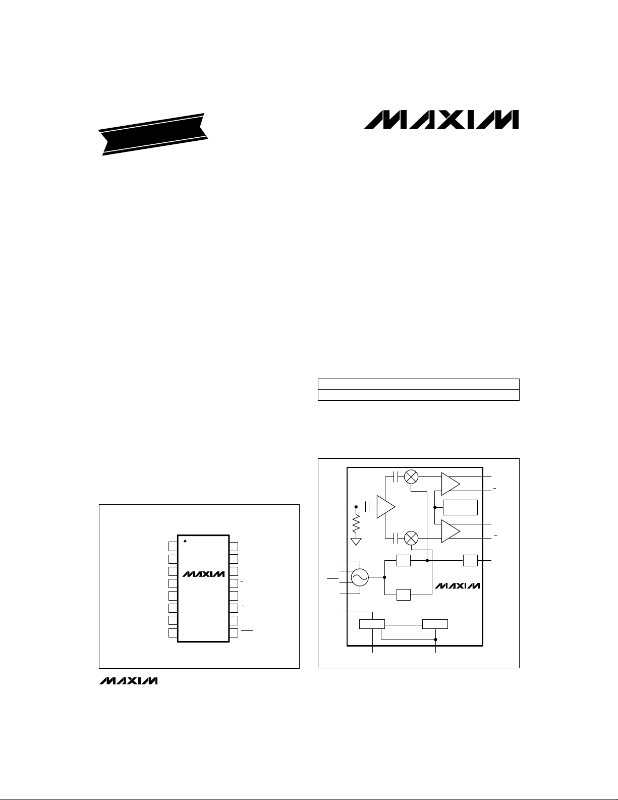
__________________Pin Configuration
TOP VIEW
IF
GND
GND
N.C.
ENABLE
PRE_OUT
LO_V
TANK
1
2
3
MAX2451
4
5
6
7
CC
8
SO
16
15
14
13
12
11
10
9
GND
V
CC
I
I
Q
Q
LO_GND
TANK
____________________________Features
♦ Integrated Quadrature Phase Shifters
♦ On-Chip Oscillator (Requires External Tuning
Circuit)
♦ 51dB Voltage Conversion Gain
♦ On-Chip Divide-by-8 Prescaler
♦ Baseband Output Bandwidth Up to 9MHz
♦ CMOS-Compatible Enable
♦ 5.5mA Operating Supply Current
2µA Shutdown Supply Current
______________Ordering Information
PART
MAX2451CSE 0°C to +70°C
TEMP. RANGE PIN-PACKAGE
16 Narrow SO
________________Functional Diagram
14
I
13
12
11
6
I
Q
Q
PRE_OUT
LO_V
TANK
TANK
LO_GND
V
1
IF
400Ω
7
CC
8
9
10
LOCAL
OSCILLATOR
15
CC
BANDGAP BIAS
DEMODULATOR
0°
÷ 2 ÷ 4
QUADRATURE
PHASE
GENERATOR
÷ 2
MASTER BIAS
PRESCALER
90°
52, 3, 16
ENABLEGND
BIAS
MAX2451
MAX2451
________________________________________________________________
Maxim Integrated Products
Call toll free 1-800-998-8800, or visit our WWW site at http://www.maxim-ic.com
for free samples or the latest literature.
1
3V, Ultra-Low-Power
Quadrature Demodulator
ABSOLUTE MAXIMUM RATINGS
VCC, LO_VCCto GND............................................-0.3V to +4.5V
ENABLE, TANK, TANK
to GND.............................................-0.3V to (VCC+ 0.3V)
Q, Q
IF to GND...............................................................-0.3V to +1.5V
Stresses beyond those listed under “Absolute Maximum Ratings” may cause permanent damage to the device. These are stress ratings only, and functional
operation of the device at these or any other conditions beyond those indicated in the operational sections of the specifications is not implied. Exposure to
absolute maximum rating conditions for extended periods may affect device reliability.
MAX2451
, I, I,
DC ELECTRICAL CHARACTERISTICS
(VCC= LO_VCC= TANK = +2.7V to +3.3V, ENABLE = VCC- 0.4V, GND = LO_GND = 0V, I = I = Q = Q = IF = TANK = OPEN,
= 0°C to +70°C, unless otherwise noted.)
T
A
Supply Voltage Range
Supply Current
Shutdown Supply Current
Enable/Disable Time
ENABLE Bias Current
ENABLE High Voltage
ENABLE Low Voltage
IF Input Impedance
I, I, Q, Q Voltage Level
VCC,
LO_V
CC(ON)
CC(OFF)
ON/OFF
EN
ENH
ENL
IN
V
I/
I
V
Q/Q
CC
Enable = 0.4V
,
Continuous Power Dissipation (T
Narrow SO (derate 8.70mW/°C above +70°C) .............696mW
Operating Temperature Range...............................0°C to +70°C
Storage Temperature Range.............................-65°C to +165°C
Lead Temperature (soldering, 10sec).............................+300°C
CONDITIONS
= +70°C)
A
UNITSMIN TYP MAXSYMBOLPARAMETER
V2.7 3.3
mA5.5 7.4I
µA220I
µs10t
µA13I
VVCC- 0.4V
V0.4V
Ω320 400 480Z
V1.2
mV±11 ±50Baseband I and Q DC Offset
AC ELECTRICAL CHARACTERISTICS
VCC= LO_VCC= ENABLE = 3.0V, fLO= 140MHz, fIF= 70.1MHz, VIF= 2.82mVp-p, TA= +25°C, unless otherwise noted.)
CONDITIONS
Baseband I and Q Amplitude
Balance
Baseband I and Q Phase Accuracy
(Note 1)
I and Q IM3 Level
I and Q IM5 Level
I and Q Signal 3dB Bandwidth
Oscillator Frequency Range
PRE_OUT Output Voltage
PRE_OUT Slew Rate
Note 1: Guaranteed by design, not tested.
Note 2: f
Note 3: Oscillator frequencies up to 1GHz (500MHz IF) by externally overdriving (see
2 _______________________________________________________________________________________
= 2 tones at 70.10MHz and 70.11MHz, VIF= 1.41mVp-p per tone.
IF
LO
PRE_OUT
PRE_OUT
I/Q
I/Q
3dB
(Note 2)
(Note 2)
(Notes 1, 3)
RL= 10kΩ, CL< 6pF Vp-p0.35V
RL= 10kΩ, CL< 6pF, rising edge V/µs60SR
Offset = 10kHz dBc/Hz-80Oscillator Phase Noise
Applications Information
).
UNITSMIN TYP MAXSYMBOLPARAMETER
dB< ±0.45
degrees< ±1.3
dB51Voltage Conversion Gain
dB18NFNoise Figure
Vp-p1.35Allowable I and Q Voltage Swing
dBc-44IM3
dBc-60IM5
MHz9BW
MHz70 160f

3V, Ultra-Low-Power
Quadrature Demodulator
__________________________________________Typical Operating Characteristics
(VCC= LO_VCC= ENABLE = 3.0V, fLO= 140MHz, fIF= 70.1MHz, VIF= 2.82mVp-p, TA= +25°C, unless otherwise noted.)
6.4
6.2
6.0
(mA)
5.8
CC
I
5.6
5.4
5.2
52
51
50
49
48
47
GAIN (dBV)
46
45
44
43
42
SUPPLY CURRENT
vs. TEMPERATURE
V
= 3.0V
CC
10 20 30 40 50 60 700
TEMPERATURE (°C)
VOLTAGE CONVERSION
GAIN vs. IF FREQUENCY
f
= 100kHz
BASEBAND
= 40mV
V
LO_INJECT
into 5OΩ
= 2.82mV
V
IF_IN
P-P
IF FREQUENCY (MHz)
= 113mVp-p
RMS
7
MAX2451-01
6
5
(µA)
CC
4
3
SHUTDOWN I
2
1
0
1.6
MAX2451-04
1.4
1.2
1.0
0.8
MATCHING (DEGREES OR dBV)
0.6
5004003002001000
0.4
SHUTDOWN SUPPLY CURRENT
vs. TEMPERATURE
V
= 3.0V
CC
10 20 30 40 50 60 700
TEMPERATURE (°C)
PHASE AND AMPLITUDE
MATCHING vs. TEMPERATURE
PHASE MATCH
AMPLITUDE MATCH
010
TEMPERATURE (°C)
MAX2451-02
MAX2451-05
706050403020
VOLTAGE CONVERSION GAIN vs.
TEMPERATURE AND SUPPLY VOLTAGE
51.5
51.0
TA = +25°C
50.5
50.0
49.5
GAIN (dBV)
49.0
48.5
48.0
2.6 2.7 2.8 2.9 3.0 3.1 3.2 3.3 3.4
-40
-45
-50
f
LO
f
IF1
-55
f
IF2
V
IF_IN
INTERMODULATION (dBc)
-60
-65
010
TA = 0°C
TA = +50°C
TA = +70°C
VCC (V)
INTERMODULATION POWER
vs. TEMPERATURE
IM3
= 140MHz
= 70.10MHz
= 70.11MHz
= 1.41mVp-p per tone
IM5
TEMPERATURE (°C)
706050403020
MAX2451
MAX2451-03
MAX2451-06
PRE_OUT WAVEFORM
MAX2451-07
100mV/div
RL = 10kΩ
< 6pF
C
L
20ns/div
_______________________________________________________________________________________
3

3V, Ultra-Low-Power
Quadrature Demodulator
_____________________Pin Description
PIN
1 IF IF Input
2, 3, 16 GND Ground
4 N.C.
MAX2451
5 ENABLE Enable Control, active high
6 PRE_OUT
7 LO_V
8 TANK
9 TANK
10 LO_GND Local-Oscillator Ground
11 Q
12 Q Baseband Quadrature Output
13 I
14 I Baseband Inphase Output
15 V
NAME FUNCTION
No Connect. No internal connection to this pin.
Local-Oscillator Divide-by-8
Prescaled Output
Local-Oscillator Supply. Bypass
CC
separately from VCC.
Local-Oscillator Resonant Tank
Input
Local-Oscillator Resonant Tank
Inverting Input
Baseband Quadrature Inverting
Output
Baseband Inphase Inverting
Output
CC
Demodulator Supply
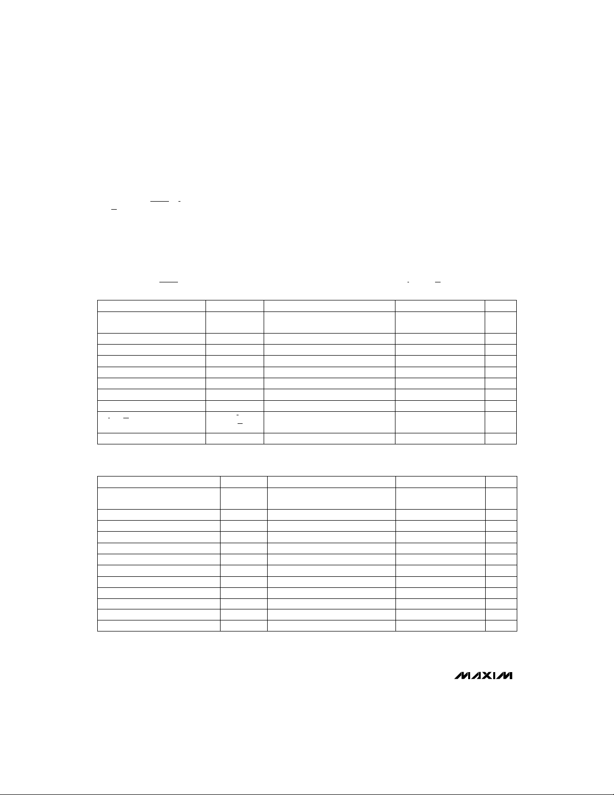
_______________Detailed Description
The following sections describe each of the functional
blocks shown in the
the Typical Application Block Diagram (Figure 1).
The demodulator contains a single-ended-to-differential
converter, two Gilbert-cell multipliers, and two fixed
gain stages. Internally, IF is terminated with a 400Ω
resistor to GND. The IF input signal is AC coupled into
the input amplifier, which has 14dB of gain. This amplified IF signal is fed into the I and Q channel mixers for
demodulation. The multipliers mix the IF signal with the
quadrature LO signals, resulting in baseband I and Q
signals. The conversion gain of the multipliers is 15dB.
These signals are further amplified by 21dB by the
baseband amplifiers. The baseband amplifier chains
are DC coupled.
Functional Diagram
Demodulator
. Also refer to
DOWNCONVERTER
2
0˚
90˚
MAX2451
÷8
Figure 1. Typical Application Block Diagram
A/D
2
A/D
POST
PROCESSING
Local Oscillator
The local-oscillator section is formed by an emitter-coupled differential pair. Figure 2 shows the local-oscillator
equivalent circuit schematic. An external LC resonant
tank determines the oscillation frequency, and the Q of
this resonant tank affects the oscillator phase noise.
The oscillation frequency is twice the IF frequency, for
easy generation of quadrature signals.
The oscillator may be overdriven by an external source.
The source should be AC coupled into TANK/TANK, and
should provide 200mVp-p levels. A choke (typically
2.2µH) is required between TANK and TANK. Differential
input impedance at TANK/TANK is 10kΩ. For singleended drive, connect an AC bypass capacitor (1000pF)
from TANK to GND, and AC couple TANK to the source.
The oscillator can be overdriven at frequencies up to
1GHz (500MHz IF), but conversion gain and prescaler
output levels will be somewhat reduced.
4 _______________________________________________________________________________________

LO_V
3V, Ultra-Low-Power
Quadrature Demodulator
MAX2451
CC
R
L
5k
Q3 Q4
Q1
Figure 2. Local-Oscillator Equivalent Circuit
R
L
5k
TANKTANK
Q2
TO QUADRATURE
GENERATOR AND
PRESCALER
Quadrature Phase Generator
The quadrature phase generator uses two latches to
divide the local-oscillator frequency by two, and generates two precise quadrature signals. Internal limiting
amplifiers shape the signals to approximate square
waves to drive the Gilbert-cell mixers. The inphase signal (at half the local oscillator frequency) is further
divided by four for the prescaler output.
Prescaler
The prescaler output, PRE_OUT, is buffered and swings
typically 0.35Vp-p with a 10kΩ and 6pF load. It can be
AC coupled to the input of a frequency synthesizer.
Master Bias
During normal operation, ENABLE should be above
VCC- 0.4V. Pulling the ENABLE input low shuts off the
master bias and reduces the circuit current to typically
2µA. The master bias section includes a bandgap reference generator and a PTAT (Proportional To Absolute
Temperature) current generator.
__________Applications Information
Figure 3 shows the implementation of a resonant tank
circuit. The inductor, two capacitors, and a dual varactor form the oscillator’s resonant circuit. In Figure 3, the
oscillator frequency ranges from 130MHz to 160MHz.
To ensure reliable start-up, the inductor is directly connected across the local oscillator’s tank ports. The two
33pF capacitors affect the Q of the resonant circuit.
Other values may be chosen to meet individual appli-
C1 = 33pF 47k
TANK
1
/2 KV1410
L = 100nH
1
/2 KV1410
TANK
C2 = 33pF
Figure 3. Typical Resonant Tank Circuit
10k
47k
0.1µF
V
CTRL
cation requirements. The oscillation frequency can be
determined using the following formula:
f
o
=
2LC
π
EQ EQ
1
where
C
EQ
=
1C11
1
++
C22C
VAR
C
+
STRAY
and
L L L
where C
STRAY
=+
EQ STRAY
= parasitic capacitance and L
STRAY
parasitic inductance.
To alter the oscillation frequency range, change the
inductance, the capacitance, or both. For best phasenoise performance, keep the Q of the resonant tank as
high as possible:
C
EQ
EQ
L
EQ
where R
QR
=
≈ 10kΩ (Figure 2).
EQ
The oscillation frequency can be changed by altering
the control voltage, V
CTRL
.
=
_______________________________________________________________________________________ 5

3V, Ultra-Low-Power
Quadrature Demodulator
________________________________________________________Package Information
INCHES MILLIMETERS
DIM
MAX2451
e
D
A
0.101mm
A1
B
0.004in.
C
0°-8°
L
Narrow SO
HE
SMALL-OUTLINE
PACKAGE
(0.150 in.)
A1
DIM
D
D
D
A
B
C
E
e
H
L
PINS
MAX
MIN
0.069
0.053
0.010
0.004
0.019
0.014
0.010
0.007
0.157
0.150
0.228
0.016
8
14
16
0.244
0.050
INCHES MILLIMETERS
MIN
MAX
0.189
0.197
0.337
0.344
0.386
0.394
MIN
1.35
0.10
0.35
0.19
3.80
5.80
0.40
MIN
4.80
8.55
9.80
1.270.050
MAX
1.75
0.25
0.49
0.25
4.00
6.20
1.27
MAX
5.00
8.75
10.00
21-0041A
Maxim cannot assume responsibility for use of any circuitry other than circuitry entirely embodied in a Maxim product. No circuit patent licenses are
implied. Maxim reserves the right to change the circuitry and specifications without notice at any time.
6
___________________Maxim Integrated Products, 120 San Gabriel Drive, Sunnyvale, CA 94086 (408) 737-7600
© 1995 Maxim Integrated Products Printed USA is a registered trademark of Maxim Integrated Products.
 Loading...