

For free samples & the latest literature: http://www.maxim-ic.com, or phone 1-800-998-8800.
For small orders, phone 1-800-835-8769.
________________General Description
The MAX2430 is a versatile, silicon RF power amplifier
that operates directly from a 3V to 5.5V supply, making
it suitable for 3-cell NiCd or 1-cell lithium-ion battery
applications. It is designed for use in the 800MHz to
1000MHz frequency range and, at 915MHz, can produce +21dBm (125mW) of output power with greater
than 32dB of gain at VCC= 3.6V.
A unique shutdown function provides an off supply current of typically less than 1µA to save power during
“idle slots” in time-division multiple-access (TDMA)
transmissions. An external capacitor sets the RF output
power envelope ramp time. External power control is
also possible over a 15dB range. The amplifier’s input
is matched on-chip to 50Ω. The output is an open collector that is easily matched to a 50Ω load with few
external components.
The MAX2430 is ideal as a driver amplifier for portable
and mobile telephone systems, or as a complete power
amplifier for other low-cost applications, such as those
in the 915MHz spread-spectrum ISM band. It is fabricated with Maxim’s high-frequency bipolar transistor
process and is available in a thermally enhanced,
16-pin narrow SO and miniature 16-pin PwrQSOP packages with heat slug.
________________________Applications
Digital Cordless Phones
915MHz ISM-Band Applications
Two-Way Pagers
Wireless LANs
Cellular Phones
AM and FM Analog Transmitters
____________________________Features
♦ Operates Over the 800MHz to 1000MHz Frequency
Range
♦ Delivers 125mW at 915MHz from +3.6V Supply
(100mW typical from +3.0V supply)
♦ Operates Directly from 3-Cell NiCd or 1-Cell
Lithium-Ion Battery
♦ Over 32dB Power Gain
♦ RF Power Envelope Ramping is Programmable
with One External Capacitor
♦ Input Matched to 50Ω (VSWR < 2:1)
♦ 15dB Output Power Control Range
♦ 1µA Typical Shutdown Current
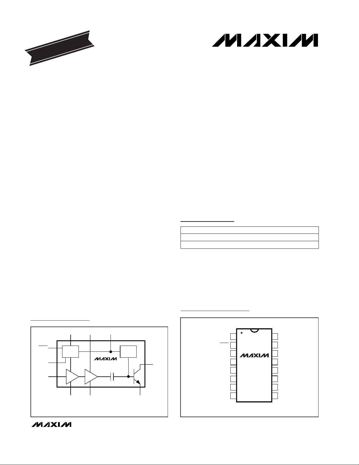
MAX2430
Low-Voltage, Silicon RF Power
Amplifier/Predriver
________________________________________________________________
Maxim Integrated Products
1
16
15
14
13
12
11
10
9
1
2
3
4
5
6
7
8
GND3
GND3
GND4
GND4
GND4
GND4
BIAS
RFOUT
GND3
SHDN
GND2
RFIN
GND2
GND1
VCC1
VCC2
TOP VIEW
MAX2430
Narrow SO/PwrQSOP
Pin Configuration
MAX2430
MASTER
BIAS
GAIN
GND2
NOTE: MAX2430IEE (PwrQSOP PACKAGE) UNDERSIDE METAL
SLUG MUST BE SOLDERED TO PCB GROUND PLANE.
GND3
VCC1 VCC2 BIAS
GND4
RFOUT
9
1087
11, 12, 13, 141, 15, 163, 5
SHDN
GND1
RFIN
2
6
4
DRIVER
OUTPUT
BIAS
Functional Diagram
19-1093; Rev 2; 1/98
PART TEMP. RANGE PIN-PACKAGE
EVALUATION KIT MANUAL
FOLLOWS DATA SHEET
Ordering Information
MAX2430IEE -20°C to +85°C 16 PwrQSOP
MAX2430ISE -20°C to +85°C 16 Narrow SO
MAX2430
Low-Voltage, Silicon RF Power
Amplifier/Predriver
2 _______________________________________________________________________________________
ABSOLUTE MAXIMUM RATINGS
DC ELECTRICAL CHARACTERISTICS
(VCC= VCC1 = VCC2 = RFOUT = 3V to 5.5V, GND1 = GND2 = GND3 = GND4 = 0V, SHDN = 2.2V, BIAS = open, RFIN = open,
T
A
= -20°C to +85°C, unless otherwise noted.)
AC ELECTRICAL CHARACTERISTICS
(MAX2430 EV kit, f = 915MHz, VCC= 3.6V, SHDN = VCC, RFOUT matched to 50Ω resistive load, output measurements taken after
matching network, T
A
= +25°C, unless otherwise noted.) (Note 1)
Stresses beyond those listed under “Absolute Maximum Ratings” may cause permanent damage to the device. These are stress ratings only, and functional
operation of the device at these or any other conditions beyond those indicated in the operational sections of the specifications is not implied. Exposure to
absolute maximum rating conditions for extended periods may affect device reliability.
VCC1, VCC2..........................................................................+6V
SHDN, BIAS...................................................-0.3V, (V
CC
+ 0.3V)
RFIN.............................................................................-0.3V, +2V
P
RFIN
..................................................................................-3dBm
Continuous Power Dissipation (T
A
= +70°C)
PwrQSOP (derate 20mW/°C above +70°C)......................1.6W
Narrow SO (derate 20mW/°C above +70°C) ....................1.6W
Operating Temperature Range ...........................-20°C to +85°C
Storage Temperature Range.............................-65°C to +160°C
Lead Temperature (soldering, 10sec).............................+300°C
SHDN = low
No RF input applied, VCC= 5.5V
BIAS pin open
SHDN = V
CC
CONDITIONS
µA110I
CC(OFF
)Shutdown Supply Current
mA52 70I
CC
V3 5.5V
CC
Supply Voltage Range
Supply Current
V2.2V
BIAS
BIAS Pin Voltage
V2.2 V
CC
V
SHDN(HI)
SHDN High Input
V0.4V
SHDN(LO)
SHDN Low Input
µA18I
SHDN
SHDN Bias Current
UNITSMIN TYP MAXSYMBOLPARAMETER
VCC= 3.0V
VCC= 3.6V
(Note 2)
P
RFIN
= -20dBm
f1 = 915MHz, f2 = 916MHz,
P
OUT
per tone = 14dBm
CONDITIONS
dBm
19 20.4
P
1dB
P
OUT
at 1dB Compression
20 21.4
MHz800 1000Frequency Range
32 34
dBG
P
Power Gain
dBc-30OIM3Output IM3
UNITSMIN TYP MAXSYMBOLPARAMETER
P
OUT
= P
1dB
P
OUT
= P
1dB
P
OUT
= P
1dB
P
OUT
= P
1dB
RFIN connected to 50Ω source
%24
η
Efficiency
dBc-40
dBc-262nd Harmonic
3rd Harmonic
mA160I
CCRF
Supply Current
2:1VSWR
IN
Maximum Input VSWR
VCC= 3V to 5.5V, P
RFIN
≤ -10dBm (Note 3) 8:1VSWR
OUT
Maximum Output Load
Mismatch
dB7NFNoise Figure
VCC= 3V to 5.5V, P
RFIN
≤ -12dBm (Note 4) 6:1VSWR
OUT
Maximum Output Load
Mismatch for Stability
31 33
MAX2430ISE
MAX2430IEE
MAX2430
Low-Voltage, Silicon RF Power
Amplifier/Predriver
_______________________________________________________________________________________
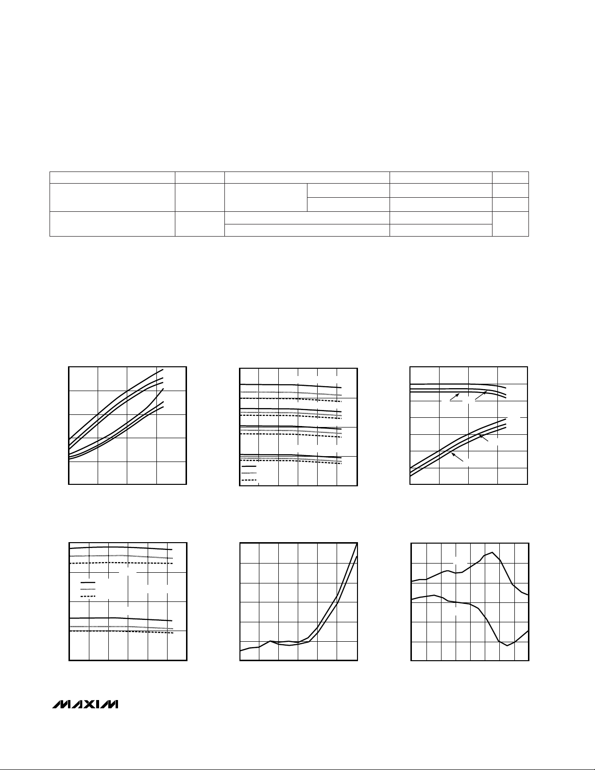
3
25
20
15
5
10
0
250
150
200
100
50
0
P
IN
(dBm)
-15-20 -5-10-25
OUTPUT POWER AND CURRENT
vs. INPUT POWER
P
OUT
(dBm)
I
CC
(mA)
P
OUT
3.6V
3.6V
5.5V
5.5V
3V
3V
I
CC
25
20
15
10
5
250
200
150
100
50
TEMPERATURE (°C)
-20 0 20 40 60 80 100
OUTPUT POWER AND CURRENT
vs. TEMPERATURE
P
OUT
(dBm)
I
CC
(mA)
-5.5V
3.6V
3V
P
OUT
@ PIN = -12dBm
P
OUT
@ PIN = -17dBm
ICC @ PIN = -17dBm
ICC @ PIN = -12dBm
30
35
40
25
20
15
10
5
MAX2430-03
PIN (dBm)
-15-20 -5-10-25
OUTPUT POWER AND GAIN
vs. INPUT POWER
P
OUT
(dBm) GAIN (dB)
P
OUT
3.6V
3.6V
5.5V
5.5V
3V
3V
GAIN
35
15
-20 40 60 80 100
OUTPUT POWER AND GAIN
vs. TEMPERATURE
(NORMAL OPERATING MODE)
20
30
MAX1691-4a
TEMPERATURE (°C)
25
20
0
5.5V
3.6V
3.0V
GAIN (dB)P
OUT
(dBm)
PIN = -12dBm
GAIN
P
OUT
4.0
3.5
3.0
2.0
1.5
2.5
1.0
MAX2430-05
FREQUENCY (MHz)
400 600 800 1000 1200 1400 1600
INPUT VSWR
vs. FREQUENCY
VSWR
3V
5V
150
100
50
-50
-100
0
-150
MAX2430-06
FREQUENCY (MHz)
800400 1200 1600 2000
RF INPUT IMPEDANCE
vs. FREQUENCY
INPUT IMPEDANCE (Ω)
REAL
IMAG
__________________________________________Typical Operating Characteristics
(MAX2430EVKIT-SO, f = 915MHz, VCC= 3.6V, SHDN = VCC, output matched to 50Ω resistive load, output measurements taken after
matching network, T
A
= +25°C, unless otherwise noted.)
Note 1: Minimum and maximum parameters are guaranteed by design.
Note 2: For optimum performance at a given frequency, output matching network must be designed for maximum output power.
See
Applications Information
section. Operation outside this frequency range is possible but has not been characterized.
Note 3: No damage to the device.
Note 4: All non-harmonically related outputs are more than 60dB below the desired signal for any electrical phase.
AC ELECTRICAL CHARACTERISTICS (continued)
(MAX2430 EV kit, f = 915MHz, VCC= 3.6V, SHDN = VCC, output matched to 50Ω resistive load, output measurements taken after
matching network, T
A
= +25°C, unless otherwise noted.) (Note 1)
CONDITIONS
BIAS pin capacitor C1 = 120pF
BIAS pin capacitor C1 = 2.2nF
dB50
µs
1
10
Turn-On/Off Times
UNITSMIN TYP MAXSYMBOLPARAMETER
SHDN = 0.4V,
P
IN
= -10dBm
dB47
RFIN to RFOUT Isolation
MAX2430ISE
MAX2430IEE

MAX2430
Low-Voltage, Silicon RF Power
Amplifier/Predriver
4 _______________________________________________________________________________________
_____________________________Typical Operating Characteristics (continued)
(MAX2430EVKIT-SO, f = 915MHz, VCC= 3.6V, SHDN = VCC, output matched to 50Ω resistive load, output measurements taken after
matching network, T
A
= +25°C, unless otherwise noted.)
1V/div
MAX2430-10
5µs/div
RF OUTPUT ENVELOPE CHARACTERISTICS
vs. SHUTDOWN CONTROL
VCC = 3.0V
BIAS CAPACITOR = 1nF
P
OUT
= 20.4dBm (110mW)
t
ON
≈ t
OFF
= 5µs
3V
0V
SHDN
3V
0V
25
20
15
10
5
0
-5
-10
-15
200
175
150
125
100
75
50
25
0
0.4 0.8 1.2 1.6 2.0 2.4
BIAS PIN VOLTAGE (V)
OUTPUT POWER AND SUPPLY CURRENT
vs. EXTERNAL CONTROL VOLTAGE
OUTPUT POWER (dBm)
I
CC
(mA)
TA = -20°C
TA = +25°C
TA = -20°C
TA = +85°C
PIN = -12dBm
V
CC
= 3.6V
TA = +85°C
I
CC
P
OUT
TA = +25°C
–
–
–
–
–
–
–
–
30
20
10
0
-10
-20
-30
-40
-50
-60
123456
MAX2430-07
HARMONIC NUMBER
OUTPUT POWER AND HARMONICS
OUTPUT SPECTRUM (dBm)
VCC = 3.0V
V
CC
= 3.6V
V
CC
= 4.5V
V
CC
= 5.5V
+20.4dBm
-4.93dBm
-16.7dBm
-47.6
dBm
-35.3dBm
-54.0
dBm
f1 = 915MHz
P
OUT
= +20.4dBm
-20
-25
-30
-35
-40
-45
-50
-55
-60
-65
-15 -10 -5 0 5 10 15 20
MAX2430-08
OUTPUT POWER PER TONE (dBm)
INTERMODULATION DISTORTION vs.
OUTPUT POWER AND TEMPERATURE
INTERMODULATION DISTORTION (dBc)
V
CC
= 3.6V
f1 = 915MHz
f2 = 916MHz
IM3
IM5
TA = -20°C
TA = -20°C
TA = +25°C
TA = +85°C
TA = +25°C
TA = +85°C
-20
-25
-30
-35
-40
-45
-50
-55
-60
-65
-70
-75
-10 -5 0 5 10 15 20
MAX2430-09
OUTPUT POWER PER TONE (dBm)
INTERMODULATION DISTORTION
vs. OUTPUT POWER AND V
CC
INTERMODULATION DISTORTION (dBc)
3.0V
3.6V
3.0V
3.6V
5.5V
5.5V
IM3
IM5

MAX2430
Low-Voltage, Silicon RF Power
Amplifier/Predriver
_______________________________________________________________________________________ 5
_____________________Pin Description
NAME FUNCTION
1, 15,
16
GND3
Driver Stage Ground. Connect directly to
ground plane.
2
SHDN
Shutdown Input (TTL/CMOS)
PIN
3, 5 GND2
Input Stage Ground. Connect directly to
ground plane.
4 RFIN
RF Input. Internally matched to 50Ω.
Requires series DC-blocking capacitor.
9 RFOUT Output Transistor. Open Collector.
8 VCC2
Driver Stage Output. Connect to supply
through inductor (see
Applications
Information
).
7 VCC1
Bias Circuitry Supply. Connect to supply.
Bypass with 1000pF capacitor.
6 GND1
Bias Circuitry Ground. Connect directly to
ground plane.
11–14 GND4
Output Stage Ground. Connect directly to
ground plane.
10 BIAS
Output Stage Bias Pin. Connect capacitor
to GND to control start-up power envelope. Drive directly for power control (see
Applications Information
).
Detailed Description
The MAX2430 consists of a large power output transistor driven by a capacitively coupled driver stage (see
Functional Diagram
). The driver and front-end gain
stages are DC-connected and biased on-chip from the
master bias cell. The master bias cell also controls the
output stage bias circuit. The input impedance at the
RFIN pin is internally matched to 50Ω, while the output
stage must be tuned and filtered externally for any narrow-band frequency range of interest between 800MHz
and 1000MHz.
The driver amplifier requires an external inductor at the
VCC2 pin to provide DC bias and proper matching to
the output stage. This inductor’s value depends on the
package type and frequency range of operation; typically it will vary between 5nH and 22nH.
The output transistor at the RFOUT pin requires an
external RF choke inductor connected to the supply for
DC bias, and a matching network to transform the
desired external load impedance to the optimal internal
load impedance of approximately 15Ω.
The MAX2430 includes a unique shutdown feature. The
TTL/CMOS-compatible SHDN input allows the device to
be shut down completely without the use of any external components. Also, the RF output power envelope
ramp time can be programmed with a single external
capacitor connected between the BIAS pin and
ground. Pulling the shutdown pin (SHDN) high powers
on the master bias circuit, which in turn charges the
external capacitor tied to the BIAS pin using a controlled current. The voltage at BIAS controls the output
power level, which ramps until the BIAS pin is internally
clamped to approximately 2.2V. The envelope rampdown time is controlled in a similar manner when the
SHDN pin is pulled low.
Variable output power control over a 15dB range is also
possible by forcing the voltage on the BIAS pin externally from 0.6V to 2.4V.
During the on state (SHDN = high), the power-supply
bias current is typically 52mA with no RF applied to the
input. During the off state (SHDN = low), the supply
current is typically reduced to less than 1µA.
Note:
MAX2430IEE (PwrQSOP package) underside metal slug
must be soldered to PCB ground plane.

MAX2430
Low-Voltage, Silicon RF Power
Amplifier/Predriver
6 _______________________________________________________________________________________
__________Applications Information
Output Matching
The optimum internal load impedance seen by RFOUT
is approximately 15Ω. This on-chip low drive impedance provides maximum power transfer and best efficiency under low (3V) supply conditions where the
voltage-swing headroom is limited. For example, driving an output power of 21.3dBm (135mW) into 50Ω
translates to a 7.35Vp-p swing at the output. An RF
amplifier would require at least a 4.5V supply to drive a
50Ω load directly. However, driving 21.3dBm into 15Ω
translates to 4.02Vp-p. The MAX2430 can achieve a
voltage swing of 4.02Vp-p or 2.01Vp from a 3V supply
voltage without saturating the output transistor.
Figure 1 shows the MAX2430 configured for 800MHz to
1000MHz operation. The output matching circuitry converts the desired 50Ω load impedance to the 15Ω optimal load seen by the output transistor’s collector. This
configuration uses a low-loss, controlled-Q inductor network. Starting from the RFOUT pin, this network consists
of a series L (which includes the 5nH package parasitic
inductance), series C, and shunt C. The design equations for this network are as follows:
R1 = Output resistance as seen by the
collector ~15Ω
RL= Desired load resistance
The controlled-Q inductor network requires that
R
L
> R1 and Q > . Choose Q and com-
pute matching components as given below:
where ω equals the center frequency in radians/second.
Recommended starting values for L1 and L2 are given
in Table 1.
Let A R x R1 R1
X Q x R1
X X A
X R x R1 / A
L1 = X / - 5nH of package
inductance
C =
1
X
C =
1
X
L
2
L
Co L
Csh L
L
O
Co
SH
Csh
=−
()
=
=−
=
ω
ω
ω
R / R1 1L −
()
MAX2430
OUTPUT
BIAS
GAIN
50Ω
˜
50Ω
GND2 GND3
VCC1
V
CC
V
CC
1nF
1nF 2.2nF
VCC2 BIAS
GND4
RFOUT
THREE-ELEMENT
MATCHING NETWORK
C
O
AND CSH TUNED FOR MAXIMUM POWER OUTPUT AT THE
DESIRED FREQUENCY BETWEEN 800MHz AND 1000MHz.
MAX2430IEE (PwrQSOP) UNDERSIDE METAL SLUG MUST
BE SOLDERED TO PCB GROUND PLANE.
L2 = 8nH FOR NARROW SO PACKAGE (MAX2430ISE)
L2 = 12nH FOR PwrQSOP PACKAGE (MAX2430IEE)
*
9
5nH
L
C
47nH
R
C
470Ω
L2*
RF OUTPUT
C
SH
C
O
L1
8nH
SHDN
ON
OFF
GND1
RFIN
C
IN
1nF
DRIVER
MASTER
BIAS
˜
15Ω
RF INPUT
R
L
Figure 1. Typical Application Circuit
L1(nH)
400 to 600* 22
800 to 1000 8
Table 1. Recommended L1 and L2 Starting
Values
*Not characterized
f = ω / 2π
(MHz)
600 to 800* 15
MAX2430ISE
L2(nH)
8
12
8
MAX2430IEE
L2(nH)
12
18
12

MAX2430
Low-Voltage, Silicon RF Power
Amplifier/Predriver
_______________________________________________________________________________________ 7
An overall loaded Q ≤ 5 can be achieved with readily
available surface-mount components. This network
absorbs the parasitic elements of the surface-mount
components in such a way that they do not negatively
impact the stopband characteristics; in fact, they can
improve the overall stopband attenuation with properly
chosen components. High-Q components (Q > 100)
that have self-resonance near the 3rd harmonic of the
intended output frequency should provide good passband characteristics with low loss, while offering good
attenuation of the undesired 2nd and 3rd harmonics
that are generated. Note that most applications will
require extra filtering components and good shielding
after the matching network to ensure absolute attenuation of out-of-band signals in order to meet out-of-band
spurious suppression requirements.
Output Mismatch Considerations
The MAX2430 will typically withstand an output load
mismatch of VSWR = 6:1 at any electrical phase without
exhibiting oscillatory behavior over the entire supply
voltage range of 3V to 5.5V. Resistor RCenhances stability under load mismatch conditions and does not
affect normal operation of the circuit.
BIAS Pin
The voltage at the BIAS pin controls the output power
transistor biasing. At BIAS = 0.6V, the output transistor
is biased to Class C, resulting in low gain and relatively
nonlinear power. Above 2V, the output stage is biased
to Class AB. Note that changing the bias voltage may
degrade the output transistor’s stability.
The shutdown pin (SHDN) controls the master bias circuit, which in turn provides a control current of approximately ±500µA to the external capacitor connected to
the BIAS pin. When SHDN transitions from low to high,
the BIAS pin capacitor charges up and clamps at
approximately 2.2V. When SHDN transitions from high
to low, the BIAS pin capacitor is discharged to nearly
ground. This results in a power-up/power-down ramping of the RF envelope, which can be approximated by
the following equation:
t
ramp
≅ C
BIAS
x 2.2V / 0.5mA = 4400Ω x C
BIAS
Therefore, a 2.2nF capacitor will give approximately
10µs ramp time.
The BIAS pin can also be used to control the final output
power and gain over a 15dB range, by forcing the BIAS
pin voltage externally between 0.6V and 2.4V. Note that
the BIAS pin driver must be able to source/sink 700µA.
Forcing the BIAS pin directly in this manner disrupts the
RF envelope timing function. To avoid this, place a
diode in series with the BIAS pin control circuit, as
shown in Figure 2.
Note that when using the BIAS pin for power control,
linearity is much degraded at the lower power levels.
Operating Frequency Range
The MAX2430 has been characterized for operation in
the 800MHz to 1000MHz range. Operation outside this
range is possible, but the following issues must be considered:
• Gain increases substantially at lower frequencies,
possibly causing stability problems.
• Useful gain and output power levels drop rapidly
above 1000MHz.
MAX2430
BIAS
10
0V TO 2.0V
POWER
CONTROL
2
C
BIAS
SHDN
MASTER
BIAS
2.2V
CLAMP
OUTPUT
BIAS
Figure 2. Power-Control Application Using BIAS Pin

MAX2430
Low-Voltage, Silicon RF Power
Amplifier/Predriver
8 _______________________________________________________________________________________
________________________________________________________Package Information
PSSOPPS.EPS

MAX2430
Low-Voltage, Silicon RF Power
Amplifier/Predriver
_______________________________________________________________________________________ 9
___________________________________________Package Information (continued)
SOICN.EPS

MAX2430
Low-Voltage, Silicon RF Power
Amplifier/Predriver
10 ______________________________________________________________________________________
NOTES
 Loading...