

________________General Description
The MAX2424/MAX2426 highly integrated front-end ICs
provide the lowest cost solution for cordless and ISMband radios operating in the 900MHz band. Both devices
incorporate a receive image-reject mixer (to reduce filter
cost) as well as a versatile transmit mixer. The devices
operate from a +2.7V to +4.8V single power supply,
allowing direct connection to a 3-cell battery stack.
The receive path incorporates an adjustable-gain LNA
and an image-reject downconverter with 35dB image
suppression. These features yield excellent combined
downconverter noise figure (4dB) and high linearity with
an input third-order intercept point (IIP3) of up to +2dBm.
The transmitter consists of a double-balanced mixer and
a power amplifier (PA) predriver that produces up to
0dBm (in some applications serving as the final power
stage). It can be used in a variety of configurations,
including BPSK modulation, direct VCO modulation, and
transmitter upconversion. For devices featuring transmit as well as receive image rejection, refer to the
MAX2420/MAX2421/MAX2422/MAX2460/MAX2463
data sheet.
The MAX2424/MAX2426 have an on-chip local oscillator
(LO), requiring only an external varactor-tuned LC tank
for operation. The integrated divide-by-64/65 dual-modulus prescaler can also be set to a direct mode, in which
it acts as an LO buffer amplifier. Four separate powerdown inputs can be used for system power management, including a 0.5µA shutdown mode.
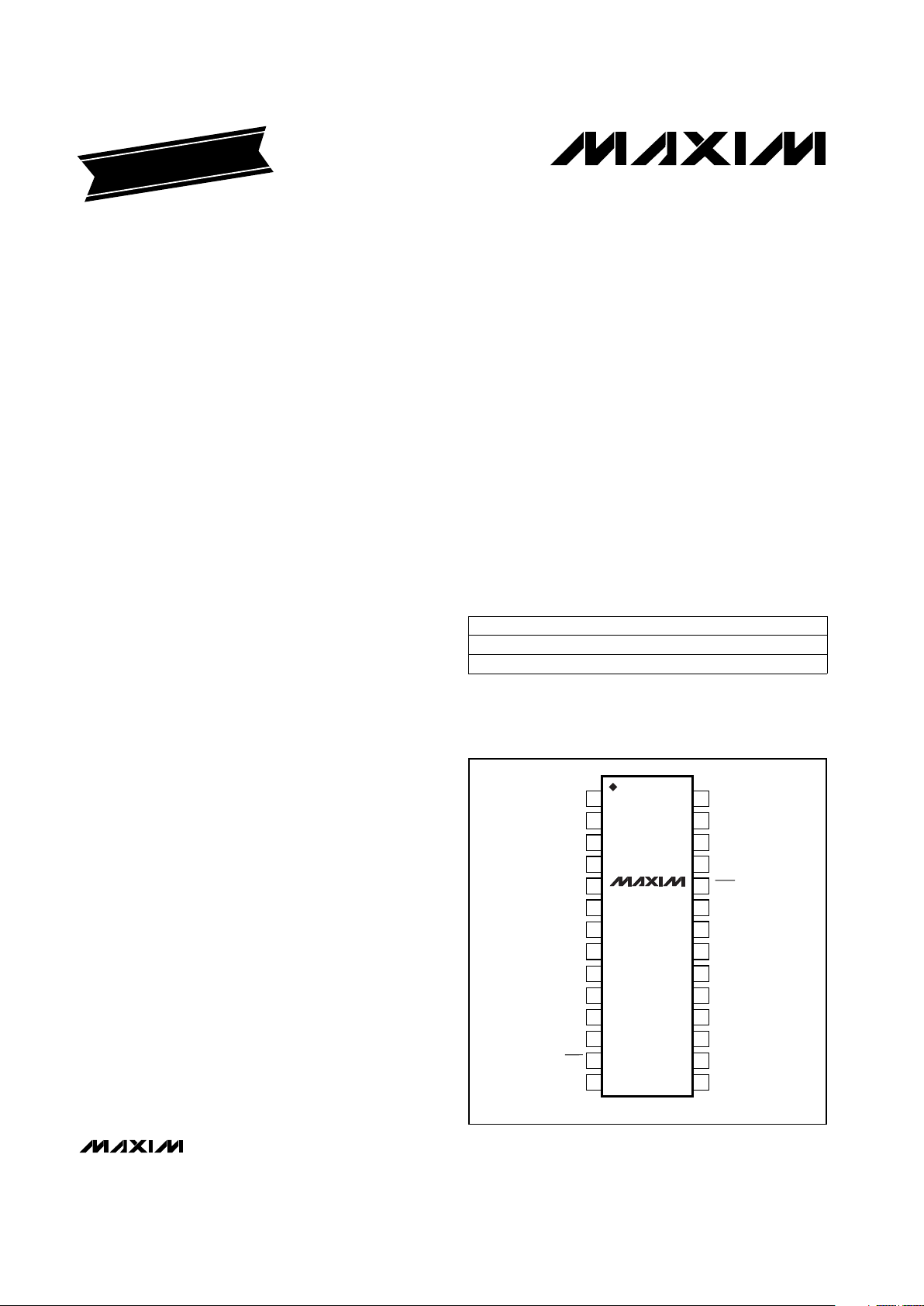
The MAX2424/MAX2426 come in a 28-pin SSOP package.
________________________Applications
Cordless Phones
Wireless Telemetry
Wireless Networks
Spread-Spectrum Communications
Two-Way Paging
____________________________Features
♦ Receive Mixer with 35dB Image Rejection
♦ Adjustable-Gain LNA
♦ Up to +2dBm Combined Receiver Input IP3
♦ 4dB Combined Receiver Noise Figure
♦ Optimized for Common Receiver IF Frequencies:
10.7MHz (MAX2424)
70MHz (MAX2426)
♦ PA Predriver Provides up to 0dBm
♦ Low Current Consumption: 23mA Receive
20mA Transmit
9.5mA Oscillator
♦ 0.5µA Shutdown Mode
♦ Operates from Single +2.7V to +4.8V Supply
MAX2424/MAX2426
900MHz Image-Reject Receivers
with Transmit Mixer
________________________________________________________________
Maxim Integrated Products
1
28
27
26
25
24
23
22
21
20
19
18
17
16
15
1
2
3
4
5
6
7
8
9
10
11
12
13
14
GND
GND
GND
TANK
TXON
PREOUT
PREGND
MOD
DIV1
VCOON
RXON
CAP2
TXIN
TXIN
LNAGAIN
TXOUT
GND
GND
RXIN
GND
RXOUT
CAP1
SSOP
TOP VIEW
MAX2424
MAX2426
TANK
V
CC
V
CC
V
CC
V
CC
V
CC
___________________Pin Configuration
19-1350 Rev 2; 2/99
PART
MAX2424EAI
-40°C to +85°C
TEMP. RANGE PIN-PACKAGE
28 SSOP
_______________Ordering Information
Functional Diagram appears at end of data sheet.
EVALUATION KIT MANUAL
FOLLOWS DATA SHEET
MAX2426EAI
-40°C to +85°C 28 SSOP
For free samples & the latest literature: http://www.maxim-ic.com, or phone 1-800-998-8800.
For small orders, phone 1-800-835-8769.
MAX2424/MAX2426
900MHz Image-Reject Receiver
with Transmit Mixer
2 _______________________________________________________________________________________
ABSOLUTE MAXIMUM RATINGS
DC ELECTRICAL CHARACTERISTICS
(VCC= +2.7V to +4.8V, no RF signals applied, LNAGAIN = Unconnected, V
TXIN
= V
TXIN
= 2.3V, V
VCOON
= 2.4V, V
RXON
= V
TXON
=
V
MOD
= V
DIV1
= 0.45V, PREGND = GND, TA= -40°C to +85°C. Typicals are at TA= +25°C, VCC= 3.3V, unless otherwise noted.)
Stresses beyond those listed under “Absolute Maximum Ratings” may cause permanent damage to the device. These are stress ratings only, and functional
operation of the device at these or any other conditions beyond those indicated in the operational sections of the specifications is not implied. Exposure to
absolute maximum rating conditions for extended periods may affect device reliability.
Note 1: Calculated by measuring the combined oscillator and prescaler supply current and subtracting the oscillator supply current.
Note 2: Calculated by measuring the combined oscillator and LO buffer supply current and subtracting the oscillator supply current.
Note 3: Calculated by measuring the combined receive and oscillator supply current and subtracting the oscillator supply current.
With LNAGAIN = GND, the supply current drops by 4.5mA.
Note 4: Calculated by measuring the combined transmit and oscillator supply current and subtracting the oscillator supply current.
V
CC
to GND...........................................................-0.3V to +5.5V
TXIN, TXIN Differential Voltage..............................................+2V
Voltage on TXOUT......................................-0.3V to (V
CC
+ 1.0V)
Voltage on LNAGAIN, TXON, RXON, VCOON,
DIV1, MOD, TXIN, TXIN............................-0.3V to (V
CC
+ 0.3V)
RXIN Input Power..............................................................10dBm
TANK, TANK Input Power...................................................2dBm
Continuous Power Dissipation (T
A
= +70°C)
SSOP (derate 9.50mW/°C above +70°C) ......................762mW
Operating Temperature Range ...........................-40°C to +85°C
Junction Temperature......................................................+150°C
Storage Temperature Range .............................-65°C to +165°C
Lead Temperature (soldering, 10sec) .............................+300°C
PARAMETER
MIN TYP MAX UNITS
Receive Supply Current (Note 3) 23 36 mA
Prescaler Supply Current
(buffer mode) (Note 2)
5.4 8.5 mA
Oscillator Supply Current
Supply-Voltage Range 2.7 4.8 V
9.5 14 mA
Prescaler Supply Current
(÷ 64/65 mode) (Note 1)
4.2 6 mA
CONDITIONS
V
RXON
= 2.4V, PREGND = unconnected
V
DIV1
= 2.4V
PREGND = unconnected
Digital Input Voltage Low 0.45 V
Shutdown Supply Current
0.5
RXON, TXON, DIV1, VCOON, MOD
VCOON = RXON = TXON
= MOD = DIV1 = GND
Digital Input Current ±1 ±10 µAVoltage on any one digital input = VCCor GND
Digital Input Voltage High V2.4RXON, TXON, DIV1, VCOON, MOD
10
µA
TA= +25°C
TA= -40°C to +85°C
Transmitter Supply Current (Note 4) 20 32 mA
V
RXON
= 0.45V, V
TXON
= 2.4V,
PREGND = unconnected
AC ELECTRICAL CHARACTERISTICS
(MAX2424/MAX2426 EV kit, VCC= +3.3V, f
RXIN
= 915MHz, P
RXIN
= -35dBm, V
TXIN
= V
TXIN
= 2.3V (DC bias), V
TXIN
= 250mVp-p,
f
TXIN
= 1MHz, V
LNAGAIN
= 2V, V
VCOON
= 2.4V, RXON = TXON = MOD = DIV1 = PREGND = GND, TA= +25°C, unless otherwise noted.)
MAX2424/MAX2426
900MHz Image-Reject Receiver
with Transmit Mixer
_______________________________________________________________________________________ 3
(Note 11)
MAX2424 (Notes 5, 6)
TA= T
MIN
to T
MAX
(Note 5)
TA= +25°C
(Notes 5, 6)
(Notes 5, 10)
(Note 9)
Receiver on or off
LNAGAIN = GND (Note 7)
V
LNAGAIN
= 1V (Note 7)
V
LNAGAIN
= 1V (Notes 5, 8)
LNAGAIN = V
CC
(Notes 5, 8)
V
LNAGAIN
= VCC,
TA= -40°C to +85°C (Notes 5, 7)
MAX2426 (Notes 5, 6)
V
LNAGAIN
= VCC,
TA= +25°C (Note 7)
V
LNAGAIN
= 1V (Notes 5, 7)
LNAGAIN = V
CC
(Notes 5, 7)
CONDITIONS
dBc30Carrier Suppression
dBm3.5Output Third-Order Intercept (OIP3)
dBm-0.5Output 1dB Compression
-10 -4.5
dBm
-9.5 -7 -5
Output Power
MHz125Baseband 3dB Bandwidth
MHz800 1000Output Frequency Range
ns500Receiver Turn-On Time
dBm-60LO to RXIN Leakage
-8
dB
-19 -17
Input Third-Order Intercept
(IIP3)
12
dB
45
Noise Figure
MHz
8.5 10.7 12.5
MHz800 1000Input Frequency Range
-16
12
18 24
19 25
55 70 85
IF Frequency Range
dB26 35Image Frequency Rejection
dB
20 22 24.5
Conversion Power Gain
19 21 23.5
UNITSMIN TYP MAXPARAMETER
MAX2424
MAX2426
MAX2424
MAX2426
V
LNAGAIN
= 1V
LNAGAIN = V
CC
-18
dBm
-26
Input 1dB Compression
(Note 12) ns220Transmitter Turn-On Time
dBm/Hz-140Output Noise Density
RECEIVER (V
RXON
= 2.4V, fLO= 925.7MHz (MAX2424), fLO= 985MHz (MAX2426))
TRANSMITTER (V
TXON
= 2.4V, fLO= 915MHz)
V
DIV1
= 2.4V, ZL= 50Ω,
MAX2424/MAX2426
900MHz Image-Reject Receiver
with Transmit Mixer
4 _______________________________________________________________________________________
AC ELECTRICAL CHARACTERISTICS (continued)
(MAX2424/MAX2426 EV kit, VCC= +3.3V, f
RXIN
= 915MHz, P
RXIN
= -35dBm, V
TXIN
= V
TXIN
= 2.3V (DC bias), V
TXIN
= 250mVp-p,
f
TXIN
= 1MHz, V
LNAGAIN
= 2V, V
VCOON
= 2.4V, RXON = TXON = MOD = DIV1 = PREGND = GND, TA= +25°C, unless otherwise noted.)
PARAMETER MIN TYP MAX UNITS
Oscillator Phase Noise
Oscillator Frequency Range 800 1100 MHz
82
dBc/Hz
(Note 5)
CONDITIONS
Note 5: Guaranteed by design and characterization.
Note 6: Image rejection typically falls to 30dBc at the frequency extremes.
Note 7: Refer to the
Typical Operating Characteristics
for a plot showing Receiver Gain vs. LNAGAIN Voltage, Input IP3 vs.
LNAGAIN Voltage, and Noise Figure vs. LNAGAIN Voltage.
Note 8: Two tones at P
RXIN
= -45dBm each, f1 = 915.0MHz and f2 = 915.2MHz.
Note 9: Time delay from V
RXON
= 0.45V to V
RXON
= 2.4V transition to the time the output envelope reaches 90% of its final value.
Note 10: Output power typically falls to -10dBm at the frequency extremes.
Note 11: Two tones at V
TXIN
= 125mVp-p, f1 = 1.0MHz, and f2 = 1.2MHz.
Note 12: Time delay from V
TXON
= 0.45V to V
TXON
= 2.4V transition to the time the output envelope reaches 90% of its final value.
Note 13: Using tank components L3 = 5.0nH (Coilcraft A02T), C2 = C3 = C26 = 3.3pF, R6 = R7 = 10Ω.
Note 14: This approximates a typical application in which TXOUT is followed by an external PA and a T/R switch with finite isolation.
Note 15: Relative to the rising edge of PREOUT.
Prescaler Output Level
500 mVp-p
-11 -8
Required Modulus Setup Time
(Notes 5, 15)
10 ns
ZL= 100kΩ
| |
10pF
÷ 64/65 mode
Required Modulus Hold Time
(Notes 5, 15)
0 ns
÷ 64/65 mode
Oscillator Buffer Output Level
(Notes 5, 13)
-12
dBm
V
DIV1
= 2.4V,
ZL= 50Ω
10kHz offset (Note 13)
72
Standby to TX or Standby to RX
35
Oscillator Pulling
8
kHz
110
RX to TX with P
RXIN
=-45dBm (RX mode)
to P
RXIN
= 0dBm (TX mode) (Note 14)
MAX2424
MAX2426
MAX2424
MAX2426
MAX2424
MAX2426
70
TA= +25°C
TA= -40°C to +85°C
OSCILLATOR AND PRESCALER
MAX2424/MAX2426
900MHz Image-Reject Receiver
with Transmit Mixer
_______________________________________________________________________________________
5
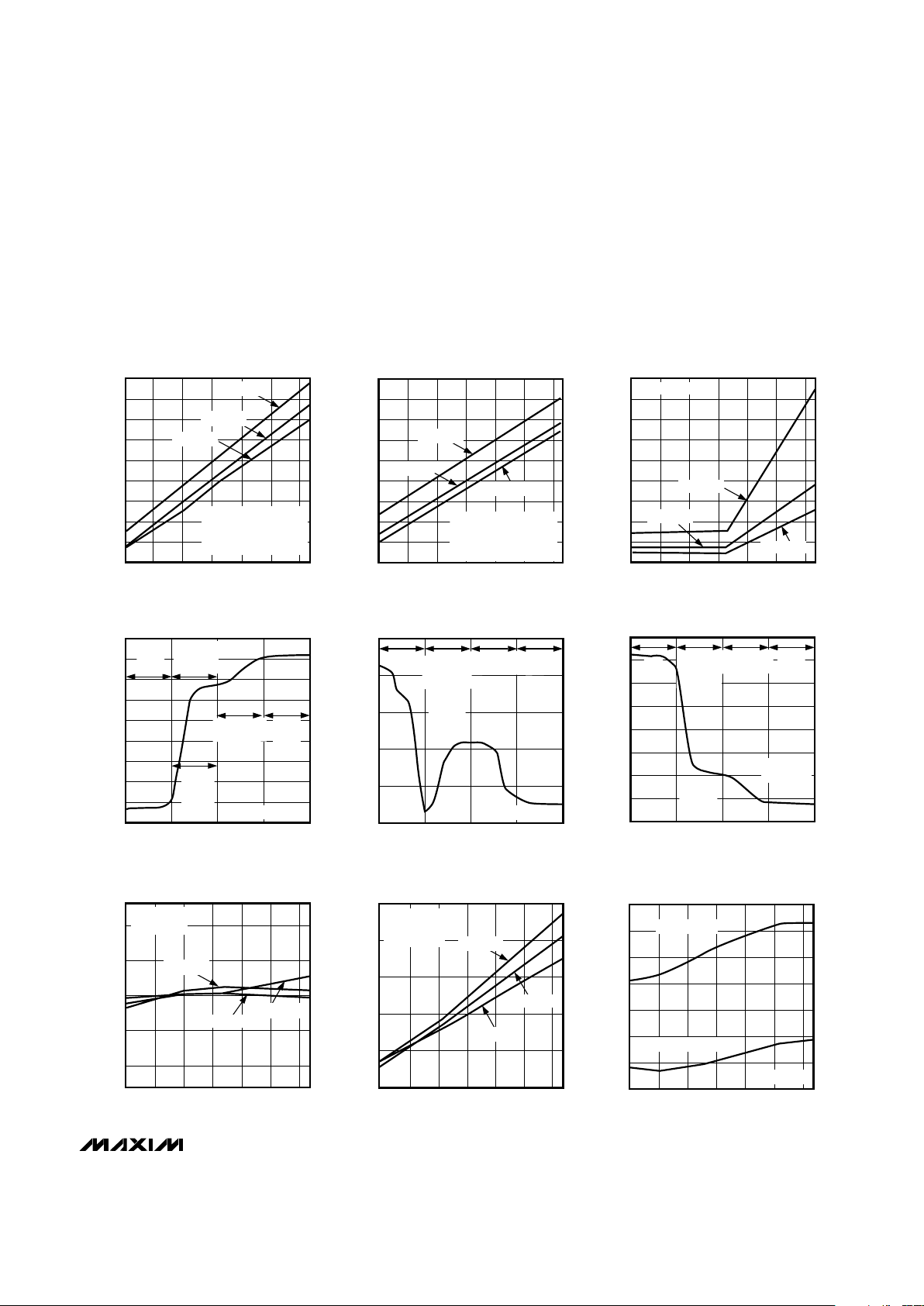
28
32
30
38
36
34
42
40
24
26
-40 0 20-20 40 60 80
RECEIVER SUPPLY CURRENT
vs. TEMPERATURE
MAX2424/6-01
TEMPERATURE (°C)
I
CC
(mA)
VCC = 2.7V
VCC = 3.3V
VCC = 4.8V
RXON = V
CC
PREGND = UNCONNECTED
INCLUDES OSCILLATOR
CURRENT
37
35
33
31
29
27
25
23
21
39
-40 0 20-20 40 60 80
TRANSMITTER SUPPLY CURRENT
vs. TEMPERATURE
MAX2424/6-02
TEMPERATURE (°C)
I
CC
(mA)
VCC = 2.7V
VCC = 3.3V
VCC = 4.8V
TXON = V
CC
PREGND = UNCONNECTED
INCLUDES OSCILLATOR
CURRENT
0
1.0
0.5
2.5
2.0
1.5
4.0
3.5
3.0
4.5
-40 0 20-20 40 60 80
SHUTDOWN SUPPLY CURRENT
vs. TEMPERATURE
MAX2424/6-03
TEMPERATURE (°C)
I
CC
(µA)
VCC = 2.7V
VCC = 3.3V
VCC = 4.8V
VCOON = GND
25
20
15
10
5
0
-5
-10
-15
-20
0 0.5 1.0 1.5 2.0
RECEIVER GAIN vs. LNAGAIN
MAX2424/6-04
LNAGAIN VOLTAGE (V)
RECEIVER GAIN (dB)
ADJUSTABLE
GAIN
MAX
GAIN
LNA
PARTIALLY
BIASED
LNA
OFF
AVOID
THIS
REGION
RXON = V
CC
18
22
20
26
24
-40 0 20-20 40 60 80
MAX2424
RECEIVER GAIN vs. TEMPERATURE
MAX2424/6-07
TEMPERATURE (°C)
RECEIVER GAIN (dB)
VCC = 2.7V
VCC = 3.3V
VCC = 4.8V
LNAGAIN = V
CC
RXON = V
CC
-20
-15
-10
-5
0
5
0 0.5 1.0 1.5 2.0
RECEIVER INPUT IP3 vs. LNAGAIN
MAX2424/6-05
LNAGAIN VOLTAGE (V)
IIP3 (dBm)
ADJUSTABLE
GAIN
AVOID
THIS
REGION
MAX
GAIN
LNA
PARTIALLY
BIASED
LNA
OFF
RXON = V
CC
0
5
15
10
25
20
30
40
35
0 0.5 1.0 1.5 2.0
RECEIVER NOISE FIGURE
vs. LNAGAIN
MAX2424/6-06
LNAGAIN VOLTAGE (V)
NOISE FIGURE (dB)
ADJUSTABLE
GAIN
AVOID
THIS
REGION
MAX
GAIN
LNA
PARTIALLY
BIASED
LNA
OFF
RXON = V
CC
DIV1 = V
CC
3.0
4.0
3.5
5.0
5.5
4.5
-40 0 20-20 40 60 80
RECEIVER NOISE FIGURE vs.
TEMPERATURE AND SUPPLY VOLTAGE
MAX2424/6-08
TEMPERATURE (°C)
NOISE FIGURE (dB)
VCC = 3.3V
LNAGAIN = V
CC
RXON = V
CC
DIV1 = V
CC
VCC = 4.8V
V
CC
= 2.7V
-20
-16
-18
-8
-10
-6
-12
-14
-40 0 20-20 40 60 80
RECEIVER INPUT IP3
vs. TEMPERATURE
MAX2424/6-09
TEMPERATURE (°C)
IIP3 (dBm)
V
LNAGAIN
= 1V
RXON = V
CC
V
LNAGAIN
= 2V
__________________________________________Typical Operating Characteristics
(MAX2424/MAX2426 EV kit, VCC= +3.3V; f
LO(
RX)
= 925.7MHz (MAX2424), 985MHz (MAX2426); f
RXIN
= 915MHz, P
RXIN
=
-35dBm, f
LO(TX)
= 915MHz, V
TXIN
= V
TXIN
= 2.3V (DC bias), V
TXIN
= 250mVp-p, f
TXIN
= 1MHz, V
LNAGAIN
= 2V, V
VCOON
= 2.4V,
RXON = TXON = MOD = DIV1 = PREGND = GND, TA= +25°C, unless otherwise noted.)

MAX2424/MAX2426
900MHz Image-Reject Receiver
with Transmit Mixer
6 _______________________________________________________________________________________
______________________________Typical Operating Characteristics (continued)
(MAX2424/MAX2426 EV kit, VCC= +3.3V; f
LO(
RX)
= 925.7MHz (MAX2424), 985MHz (MAX2426); f
RXIN
= 915MHz, P
RXIN
=
-35dBm, f
LO(TX)
= 915MHz, V
TXIN
= V
TXIN
= 2.3V (DC bias), V
TXIN
= 250mVp-p, f
TXIN
= 1MHz, V
LNAGAIN
= 2V, V
VCOON
= 2.4V,
RXON = TXON = MOD = DIV1 = PREGND = GND, TA= +25°C, unless otherwise noted.)
-20
10
-10
0
30
20
50
40
60
0 400 800 1200 1600 2000
RECEIVER IMAGE REJECTION
vs. RF FREQUENCY
MAX2424/6-11
RF FREQUENCY (MHz)
IMAGE REJECTION (dB)
RXON = V
CC
-9
-8
-4
-5
-3
-6
-7
-40 0 20-20 40 60 80
MAX2424
RECEIVER OUTPUT 1dB
COMPRESSION POINT vs. TEMPERATURE
MAX2424/6-10
TEMPERATURE (°C)
1dB COMPRESSION POINT (dBm)
VCC = 2.7V
VCC = 4.8V
RXON = V
CC
VCC = 3.3V
0
10
20
30
5
15
25
35
40
1 10 100 1000
RECEIVER IMAGE REJECTION
vs. IF FREQUENCY
MAX2424/6-12
IF FREQUENCY (MHz)
IMAGE REJECTION (dB)
RXON = V
CC
MAX2424 MAX2426
0
25
30
15
20
10
5
35
40
45
50
0
-60
-40
-20
-80
-100
800600 1000 1200 1400
RXIN INPUT IMPEDANCE
vs. FREQUENCY
MAX2424/6-13
FREQUENCY (MHz)
REAL IMPEDANCE (Ω)
IMAGINARY IMPEDANCE (Ω)
REAL
IMAGINARY
RXON = V
CC
-300
-200
-250
-50
-100
-150
0
50
100
150
800600 1000 1200 1400 1600 1800 2000
TXOUT OUTPUT IMPEDANCE
vs. FREQUENCY
MAX2424/6-16
FREQUENCY (MHz)
REAL OR IMAGINARY IMPEDANCE (Ω)
REAL
IMAGINARY
TXON = V
CC
5
-25
-15
-20
-5
-10
0
TRANSMITTER OUTPUT POWER
vs. INPUT VOLTAGE
MAX2424/6-14
INPUT VOLTAGE (mVp-p)
OUTPUT POWER (dBm)
10 100 1000
VCC = 2.7V
V
CC
= 4.8V
V
CC
= 3.3V
TXON = V
CC
-14
-2
-3
-4
-5
-6
-7
-8
-9
-10
-11
-12
-13
-40 0
20
-20
40 60 80
TRANSMITTER OUTPUT POWER
vs. TEMPERATURE
MAX2424/6-15
TEMPERATURE (°C)
OUTPUT POWER (dBm)
VCC = 2.7V
VCC = 4.8V
VCC = 3.3V
TXON = V
CC
-100
-80
-90
-60
-70
-40
-50
-30
-10
-20
0
910 912 913 914911 915 916 917 919918 920
TRANSMITTER OUTPUT SPECTRUM
MAX2424/6-17
FREQUENCY (MHz)
POWER (dBm)
DOUBLE-SIDE
BAND
FUNDAMENTAL
LO
TXON = V
CC
-7
-5
-6
-3
-4
0
-1
-2
1
-40 0-20 20 40 60 80
TRANSMITTER 1dB COMPRESSION POINT
vs. TEMPERATURE
MAX2424/6-18
TEMPERATURE (°C)
OUTPUT 1dB COMPRESSION (dBm)
VCC = 4.8V
VCC = 3.3V
VCC = 2.7V
TXON = V
CC

MAX2424/MAX2426
900MHz Image-Reject Receiver
with Transmit Mixer
_______________________________________________________________________________________
7
-36
3
0
-3
-6
-9
-12
-15
-18
-21
-24
-27
-30
-33
1 10 100 1000
TRANSMITTER BASEBAND
FREQUENCY RESPONSE
MAX2424/6-20
FREQUENCY (MHz)
TXOUT (dBc)
TXON = V
CC
-100
10
0
-10
-20
-30
-40
-50
-60
-70
-80
-90
10 100 1000
POWER vs. TXIN VOLTAGE
MAX2424/6-19
TXIN VOLTAGE (mVp-p)
POWER (dBm)
TXON = V
CC
NOTE: TXIN IS TOTAL
VOLTAGE FOR TWO TONES
(PEAK-TO-PEAK)
FUNDAMENTAL
IM3 LEVEL
______________________________Typical Operating Characteristics (continued)
(MAX2424/MAX2426 EV kit, VCC= +3.3V; f
LO(
RX)
= 925.7MHz (MAX2424), 985MHz (MAX2426); f
RXIN
= 915MHz, P
RXIN
=
-35dBm, f
LO(TX)
= 915MHz, V
TXIN
= V
TXIN
= 2.3V (DC bias), V
TXIN
= 250mVp-p, f
TXIN
= 1MHz, V
LNAGAIN
= 2V, V
VCOON
= 2.4V,
RXON = TXON = MOD = DIV1 = PREGND = GND, TA= +25°C, unless otherwise noted.)
______________________________________________________________Pin Description
Supply Voltage Input for the Receive Low-Noise Amplifier. Bypass with a 47pF low-inductance capacitor
to GND (pin 7 recommended).
6
Receiver RF Input, single ended. The input match shown in Figure 1 maintains an input VSWR of better
than 2:1 from 902MHz to 928MHz.
5
Ground Connection4
V
CC
RXIN
GND
Single-ended, 330Ω IF Output. AC couple to this pin. 3
Receive Bias Compensation Pin. Bypass with a 47pF low-inductance capacitor and 0.01µF to GND.
Do not make any other connections to this pin.
2
Supply-Voltage Input for Master Bias Cell. Bypass with a 47pF low-inductance capacitor and 0.1µF to
GND (pin 28 recommended).
1
FUNCTIONPIN
Low-Noise Amplifier Gain-Control Input. Drive this pin high for maximum gain. When LNAGAIN is pulled
low, the LNA is capacitively bypassed and the supply current is reduced by 4.5mA. This pin can also be
driven with an analog voltage to adjust the LNA gain in intermediate states. Refer to the Receiver Gain
vs. LNAGAIN Voltage graph in the
Typical Operating Characteristics,
as well as Table 1.
10
PA Predriver Output. See Figure 1 for an example matching network, which provides better than 2:1
VSWR from 902MHz to 928MHz.
9
LNAGAIN
TXOUT
Ground Connection for Receive Low-Noise Amplifier. Connect directly to ground plane using multiple
vias.
7 GND
RXOUT
CAP1
V
CC
NAME
Ground Connection for Signal-Path Blocks, except LNA8 GND
Supply Voltage Input for the Signal-Path Blocks, except LNA. Bypass with a 47pF low-inductance capacitor and 0.01µF to GND (pin 8 recommended).
11 V
CC

MAX2424/MAX2426
900MHz Image-Reject Receiver
with Transmit Mixer
8 _______________________________________________________________________________________
_________________________________________________Pin Description (continued)
FUNCTIONPIN NAME
Transmit Bias Compensation Input. Bypass with a 47pF low-inductance capacitor and 0.01µF to GND.
Do not make any other connections to this pin.
14
Transmit Mixer’s Inverting Baseband/IF Input. TXIN, TXIN form a high-impedance, differential input port.
See Figure 1.
13
CAP2
TXIN
Transmit Mixer’s Noninverting Baseband/IF Input. TXIN, TXIN form a high-impedance, differential input
port. See Figure 1.
12 TXIN
Prescaler/Oscillator Buffer Output. In divide-by-64/65 mode (DIV1 = low), the output level is 500mVp-p
into a high-impedance load. In divide-by-1 mode (DIV1 = high), this output delivers -8dBm into a 50Ω
load. AC couple to this pin.
21
Ground connection for the Prescaler. Connect PREGND to ground for normal operation. Leave unconnected to disable the prescaler and the output buffer. Connect MOD and DIV1 to ground and leave PREOUT unconnected when disabling the prescaler.
20
PREOUT
PREGND
Modulus Control for the Divide-by-64/65 Prescaler. Drive MOD high for divide-by-64 mode. Drive MOD
low for divide-by-65 mode.
19
Drive VCOON with a logic high to turn on the VCO, phase shifters, VCO buffers, and prescaler. To disable the prescaler, leave the PREGND pin unconnected.
17
Drive RXON and VCOON with a logic high to enable the LNA, receive mixer, and IF output buffer.
See
Power Management
section.
16
MOD
VCOON
RXON
Drive TXON and VCOON with a logic high to enable the transmit IF variable-gain amplifier, upconverter
mixer, and PA predriver. See
Power Management
section.
15 TXON
Drive DIV1 with a logic high to disable the divide-by-64/65 prescaler and connect the PREOUT pin
directly to an oscillator buffer amplifier, which outputs -8dBm into a 50Ω load. Drive DIV1 low for divideby-64/65 operation. Drive this pin low when in shutdown to minimize shutdown current.
18 DIV1
Supply-Voltage Input for Prescaler. Bypass with a 47pF low-inductance capacitor and 0.01µF to GND
(pin 20 recommended).
22 V
CC
Differential Oscillator Tank Port. See
Applications Information
for information on tank circuits or on using
an external oscillator.
24
TANK
Supply-Voltage Input for VCO and Phase Shifters. Bypass with a 47pF low-inductance capacitor to GND
(pin 26 recommended).
23 V
CC
Differential Oscillator Tank Port. See
Applications Information
for information on tank circuits or on using
an external oscillator.
25 TANK
Ground Connection for VCO and Phase Shifters26 GND
Ground (substrate)27 GND
Ground Connection for Master Bias Cell28 GND

MAX2424/MAX2426
900MHz Image-Reject Receiver
with Transmit Mixer
_______________________________________________________________________________________ 9
V
CC
V
CC
17
16
15
18
19
21
1000pF
VARACTORS:
ALPHA SMV1299-004
OR EQUIVALENT
WHEN USING DIFFERENTIAL
SOURCE, REMOVE RESISTORS
AND REPLACE CAPACITORS WITH
SHORTS. FOR SINGLE-ENDED
SOURCE, DRIVE ONLY MODULATOR
INPUT. CHOOSE R
A
AND RB VALUES
AS SHOWN IN
TRANSMITTER
SECTION.
RECEIVE IF OUTPUT (330Ω)
27
23
26
3
20
22
1
28
RECEIVE
RF INPUT
TRANSMIT
RF OUTPUT
5
9
7
6
0.01µF
47pF
V
CCVCC
0.1µF
V
CC
V
CC
V
CC
2
47pF
47pF
0.1µF
8.2nH
12nH
22nH
18nH
47pF
47pF
47pF
8
11
0.01µF
47pF
0.01µF
VCO TANK COMPONENTS
FOR 915MHz RF FREQUENCY
47pF
14
0.01µF
47pF
RXIN
TXOUT
GND
V
CC
V
CC
GND
GND
CAP2
GND
CAP1
V
CC
V
CC
TXON
RXON
VCOON
DIV1
MOD
PREOUT
TXON
RXON
VCOON
DIV1
MOD
TO PLL
GND
RXOUT
100nH
GND
PREGND
47pF
24
25
VCO
ADJUST
C3
1k
47k
47pF
1k
C2
C26
R6
R7
V
CC
V
CC
R
A
R
B
10k
10k
L3
TANK
MODULATOR INPUT
12
0.01µF*
TXIN
MODULATOR INPUT
13
0.01µF*
TXIN
LNAGAIN
LNAGAIN
4
47pF
10
MAX2424
MAX2426
TANK
*
MAX2424
MAX2426
DEVICE
10
20
R6, R7
(Ω)
2.0
4.0
C26
(pF)
6.8
3.3
L3
(nH)
3.3
8.0
C2, C3
(pF)
Figure 1. Typical Operating Circuit

MAX2424/MAX2426
900MHz Image-Reject Receiver
with Transmit Mixer
10 ______________________________________________________________________________________
_______________Detailed Description
The following sections describe each of the functional
blocks shown in the
Functional Diagram.
Receiver
The MAX2424/MAX2426’s receive path consists of a
900MHz low-noise amplifier, an image-reject mixer, and
an IF buffer amplifier.
The LNA’s gain and biasing are adjustable via the LNAGAIN pin. Proper operation of this pin provides optimum
performance over a wide range of signal levels. The LNA
has four modes determined by the DC voltage applied on
the LNAGAIN pin. See Table 1, as well as the relevant
Typical Operating Characteristics
plots.
At low LNAGAIN voltages, the LNA is shut off and the
input signal capacitively couples directly into mixer to
provide maximum linearity for large-signal operation
(receiver close to transmitter). As the LNAGAIN voltage
increases, the LNA turns on. Between 0.5V and 1V at
LNAGAIN, the LNA is partially biased and behaves like a
Class C amplifier. Avoid this operating mode for applications where linearity is a concern. As the LNAGAIN voltage reaches 1V, the LNA is fully biased into Class A
mode, and the gain is monotonically adjustable for LNAGAIN voltages above 1V. See the receiver gain, IP3, and
Noise Figure vs. LNAGAIN plots in the
Typical Operating
Characteristics
for more information.
The downconverter is implemented using an imagereject mixer consisting of an input buffer with two outputs, each of which is fed to a double-balanced mixer.
A quadrature LO drives the local-oscillator (LO) port of
each mixer. An on-chip oscillator and an external tank
circuit generates the LO. Its signal is buffered and split
into two phase shifters, which provide 90° of phase shift
across their outputs. This pair of LO signals is fed to the
mixers. The mixers’ outputs then pass through a second pair of phase shifters, which provide a 90° phase
shift across their outputs. The resulting mixer outputs are
then summed together. The final phase relationship is
such that the desired signal is reinforced and the image
signal is canceled. The downconverter mixer output
appears on the RXOUT pin, a single-ended 330Ω output.
Transmitter
The MAX2424/MAX2426 transmitter consists of a balanced mixer and a PA driver amplifier. The mixer inputs
are accessible via the TXIN and TXIN pins. An equivalent circuit for the TXIN and TXIN pins is shown in
Figure 2. Because TXIN and TXIN are linearly coupled
to the mixer stage, they can accept spectrally shaped
input signals. Typically, the mixer can be used to multiply the LO with a baseband signal, generating BPSK or
ASK modulation. Transmit upconversion can also be
implemented by applying a modulated IF signal to
these inputs. For applications requiring image rejection
on the transmitter, refer to the MAX2420/MAX2421/
MAX2422/MAX2460/MAX2463 data sheet.
Set the common-mode voltage at TXIN, TXIN to 2.3V by
selecting appropriate values for RAand RB(Figure 1). The
total series impedance of RAand RBshould be approximately 100kΩ.
Frequency modulation (FM) is realized by modulating
the VCO tuning voltage. Apply the appropriate differential and common-mode voltages to TXIN and TXIN to
control transmitter output power (Figure 3).
LNA partially biased. Avoid this
mode— the LNA operates in a
Class C manner
LNA capacitively bypassed,
minimum gain, maximum IP3
MODE
LNA at maximum gain
(remains monotonic)
LNA gain is monotonically
adjustable
1.5 < V
LNAGAIN
≤ V
CC
1.0 < V
LNAGAIN
≤ 1.5
0.5 < V
LNAGAIN
< 1.0
0 < V
LNAGAIN
≤ 0.5
LNAGAIN
VOLTAGE (V)
Table 1. LNA Modes
MAX2424
MAX2426
TXIN
2M
1.5µA
1.5µA
VMIXER INPUT
TXIN
Figure 2. TXIN, TXIN Equivalent Circuit

MAX2424/MAX2426
900MHz Image-Reject Receiver
with Transmit Mixer
______________________________________________________________________________________ 11
For example, if VCC= 3.3V and P
OUT
= -8dBm, choose
RT= 100kΩ for sufficient current through the divider, so
that bias currents for TXIN and TXIN have little effect
over temperature. Set V
TXIN
= 2.3V to satisfy common-
mode voltage range requirements at VCC= 3.3V.
Use the Transmit Output Power vs. Input Voltage graph
in the
Typical Operating Characteristics
to determine
the input voltage (in mVp-p) required to produce the
desired output. Divide this value by 2√2 and use it for
V
DIFF
. A -8dBm transmitter output requires 250mVp-p /
2√2 = 88.4mV.
V
TXIN
= 2.3V + 0.0884V = 2.3884V
RT= R1 + R2 + R3
Solve for resistors R1, R2, and R3 with the following
equations:
Since the transmit and receive sections typically require
different LO frequencies, it is not recommended to have
both transmit and receive active at the same time.
Phase Shifter
The MAX2424/MAX2426 uses passive networks to provide quadrature phase shifting for the receive IF and LO
signals. Because these networks are frequency selective, both the RF and IF frequency operating ranges are
limited. Image rejection degrades as the IF and RF
moves away from the designed optimum frequencies.
The MAX2424/MAX2426’s phase shifters are arranged
such that the LO frequency is higher than the RF carrier
frequency (high-side injection).
Local Oscillator (LO)
The on-chip LO is formed by an emitter-coupled differential pair. An external LC resonant tank sets the oscillation frequency. A varactor diode is typically used to
create a voltage-controlled oscillator (VCO). See the
Applications Information
section for an example VCO
tank circuit.
The LO may be overdriven in applications where an
external signal is available. The external LO signal
should be about 0dBm from 50Ω, and should be AC
coupled into either the TANK or TANK pin. Both TANK
and TANK require pull-up resistors to VCC. See the
Applications Information
section for details.
The local oscillator resists pulling caused by changes
in load impedance that occur as the part is switched
from standby mode, with just the oscillator running to
either transmit or receive mode. The amount of LO
pulling is affected if a signal is present at the RXIN port
in transmit mode. The most common cause of pulling is
imperfect isolation in an external transmit/
receive (T/R) switch. The
AC Electrical Characteristics
table contains specifications for this case as well.
Prescaler
The on-chip prescaler operates in two different modes:
as a dual-modulus divide-by-64/65, or as an oscillator
buffer amplifier. The DIV1 pin controls this function.
When DIV1 is low, the prescaler is in dual-modulus
divide-by-64/65 mode; when it is high, the prescaler is
disabled and the oscillator buffer amplifier is enabled.
The buffer typically outputs -8dBm into a 50Ω load. To
minimize shutdown supply current, pull the DIV1 pin
low when in shutdown mode.
In divide-by-64/65 drive mode, the division ratio is controlled by the MOD pin. Drive MOD high to operate the
prescaler in divide-by-64 mode. Drive MOD and DIV1
low to operate the prescaler in divide-by-65 mode.
R3
V x R
V
R2 V – V x
R
V
R1 R – R2 – R3
T
CC
TXIN
T
CC
T
=
=
()
=
TXIN
TXIN
RT = R1 + R2 + R
3
V
DIFF
= V
TXIN
- V
TXIN
R1 i
R2
R3
2M
V
CC
1.5µA
TXIN
1.5µA
TXIN
MAX2424
MAX2426
Figure 3. Biasing TXIN and TXIN for FM

To disable the prescaler entirely, leave PREGND and
PREOUT unconnected. Also connect the MOD and
DIV1 pins to GND. Disabling the prescaler does not
affect operation of the VCO stage.
Power Management
The MAX2424/MAX2426 supports four different powermanagement features to conserve battery life. The VCO
section has its own control pin (VCOON), which also
serves as a master bias pin. When VCOON is high, the
LO, quadrature LO phase shifters, and prescaler or LO
buffer are all enabled. Stabilize VCO by powering it up
prior to transmitting or receiving. For transmit-to-receive
switching, the receiver and transmitter sections have
their own enable control inputs, RXON and TXON. With
VCOON high, bringing RXON high enables the receive
path, which consists of the LNA, image-reject mixers,
and IF output buffer. When this pin is low, the receive
path is inactive. The TXON input enables the upconverter mixer and PA predriver. VCOON must be high for
the transmitter to operate. When TXON is low, the transmitter is off.
To disable all chip functions and reduce the supply current to typically 0.5µA, pull VCOON, DIV1, MOD, RXON,
and TXON low.
___________Applications Information
Oscillator Tank
The on-chip oscillator requires a parallel-resonant tank
circuit connected across TANK and TANK. Figure 4
shows an example of an oscillator tank circuit. Inductor
L4 provides DC bias to the tank ports. Inductor L3,
capacitor C26, and the series combination of capacitors C2, C3, and both halves of the varactor diode
capacitance set the resonant frequency as follows:
where CD1is the capacitance of one varactor diode.
Choose tank components according to your application
needs, such as phase-noise requirements, tuning
range, and VCO gain. High Q inductors such as aircore micro springs yield low phase noise. Use a lowtolerance inductor (L3) for predictable oscillation
frequency. Resistors R6 and R7 can be chosen from 0
to 20Ω to reduce the Q of parasitic resonance due to
series package inductance L
T
. Keep R6 and R7 as
small as possible to minimize phase noise, yet large
enough to ensure oscillator start-up in fundamental
mode. Oscillator start-up with be most critical with high
tuning bandwidth (low tank Q) and high temperature.
Capacitors C2 and C3 couple in the varactor. Light
coupling of the varactor is a way to reduce the effects
of high varactor tolerance and increase loaded Q. For a
wider tuning range, use larger values for C2 and C3 or
a varactor with a large capacitance ratio. Capacitor
C26 is used to trim the tank oscillator frequency. Larger
values for C26 will help negate the effect of stray PCB
capacitance and parasitic inductor capacitance (L3).
Choose a low-tolerance capacitor for C26.
C =
1
1C21
C32C
EFF
D1
++
+ C26
f =
1
2L3C
r
EFF
π
()
()
MAX2424/MAX2426
900MHz Image-Reject Receiver
with Transmit Mixer
12 ______________________________________________________________________________________
MAX2424
MAX2426
TANK
L3
6.8nH
L4
100nH
R5
1k
R4
1k
1/2 D1
1/2 D1
D1 = ALPHA SMV1299-004
SEE FIGURE 1 FOR R6, R7, C2, C3, C26, AND L3 COMPONENT VALUES.
C1
47pF
VCO_CTRL
R7
R6
C3
R8
47k
C2
C26
V
CC
TANK
Figure 4. Oscillator Tank Schematic Using the On-Chip VCO

For applications that require a wide tuning range and
low phase noise, a series-coupled resonant tank may
be required as shown in Figure 5. This tank will use the
package inductance in series with inductors L1, L2,
and capacitance of varactor D1 to set the net equivalent inductance which resonates in parallel with the
internal oscillator capacitance. Inductors L1 and L2
may be implemented as microstrip inductors, saving
component cost. Bias is provided to the tank port
through chokes L3 and L5. R1 and R3 should be chosen large enough to de-Q the parasitic resonance due
to L3 and L5 but small enough to minimize the voltage
drop across them due to bias current. Values for R1
and R3 should be kept between 0 and 50Ω. Proper
high frequency bypassing (C1) should be used for the
bias voltage to eliminate power supply noise from
entering the tank.
Oscillator Tank PC Board Layout
The parasitic PC board capacitance, as well as PCB
trace inductance and package inductance, affect oscillation frequency, so be careful in laying out the PC
board for the oscillator tank. Keep the tank layout as
symmetrical, tightly packed, and close to the device as
possible to minimize LO feedthrough. When using a PC
board with a ground plane, a cut-out in the ground
plane (and any other planes) below the oscillator tank
reduces parasitic capacitance.
Using an External Oscillator
If an external 50Ω LO signal source is available, it can
be used as an input to the TANK or TANK pin in place
of the on-chip oscillator (Figure 6). The oscillator signal
is AC coupled into the TANK pin and should have a
level of about 0dBm from a 50Ω source. For proper
biasing of the oscillator input stage, pull up the TANK
and TANK pins to the VCCsupply via 50Ω resistors.
If a differential LO source such as the MAX2620 is
available, AC-couple the inverting output into TANK.
MAX2424/MAX2426
900MHz Image-Reject Receiver
with Transmit Mixer
______________________________________________________________________________________ 13
MAX2424
TANK
50Ω
50Ω
50Ω
47pF
50Ω
EXT LO
EXTERNAL LO LEVEL IS 0dBm
FROM A 50Ω SOURCE.
V
CC
47pF
V
CC
TANK
Figure 6. Using an External Local Oscillator
MAX2424
MAX2426
TANK
L1
L
T
L
T
L2
L3
L4
L5
R1
R2
R3
C
i
1/2 D1
1/2 D1
C1C2
V
CC
V
TUNE
TANK
Figure 5. Series-Coupled Resonant Tank for Wide Tuning Range and Low Phase Noise

MAX2424/MAX2426
900MHz Image-Reject Receiver
with Transmit Mixer
14 ______________________________________________________________________________________
_________________________________________________________Functional Diagram
RXON
TXON
CAP2
TXOUT
CAP1
RXIN
LNAGAIN
90°
90°0°
0°
Σ
MAX2424
MAX2426
PHASE
SHIFTER
÷ 1/64/65
BIAS
RXOUT
DIV1
MOD
PREOUT
PREGND
TANK
TANK
VCOON
TXIN
0°
TXIN
________________________________________________________Package Information
SSOP.EPS
 Loading...