General Description
The MAX220–MAX249 family of line drivers/receivers is
intended for all EIA/TIA-232E and V.28/V.24 communications interfaces, particularly applications where ±12V is
not available.
These parts are especially useful in battery-powered systems, since their low-power shutdown mode reduces
power dissipation to less than 5µW. The MAX225,
MAX233, MAX235, and MAX245/MAX246/MAX247 use
no external components and are recommended for applications where printed circuit board space is critical.
________________________Applications
Portable Computers
Low-Power Modems
Interface Translation
Battery-Powered RS-232 Systems
Multidrop RS-232 Networks
____________________________Features
Superior to Bipolar
♦ Operate from Single +5V Power Supply
(+5V and +12V—MAX231/MAX239)
♦ Low-Power Receive Mode in Shutdown
(MAX223/MAX242)
♦ Meet All EIA/TIA-232E and V.28 Specifications
♦ Multiple Drivers and Receivers
♦ 3-State Driver and Receiver Outputs
♦ Open-Line Detection (MAX243)
Ordering Information
Ordering Information continued at end of data sheet.
*Contact factory for dice specifications.
MAX220–MAX249
+5V-Powered, Multichannel RS-232
Drivers/Receivers
________________________________________________________________ Maxim Integrated Products 1
Selection Table
19-4323; Rev 9; 4/00
PART
MAX220CPE
MAX220CSE
MAX220CWE 0°C to +70°C
0°C to +70°C
0°C to +70°C
TEMP. RANGE PIN-PACKAGE
16 Plastic DIP
16 Narrow SO
16 Wide SO
MAX220C/D 0°C to +70°C Dice*
MAX220EPE
MAX220ESE
MAX220EWE -40°C to +85°C
-40°C to +85°C
-40°C to +85°C 16 Plastic DIP
16 Narrow SO
16 Wide SO
MAX220EJE -40°C to +85°C 16 CERDIP
MAX220MJE -55°C to +125°C 16 CERDIP
Power No. of Nominal SHDN Rx
Part Supply RS-232 No. of Cap. Value & Three- Active in Data Rate
Number (V) Drivers/Rx Ext. Caps (µF) State SHDN (kbps) Features
MAX220 +5 2/2 4 4.7/10 No — 120 Ultra-low-power, industry-standard pinout
MAX222 +5 2/2 4 0.1 Yes — 200 Low-power shutdown
MAX223 (MAX213) +5 4/5 4 1.0 (0.1) Yes ✔ 120 MAX241 and receivers active in shutdown
MAX225 +5 5/5 0 — Yes ✔ 120 Available in SO
MAX230 (MAX200) +5 5/0 4 1.0 (0.1) Yes — 120 5 drivers with shutdown
MAX231 (MAX201) +5 and 2/2 2 1.0 (0.1) No — 120 Standard +5/+12V or battery supplies;
+7.5 to +13.2 same functions as MAX232
MAX232 (MAX202) +5 2/2 4 1.0 (0.1) No — 120 (64) Industry standard
MAX232A +5 2/2 4 0.1 No — 200 Higher slew rate, small caps
MAX233 (MAX203) +5 2/2 0 — No — 120 No external caps
MAX233A +5 2/2 0 — No — 200 No external caps, high slew rate
MAX234 (MAX204) +5 4/0 4 1.0 (0.1) No — 120 Replaces 1488
MAX235 (MAX205) +5 5/5 0 — Yes — 120 No external caps
MAX236 (MAX206) +5 4/3 4 1.0 (0.1) Yes — 120 Shutdown, three state
MAX237 (MAX207) +5 5/3 4 1.0 (0.1) No — 120 Complements IBM PC serial port
MAX238 (MAX208) +5 4/4 4 1.0 (0.1) No — 120 Replaces 1488 and 1489
MAX239 (MAX209) +5 and 3/5 2 1.0 (0.1) No — 120 Standard +5/+12V or battery supplies;
+7.5 to +13.2 single-package solution for IBM PC serial port
MAX240 +5 5/5 4 1.0 Yes — 120 DIP or flatpack package
MAX241 (MAX211) +5 4/5 4 1.0 (0.1) Yes — 120 Complete IBM PC serial port
MAX242 +5 2/2 4 0.1 Yes ✔ 200 Separate shutdown and enable
MAX243 +5 2/2 4 0.1 No — 200 Open-line detection simplifies cabling
MAX244 +5 8/10 4 1.0 No — 120 High slew rate
MAX245 +5 8/10 0 — Yes ✔ 120 High slew rate, int. caps, two shutdown modes
MAX246 +5 8/10 0 — Yes ✔ 120 High slew rate, int. caps, three shutdown modes
MAX247 +5 8/9 0 — Yes ✔ 120 High slew rate, int. caps, nine operating modes
MAX248 +5 8/8 4 1.0 Yes ✔ 120 High slew rate, selective half-chip enables
MAX249 +5 6/10 4 1.0 Yes ✔ 120 Available in quad flatpack package
For free samples & the latest literature: http://www.maxim-ic.com, or phone 1-800-998-8800.
For small orders, phone 1-800-835-8769.
MAX220–MAX249
+5V-Powered, Multichannel RS-232
Drivers/Receivers
2 _______________________________________________________________________________________
ABSOLUTE MAXIMUM RATINGS—MAX220/222/232A/233A/242/243
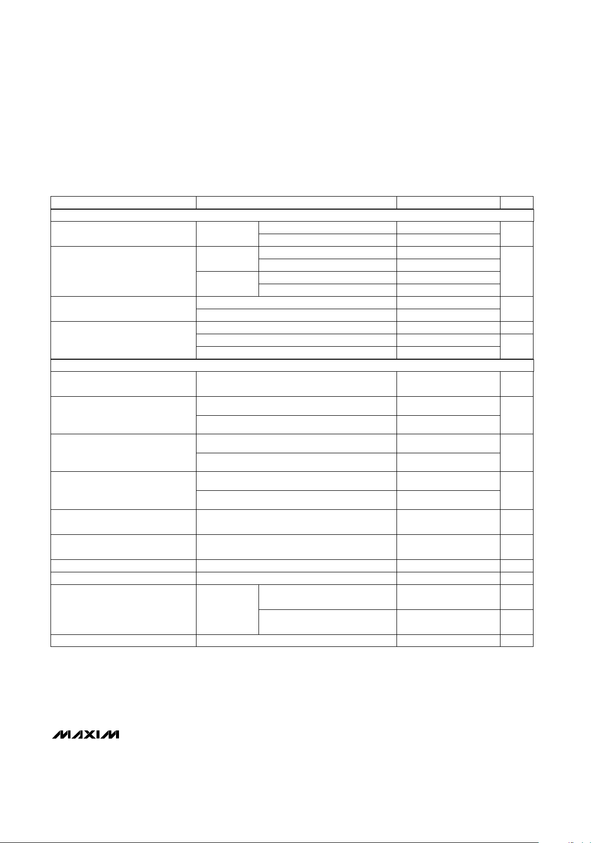
ELECTRICAL CHARACTERISTICS—MAX220/222/232A/233A/242/243
(VCC= +5V ±10%, C1–C4 = 0.1µF‚ MAX220, C1 = 0.047µF, C2–C4 = 0.33µF, TA= T
MIN
to T
MAX
‚ unless otherwise noted.)
Note 1: Input voltage measured with T
OUT
in high-impedance state, SHDN or VCC= 0V.
Note 2: For the MAX220, V+ and V- can have a maximum magnitude of 7V, but their absolute difference cannot exceed 13V.
Stresses beyond those listed under “Absolute Maximum Ratings” may cause permanent damage to the device. These are stress ratings only, and functional
operation of the device at these or any other conditions beyond those indicated in the operational sections of the specifications is not implied. Exposure to
absolute maximum rating conditions for extended periods may affect device reliability.
Supply Voltage (VCC) ...............................................-0.3V to +6V
Input Voltages
T
IN
..............................................................-0.3V to (VCC- 0.3V)
R
IN
(Except MAX220) ........................................................±30V
R
IN
(MAX220).....................................................................±25V
T
OUT
(Except MAX220) (Note 1) .......................................±15V
T
OUT
(MAX220)...............................................................±13.2V
Output Voltages
T
OUT
...................................................................................±15V
R
OUT
.........................................................-0.3V to (VCC+ 0.3V)
Driver/Receiver Output Short Circuited to GND.........Continuous
Continuous Power Dissipation (T
A
= +70°C)
16-Pin Plastic DIP (derate 10.53mW/°C above +70°C)....842mW
18-Pin Plastic DIP (derate 11.11mW/°C above +70°C)....889mW
20-Pin Plastic DIP (derate 8.00mW/°C above +70°C) ..440mW
16-Pin Narrow SO (derate 8.70mW/°C above +70°C) ...696mW
16-Pin Wide SO (derate 9.52mW/°C above +70°C)......762mW
18-Pin Wide SO (derate 9.52mW/°C above +70°C)......762mW
20-Pin Wide SO (derate 10.00mW/°C above +70°C)....800mW
20-Pin SSOP (derate 8.00mW/°C above +70°C) ..........640mW
16-Pin CERDIP (derate 10.00mW/°C above +70°C).....800mW
18-Pin CERDIP (derate 10.53mW/°C above +70°C).....842mW
Operating Temperature Ranges
MAX2_ _AC_ _, MAX2_ _C_ _.............................0°C to +70°C
MAX2_ _AE_ _, MAX2_ _E_ _ ..........................-40°C to +85°C
MAX2_ _AM_ _, MAX2_ _M_ _.......................-55°C to +125°C
Storage Temperature Range .............................-65°C to +160°C
Lead Temperature (soldering, 10sec) .............................+300°C
V
1.4 0.8Input Logic Threshold Low
UNITSMIN TYP MAXPARAMETER CONDITIONS
Input Logic Threshold High
All except MAX220 2 1.4
V
All except MAX220, normal operation 540
Logic Pull-Up/lnput Current
SHDN = 0V, MAX222/242, shutdown, MAX220
±0.01 ±1
µA
VCC= 5.5V, SHDN = 0V, V
OUT
= ±15V, MAX222/242
±0.01 ±10
Output Leakage Current
VCC= SHDN = 0V, V
OUT
= ±15V
±0.01 ±10
µA
All except MAX220, normal operation 200 116Data Rate kb/s
Transmitter Output Resistance VCC= V+ = V- = 0V, V
OUT
= ±2V 300 10M Ω
Output Short-Circuit Current V
OUT
= 0V ±7 ±22 mA
RS-232 Input Voltage Operating Range ±30 V
All except MAX243 R2
IN
0.8 1.3
RS-232 Input Threshold Low VCC= 5V
MAX243 R2IN(Note 2) -3
V
All except MAX243 R2
IN
1.8 2.4
RS-232 Input Threshold High VCC= 5V
MAX243 R2IN(Note 2) -0.5 -0.1
V
All except MAX243, V
CC
= 5V, no hysteresis in shdn. 0.2 0.5 1
RS-232 Input Hysteresis
MAX243 1
V
RS-232 Input Resistance 357kΩ
TTL/CMOS Output Voltage Low I
OUT
= 3.2mA 0.2 0.4 V
TTL/CMOS Output Voltage High I
OUT
= -1.0mA 3.5 VCC- 0.2 V
Sourcing V
OUT
= GND -2 -10
mATTL/CMOS Output Short-Circuit Current
Shrinking V
OUT
= V
CC
10 30
V±5 ±8Output Voltage Swing All transmitter outputs loaded with 3kΩ to GND
RS-232 TRANSMITTERS
RS-232 RECEIVERS
2.4MAX220: VCC= 5.0V
MAX220–MAX249
+5V-Powered, Multichannel RS-232
Drivers/Receivers
_______________________________________________________________________________________ 3
Note 3: MAX243 R2
OUT
is guaranteed to be low when R2INis ≥ 0V or is floating.
ELECTRICAL CHARACTERISTICS—MAX220/222/232A/233A/242/243 (continued)
(VCC= +5V ±10%, C1–C4 = 0.1µF‚ MAX220, C1 = 0.047µF, C2–C4 = 0.33µF, TA= T
MIN
to T
MAX
‚ unless otherwise noted.)
Operating Supply Voltage
SHDN Threshold High
4.5 5.5 V
MAX222/242
Transmitter-Output Enable Time
(SHDN goes high), Figure 4
2.0 1.4 V
MAX220 0.5 2
t
ET
No load
MAX222/232A/233A/242/243 410
MAX222/232A/233A/242/243 61230
MAX220 12
VCCSupply Current (SHDN = VCC),
Figures 5, 6, 11, 19
3kΩ load
both inputs
MAX222/232A/233A/242/243 15
mA
Transition Slew Rate
TA= +25°C 0.1 10
CL= 50pF to 2500pF,
R
L
= 3kΩ to 7kΩ,
V
CC
= 5V, TA= +25°C,
measured from +3V
to -3V or -3V to +3V
TA= 0°C to +70°C
CONDITIONS
250
MAX220 1.5 3 30
V/µs
TA= -40°C to +85°C 250
MAX222/242, 0.1µF caps
(includes charge-pump start-up)
Shutdown Supply Current MAX222/242
TA= -55°C to +125°C 35 100
µA
SHDN Input Leakage Current
MAX222/242 ±1 µA
SHDN Threshold Low
MAX222/242 1.4 0.8 V
250
MAX222/232A/233A/242/243 1.3 3.5
µs
t
PHLT
MAX220 410
Transmitter-Output Disable Time
(SHDN goes low), Figure 4
t
DT
MAX222/232A/233A/242/243 1.5 3.5
Transmitter Propagation Delay
TLL to RS-232 (normal operation),
Figure 1
t
PLHT
MAX220 510
µs
V2.0 1.4
MAX222/242, 0.1µF caps
µA±0.05 ±10
600
TTL/CMOS Output Leakage Current
EN Input Threshold High
MAX222/232A/233A/242/243 0.5 1
ns
t
PHLR
MAX220 0.6 3
t
PLHR
MAX222/232A/233A/242/243 0.6 1
Receiver Propagation Delay
RS-232 to TLL (normal operation),
Figure 2
t
PHLT
- t
PLHT
MAX220 0.8 3
µs
MAX222/232A/233A/242/243
t
PHLS
MAX242 0.5 10
Receiver Propagation Delay
RS-232 to TLL (shutdown), Figure 2
t
PLHS
MAX242 2.5 10
µs
Receiver-Output Enable Time, Figure 3 t
ER
MAX242
UNITSMIN TYP MAX
125 500
PARAMETER
MAX242
ns
SHDN = VCCor EN = V
CC
(SHDN = 0V for MAX222),
0V ≤ V
OUT
≤ V
CC
Receiver-Output Disable Time, Figure 3 t
DR
MAX242 160 500 ns
300
ns
Transmitter + to - Propagation
Delay Difference (normal operation)
MAX220 2000
t
PHLR
- t
PLHR
MAX222/232A/233A/242/243 100
ns
Receiver + to - Propagation
Delay Difference (normal operation)
MAX220 225
V1.4 0.8
EN Input Threshold Low
MAX242
MAX220–MAX249
+5V-Powered, Multichannel RS-232
Drivers/Receivers
4 _______________________________________________________________________________________
__________________________________________Typical Operating Characteristics
MAX220/MAX222/MAX232A/MAX233A/MAX242/MAX243
10
8
-10
0 5 15 25
OUTPUT VOLTAGE vs. LOAD CURRENT
-4
-6
-8
-2
6
4
2
MAX220-01
LOAD CURRENT (mA)
OUTPUT VOLTAGE (V)
10
0
20
0.1µF
EITHER V+ OR V- LOADED
V
CC
= ±5V
NO LOAD ON
TRANSMITTER OUTPUTS
(EXCEPT MAX220, MAX233A)
V- LOADED, NO LOAD ON V+
V+ LOADED, NO LOAD ON V-
1µF
1µF
0.1µF
11
10
4
010 40 60
AVAILABLE OUTPUT CURRENT
vs. DATA RATE
6
5
7
9
8
MAX220-02
DATA RATE (kbits/sec)
OUTPUT CURRENT (mA)
20 30 50
OUTPUT LOAD CURRENT
FLOWS FROM V+ TO V-
VCC = +5.25V
ALL CAPS
1µF
ALL CAPS
0.1µF
VCC = +4.75V
+10V
-10V
MAX222/MAX242
ON-TIME EXITING SHUTDOWN
+5V
+5V
0V
0V
MAX220-03
500µs/div
V+, V- VOLTAGE (V)
1µF CAPS
V+
V+
V-
V-
SHDN
0.1µF CAPS
1µF CAPS
0.1µF CAPS
MAX220–MAX249
+5V-Powered, Multichannel RS-232
Drivers/Receivers
_______________________________________________________________________________________ 5
VCC...........................................................................-0.3V to +6V
V+ ................................................................(V
CC
- 0.3V) to +14V
V- ............................................................................+0.3V to -14V
Input Voltages
T
IN
............................................................-0.3V to (VCC+ 0.3V)
R
IN
......................................................................................±30V
Output Voltages
T
OUT
...................................................(V+ + 0.3V) to (V- - 0.3V)
R
OUT
.........................................................-0.3V to (VCC+ 0.3V)
Short-Circuit Duration, T
OUT
......................................Continuous
Continuous Power Dissipation (T
A
= +70°C)
14-Pin Plastic DIP (derate 10.00mW/°C above +70°C)....800mW
16-Pin Plastic DIP (derate 10.53mW/°C above +70°C)....842mW
20-Pin Plastic DIP (derate 11.11mW/°C above +70°C)....889mW
24-Pin Narrow Plastic DIP
(derate 13.33mW/°C above +70°C) ..........1.07W
24-Pin Plastic DIP (derate 9.09mW/°C above +70°C)......500mW
16-Pin Wide SO (derate 9.52mW/°C above +70°C).........762mW
20-Pin Wide SO (derate 10 00mW/°C above +70°C).......800mW
24-Pin Wide SO (derate 11.76mW/°C above +70°C).......941mW
28-Pin Wide SO (derate 12.50mW/°C above +70°C) .............1W
44-Pin Plastic FP (derate 11.11mW/°C above +70°C) .....889mW
14-Pin CERDIP (derate 9.09mW/°C above +70°C) ..........727mW
16-Pin CERDIP (derate 10.00mW/°C above +70°C) ........800mW
20-Pin CERDIP (derate 11.11mW/°C above +70°C) ........889mW
24-Pin Narrow CERDIP
(derate 12.50mW/°C above +70°C) ..............1W
24-Pin Sidebraze (derate 20.0mW/°C above +70°C)..........1.6W
28-Pin SSOP (derate 9.52mW/°C above +70°C).............762mW
Operating Temperature Ranges
MAX2 _ _ C _ _......................................................0°C to +70°C
MAX2 _ _ E _ _ ...................................................-40°C to +85°C
MAX2 _ _ M _ _ ...............................................-55°C to +125°C
Storage Temperature Range .............................-65°C to +160°C
Lead Temperature (soldering, 10sec) .............................+300°C
ABSOLUTE MAXIMUM RATINGS—MAX223/MAX230–MAX241
ELECTRICAL CHARACTERISTICS—MAX223/MAX230–MAX241
(MAX223/230/232/234/236/237/238/240/241, VCC= +5V ±10; MAX233/MAX235, VCC= 5V ±5%‚ C1–C4 = 1.0µF; MAX231/MAX239,
V
CC
= 5V ±10%; V+ = 7.5V to 13.2V; TA= T
MIN
to T
MAX
; unless otherwise noted.)
Stresses beyond those listed under “Absolute Maximum Ratings” may cause permanent damage to the device. These are stress ratings only, and functional
operation of the device at these or any other conditions beyond those indicated in the operational sections of the specifications is not implied. Exposure to
absolute maximum rating conditions for extended periods may affect device reliability.
CONDITIONS
MIN TYP MAX
UNITS
Output Voltage Swing All transmitter outputs loaded with 3kΩ to ground ±5.0 ±7.3 V
VCCPower-Supply Current
No load,
TA= +25°C
510
mA
715
0.4 1
V+ Power-Supply Current
1.8 5
mA
515
Shutdown Supply Current TA= +25°C
15 50
VInput Logic Threshold High
T
IN
2.0
EN, SHDN (MAX223);
EN, SHDN (MAX230/235/236/240/241)
2.4
Logic Pull-Up Current T
IN
=0V 1.5 200
Receiver Input Voltage
Operating Range
-30 30 V
µA
µA
110
VInput Logic Threshold Low
TIN; EN, SHDN (MAX233); EN, SHDN (MAX230/235–241)
0.8
MAX231/239
MAX223/230/234–238/240/241
MAX232/233
PARAMETER
MAX239
MAX230/235/236/240/241
MAX231
MAX223
mA
MAX220–MAX249
+5V-Powered, Multichannel RS-232
Drivers/Receivers
6 _______________________________________________________________________________________
V
0.8 1.2
PARAMETER MIN TYP MAX UNITSCONDITIONS
Normal operation
SHDN = 5V (MAX223)
SHDN = 0V (MAX235/236/240/241)
1.7 2.4
RS-232 Input Threshold Low
TA= +25°C,
VCC= 5V
0.6 1.5
VRS-232 Input Threshold High
TA= +25°C,
VCC= 5V
Shutdown (MAX223)
SHDN = 0V,
EN = 5V (R4
IN
‚ R5IN)
1.5 2.4
ELECTRICAL CHARACTERISTICS—MAX223/MAX230–MAX241 (continued)
(MAX223/230/232/234/236/237/238/240/241, VCC= +5V ±10; MAX233/MAX235, VCC= 5V ±5%‚ C1–C4 = 1.0µF; MAX231/MAX239,
V
CC
= 5V ±10%; V+ = 7.5V to 13.2V; TA= T
MIN
to T
MAX
; unless otherwise noted.)
Shutdown (MAX223)
SHDN = 0V,
EN = 5V (R4
IN
, R5IN)
Normal operation
SHDN = 5V (MAX223)
SHDN = 0V (MAX235/236/240/241)
RS-232 Input Hysteresis VCC= 5V, no hysteresis in shutdown 0.2 0.5 1.0 V
RS-232 Input Resistance TA= +25°C, VCC= 5V 357kΩ
TTL/CMOS Output Voltage Low I
OUT
= 1.6mA (MAX231/232/233, I
OUT
= 3.2mA) 0.4 V
TTL/CMOS Output Voltage High I
OUT
= -1mA 3.5 VCC- 0.4 V
TTL/CMOS Output Leakage Current
0V ≤ R
OUT
≤ VCC; EN = 0V (MAX223);
EN = V
CC
(MAX235–241 )
0.05 ±10 µA
MAX223 600
nsReceiver Output Enable Time
Normal
operation
MAX235/236/239/240/241 400
MAX223 900
nsReceiver Output Disable Time
Normal
operation
MAX235/236/239/240/241 250
Normal operation 0.5 10
µs
SHDN = 0V
(MAX223)
440
Propagation Delay
RS-232 IN to
TTL/CMOS OUT,
CL= 150pF
640
3 5.1 30
V/µs
MAX231/MAX232/MAX233, TA= +25°C, VCC= 5V,
R
L
= 3kΩ to 7kΩ, CL= 50pF to 2500pF, measured from
+3V to -3V or -3V to +3V
430
Transmitter Output Resistance VCC= V+ = V- = 0V, V
OUT
= ±2V 300 Ω
Transmitter Output Short-Circuit
Current
±10 mA
t
PHLS
t
PLHS
Transition Region Slew Rate
MAX223/MAX230/MAX234–241, TA= +25°C, VCC= 5V,
RL= 3kΩ to 7kΩ‚ CL= 50pF to 2500pF, measured from
+3V to -3V or -3V to +3V
MAX220–MAX249
+5V-Powered, Multichannel RS-232
Drivers/Receivers
_______________________________________________________________________________________ 7
8.5
6.5
4.5 5.5
TRANSMITTER OUTPUT
VOLTAGE (V
OH
) vs. V
CC
7.0
8.0
MAX220-04
VCC (V)
V
OH
(V)
5.0
7.5
1 TRANSMITTER
LOADED
3 TRANSMITTERS
LOADED
4 TRANSMITTERS
LOADED
2 TRANSMITTERS
LOADED
TA = +25°C
C1–C4 = 1µF
TRANSMITTER
LOADS =
3kΩ || 2500pF
7.4
6.0
0 2500
TRANSMITTER OUTPUT VOLTAGE (VOH)
vs. LOAD CAPACITANCE AT
DIFFERENT DATA RATES
6.4
6.2
7.2
7.0
MAX220-05
LOAD CAPACITANCE (pF)
V
OH
(V)
15001000500 2000
6.8
6.6
160kbits/sec
80kbits/sec
20kbits/sec
TA = +25°C
V
CC
= +5V
3 TRANSMITTERS LOADED
R
L
= 3kΩ
C1–C4 = 1µF
12.0
4.0
0 2500
TRANSMITTER SLEW RATE
vs. LOAD CAPACITANCE
6.0
5.0
11.0
9.0
10.0
MAX220-06
LOAD CAPACITANCE (pF)
SLEW RATE (V/µs)
15001000500 2000
8.0
7.0
TA = +25°C
V
CC
= +5V
LOADED, R
L
= 3kΩ
C1–C4 = 1µF
1 TRANSMITTER LOADED
2 TRANSMITTERS
LOADED
3 TRANSMITTERS
LOADED
4 TRANSMITTERS
LOADED
-6.0
-9.0
4.5 5.5
TRANSMITTER OUTPUT
VOLTAGE (V
OL
) vs. V
CC
-8.0
-8.5
-6.5
-7.0
MAX220-07
VCC (V)
V
OL
(V)
5.0
-7.5
4 TRANSMITTERS
LOADED
TA = +25°C
C1–C4 = 1µF
TRANSMITTER
LOADS =
3kΩ || 2500pF
1 TRANSMITTER
LOADED
2 TRANSMITTERS
LOADED
3 TRANSMITTERS
LOADED
-6.0
-7.6
0 2500
TRANSMITTER OUTPUT VOLTAGE (VOL)
vs. LOAD CAPACITANCE AT
DIFFERENT DATA RATES
-7.0
-7.2
-7.4
-6.2
-6.4
MAX220-08
LOAD CAPACITANCE (pF)
V
OL
(V)
15001000500 2000
-6.6
-6.8
160kbits/sec
80kbits/sec
20Kkbits/sec
TA = +25°C
V
CC
= +5V
3 TRANSMITTERS LOADED
R
L
= 3kΩ
C1–C4 = 1µF
10
-10
0 5 10 15 20 25 30 35 40 45 50
TRANSMITTER OUTPUT VOLTAGE (V+, V-)
vs. LOAD CURRENT
-2
-6
-4
-8
8
6
MAX220-09
CURRENT (mA)
V+, V- (V)
4
2
0
V+ AND VEQUALLY
LOADED
V- LOADED,
NO LOAD
ON V+
TA = +25°C
V
CC
= +5V
C1–C4 = 1µF
ALL TRANSMITTERS UNLOADED
V+ LOADED,
NO LOAD
ON V-
__________________________________________Typical Operating Characteristics
MAX223/MAX230–MAX241
*SHUTDOWN POLARITY IS REVERSED
FOR NON MAX241 PARTS
V+, V- WHEN EXITING SHUTDOWN
(1µF CAPACITORS)
MAX220-13
SHDN*
V-
O
V+
500ms/div
Input Logic Threshold Low
MAX220–MAX249
+5V-Powered, Multichannel RS-232
Drivers/Receivers
8 _______________________________________________________________________________________
ABSOLUTE MAXIMUM RATINGS—MAX225/MAX244–MAX249
ELECTRICAL CHARACTERISTICS—MAX225/MAX244–MAX249
(MAX225, VCC= 5.0V ±5%; MAX244–MAX249, VCC= +5.0V ±10%, external capacitors C1–C4 = 1µF; TA= T
MIN
to T
MAX
; unless oth-
erwise noted.)
Note 4: Input voltage measured with transmitter output in a high-impedance state, shutdown, or V
CC
= 0V.
Stresses beyond those listed under “Absolute Maximum Ratings” may cause permanent damage to the device. These are stress ratings only, and functional
operation of the device at these or any other conditions beyond those indicated in the operational sections of the specifications is not implied. Exposure to
absolute maximum rating conditions for extended periods may affect device reliability.
Supply Voltage (VCC) ...............................................-0.3V to +6V
Input Voltages
T
IN
‚ ENA, ENB, ENR, ENT, ENRA,
ENRB, ENTA, ENTB..................................-0.3V to (V
CC
+ 0.3V)
R
IN
.....................................................................................±25V
T
OUT
(Note 3).....................................................................±15V
R
OUT
........................................................-0.3V to (VCC+ 0.3V)
Short Circuit (one output at a time)
T
OUT
to GND ............................................................Continuous
R
OUT
to GND............................................................Continuous
Continuous Power Dissipation (T
A
= +70°C)
28-Pin Wide SO (derate 12.50mW/°C above +70°C) .............1W
40-Pin Plastic DIP (derate 11.11mW/°C above +70°C) ...611mW
44-Pin PLCC (derate 13.33mW/°C above +70°C) ...........1.07W
Operating Temperature Ranges
MAX225C_ _, MAX24_C_ _ ..................................0°C to +70°C
MAX225E_ _, MAX24_E_ _ ...............................-40°C to +85°C
Storage Temperature Range .............................-65°C to +160°C
Lead Temperature (soldering,10sec) ..............................+300°C
VCC= 0V,
V
OUT
= ±15V
µATables 1a–1d
±0.01 ±25
Normal operation
Shutdown
Tables 1a–1d, normal operation
All transmitter outputs loaded with 3kΩ to GND
ENA, ENB, ENT, ENTA, ENTB =
V
CC,VOUT
= ±15V
VRS-232 Input Hysteresis
RS-232 Input Threshold Low V
V±5 ±7.5Output Voltage Swing
Output Leakage Current (shutdown)
±0.01 ±25
Ω300 10MVCC= V+ = V- = 0V, V
OUT
= ±2V (Note 4)Transmitter Output Resistance
µA
PARAMETER
±0.05 ±0.10
MIN TYP MAX UNITS
Normal operation, outputs disabled,
Tables 1a–1d, 0V ≤ V
OUT
≤ VCC, ENR_ = V
CC
TTL/CMOS Output Leakage Current
10 30Shrinking V
OUT
= V
CC
mA
-2 -10Sourcing V
OUT
= GND
V3.5 VCC- 0.2I
OUT
= -1.0mATTL/CMOS Output Voltage High
V0.2 0.4I
OUT
= 3.2mATTL/CMOS Output Voltage Low
kΩ357
0.2 0.5 1.0VCC= 5V
1.4 0.8 V
TTL/CMOS Output Short-Circuit Current
V1.8 2.4
0.8 1.3VCC= 5V
RS-232 Input Resistance
V±25RS-232 Input Voltage Operating Range
mA±7 ±30V
OUT
= 0VOutput Short-Circuit Current
kbits/sec120 64Data Rate
CONDITIONS
VCC= 5V
µA
±0.01 ±1
Logic Pull-Up/lnput Current
10 50
Tables 1a–1d
RS-232 Input Threshold High
V2 1.4Input Logic Threshold High
RS-232 TRANSMITTERS
RS-232 RECEIVERS
MAX220–MAX249
+5V-Powered, Multichannel RS-232
Drivers/Receivers
_______________________________________________________________________________________ 9
Operating Supply Voltage
4.75 5.25
V
Transmitter Enable Time
MAX225 10 20
t
ET
No load
MAX244–MAX249 11 30
51030
MAX225 40
VCCSupply Current
(normal operation)
3kΩ loads on
all outputs
MAX244–MAX249 57
mA
Transition Slew Rate
825
CL= 50pF to 2500pF, RL= 3kΩ to 7kΩ, VCC= 5V,
T
A
= +25°C, measured from +3V to -3V or -3V to +3V
TA= T
MIN
to T
MAX
CONDITIONS
50
V/µs
MAX246–MAX249
(excludes charge-pump start-up)
Shutdown Supply Current µA
5
t
PHLT
1.3 3.5
µs
t
PLHT
1.5 3.5
Transmitter Disable Time, Figure 4
Transmitter Propagation Delay
TLL to RS-232 (normal operation),
Figure 1
µs
t
DT
100 ns
Transmitter + to - Propagation
Delay Difference (normal operation)
t
PHLT
- t
PLHT
UNITSMIN TYP MAX
350
PARAMETER
ns
Receiver + to - Propagation
Delay Difference (normal operation)
t
PHLR
- t
PLHR
350 ns
4.5 5.5MAX244–MAX249
MAX225
Leakage current ±1
Threshold low 1.4 0.8
Control Input
Threshold high 2.4 1.4
V
µA
TA= +25°C
t
PHLR
0.6 1.5
t
PLHR
0.6 1.5
Receiver Propagation Delay
TLL to RS-232 (normal operation),
Figure 2
µs
t
PHLS
0.6 10
t
PLHS
3.0 10
Receiver Propagation Delay
TLL to RS-232 (low-power mode),
Figure 2
µs
Receiver-Output Enable Time, Figure 3 t
ER
100 500 ns
Receiver-Output Disable Time, Figure 3 t
DR
100 500 ns
MAX225/MAX245–MAX249
(includes charge-pump start-up)
10 ms
POWER SUPPLY AND CONTROL LOGIC
AC CHARACTERISTICS
Note 5: The 300Ω minimum specification complies with EIA/TIA-232E, but the actual resistance when in shutdown mode or VCC=
0V is 10MΩ as is implied by the leakage specification.
ELECTRICAL CHARACTERISTICS—MAX225/MAX244–MAX249 (continued)
(MAX225, VCC= 5.0V ±5%; MAX244–MAX249, VCC= +5.0V ±10%, external capacitors C1–C4 = 1µF; TA= T
MIN
to T
MAX
; unless oth-
erwise noted.)
MAX220–MAX249
+5V-Powered, Multichannel RS-232
Drivers/Receivers
10 ______________________________________________________________________________________
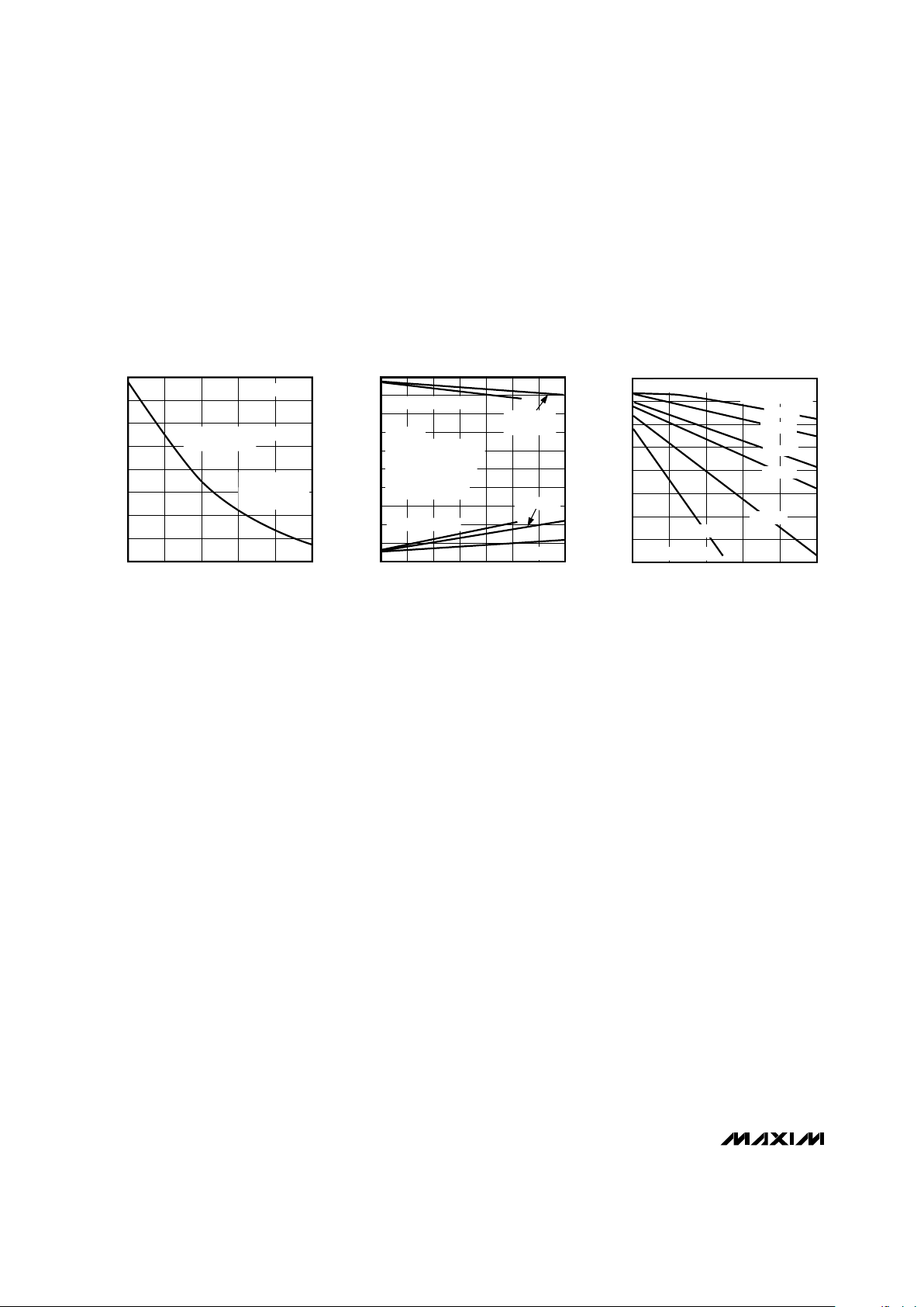
__________________________________________Typical Operating Characteristics
MAX225/MAX244–MAX249
18
2
012345
TRANSMITTER SLEW RATE
vs. LOAD CAPACITANCE
8
6
4
16
MAX220-10
LOAD CAPACITANCE (nF)
TRANSMITTER SLEW RATE (V/µs)
14
12
10
V
CC
= 5V
EXTERNAL POWER SUPPLY
1µF CAPACITORS
40kb/s DATA RATE
8 TRANSMITTERS
LOADED WITH 3kΩ
10
-10
0 5 10 15 20 25 30 35
OUTPUT VOLTAGE
vs. LOAD CURRENT FOR V+ AND V-
-2
-4
-6
-8
8
MAX220-11
LOAD CURRENT (mA)
OUTPUT VOLTAGE (V)
6
4
2
0
V+ AND V- LOADED
EITHER V+ OR
V- LOADED
V+ AND V- LOADED
VCC = 5V
EXTERNAL CHARGE PUMP
1µF CAPACITORS
8 TRANSMITTERS
DRIVING 5kΩ AND
2000pF AT 20kbits/sec
V- LOADED
V+ LOADED
9.0
5.0
01
2
345
TRANSMITTER OUTPUT VOLTAGE (V+, V-)
vs. LOAD CAPACITANCE AT
DIFFERENT DATA RATES
6.0
5.5
8.5
MAX220-12
LOAD CAPACITANCE (nF)
V+, V (V)
8.0
7.5
7.0
6.5
VCC = 5V WITH ALL TRANSMITTERS DRIVEN
LOADED WITH 5kΩ
10kb/sec
20kb/sec
40kb/sec
60kb/sec
100kb/sec
200kb/sec
ALL CAPACITIORS 1µF
MAX220–MAX249
+5V-Powered, Multichannel RS-232
Drivers/Receivers
______________________________________________________________________________________ 11
INPUT
OUTPUT
+3V
V+
0V
V-
0V
t
PLHT
t
PHLT
t
PHLR
t
PHLS
t
PLHR
t
PLHS
50%
V
CC
50%
+3V
50%
INPUT
OUTPUT
*EXCEPT FOR R2 ON THE MAX243
WHERE -3V IS USED.
0V*
50%
GND
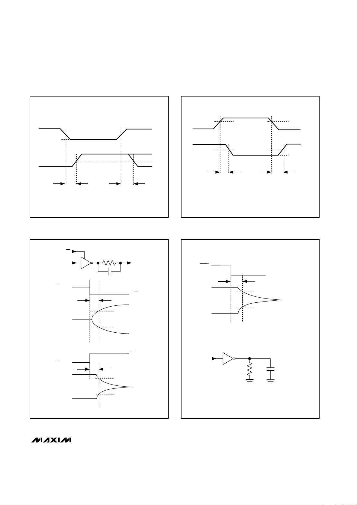
Figure 1. Transmitter Propagation-Delay Timing
Figure 2. Receiver Propagation-Delay Timing
EN
R
X
IN
a) TEST CIRCUIT
b) ENABLE TIMING
c) DISABLE TIMING
EN INPUT
RECEIVER
OUTPUTS
R
X
OUT
R
X
1k
0V
+3V
EN
EN
+0.8V
+3.5V
OUTPUT ENABLE TIME (t
ER
)
V
CC
- 2V
V
OL
+ 0.5V
V
OH
- 0.5V
OUTPUT DISABLE TIME (t
DR
)
V
CC
- 2V
+3V
0V
150pF
EN INPUT
V
OH
RECEIVER
OUTPUTS
V
OL
1 OR 0
T
X
3k
50pF
-5V
+5V
OUTPUT DISABLE TIME (t
DT
)
V+
SHDN
+3V
0V
V-
0V
a) TIMING DIAGRAM
b) TEST CIRCUIT
Figure 3. Receiver-Output Enable and Disable Timing
Figure 4. Transmitter-Output Disable Timing
 Loading...