

_______________General Description
The MAX2402 transmitter integrates a double-balanced
mixer, buffered local oscillator (LO) port, variable gain
stage, and power amplifier into a single IC. It is intended for use in the 800MHz to 1000MHz band, and is
compatible with both direct-sequence and frequencyhopping spread-spectrum designs in the 902MHz to
928MHz ISM band.
In a typical application, a digital baseband signal is
mixed with a local oscillator signal to yield a BPSKmodulated carrier at the antenna. Alternatively, the
baseband input may be grounded and an FSKmodulated LO signal applied directly to the LO port.
The LO port consists of a limiting amplifier that can
accept a single-ended or differential signal with input
power between -6dBm and +6dBm in the 800MHz to
1000MHz frequency range. The baseband modulation
input is linear over a 2V range, and limits with larger
signal levels within the supply range. The doublebalanced mixer has been optimized for high carrier
rejection. The variable gain stage offers typically 40dB
of adjustment range. The power amplifier provides
more than 20dBm output power and has a bias adjustment, which allows adjustment of efficiency and
harmonic distortion.
A shutdown function reduces the current draw to less
than 2µA in less than 10µs. The MAX2402 comes in a
20-pin SSOP package to minimize board area.
________________________Applications
Direct-Sequence Spread-Spectrum Transmitter
Frequency-Hopping Spread-Spectrum
Transmitter
FSK, GMSK, BPSK, and ASK Digital Transmitter
AM and FM Analog Transmitter
____________________________Features
♦ Low-Cost, Flexible Transmitter
♦ More than 100mW of Output Power into 50Ω
♦ Operates from 800MHz to 1000MHz
♦ Single +5V Supply
♦ 20-Pin SSOP Package
♦ Uses Less than 2µA in Power-Down
♦ More than 35dB of Power Adjustment Range
♦ LO Input Power Range from -6dBm to +6dBm
♦ 2V Linear Range on Modulation Input
MAX2402
800MHz to 1000MHz Transmitter
________________________________________________________________
Maxim Integrated Products
1
20
19
18
17
16
15
14
13
1
2
3
4
5
6
7
8
GND
V
CC
GND
GND
V
CC
GND
MOD
VGC
TOP VIEW
OUT
GND
OUT
GNDGND
LO-
LO+
GND
12
11
9
10
V
CC
LGND
BADJ
SHDN
SSOP
MAX2402
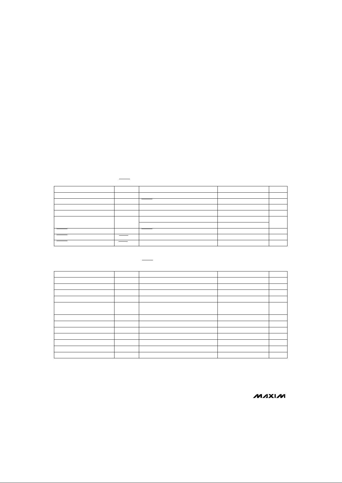
__________________Pin Configuration
MOD
LO+
LO-
MODULATION
BUFFER
LO INPUT
BUFFER
MIXER
VGC
VGC
OUT
BADJ
SHDN
POWER
AMPLIFIER
MASTER BIAS
________________Functional Diagram
19-0392; Rev 1; 5/96
PART
MAX2402EAP* -40°C to +85°C
TEMP. RANGE PIN-PACKAGE
20 SSOP
EVALUATION KIT MANUAL
FOLLOWS DATA SHEET
______________Ordering Information
* An alternate marking, MAX2402CAP, has been identically tested.
For free samples & the latest literature: http://www.maxim-ic.com, or phone 1-800-998-8800
MAX2402
800MHz to 1000MHz Transmitter
2 _______________________________________________________________________________________
ABSOLUTE MAXIMUM RATINGS
DC ELECTRICAL CHARACTERISTICS
(VCC= 4.75V to 5.5V, BADJ = open, SHDN = VCC- 0.5V, VGC = VCC, MOD = open, TA= -40°C to +85°C, unless otherwise noted.)
AC ELECTRICAL CHARACTERISTICS
(MAX2402 evaluation kit, VCC= 5.0V, BADJ = 2V, SHDN = VCC, MOD = 0V, VGC = VCC, R
LOAD
= 35Ω, fLO= 900MHz,
LO power = -3dBm, TA= -40°C to +85°C, unless otherwise noted.)
Stresses beyond those listed under “Absolute Maximum Ratings” may cause permanent damage to the device. These are stress ratings only, and functional
operation of the device at these or any other conditions beyond those indicated in the operational sections of the specifications is not implied. Exposure to
absolute maximum rating conditions for extended periods may affect device reliability.
Note 1: See
Typical Operating Characteristics
graphs.
Note 2: Guaranteed by design.
V
CC
........................................................................-0.3V to +6.5V
Continuous Power Dissipation (T
A
= +70°C)
SSOP (derate 16.7mW/°C above +70°C) ......................1.33W
Operating Temperature Range ...........................-40°C to +85°C
Storage Temperature Range.............................-65°C to +160°C
Lead Temperature (soldering, 10sec).............................+300°C
SHDN
= 0.5V
Not transmitting
SHDN = V
CC
VGC = V
CC
MOD = V
CC
MOD = 0V
CONDITIONS
µA0.15 2I
CCPD
Shutdown Supply Current
mA105I
CC
Supply Current
VV
CC
- 0.5V
SHDN
HighSHDN High Threshold
V0.5V
SHDN
LowSHDN Low Threshold
µA10.5I
PD
SHDN Bias Current
V4.75 5.50V
CC
Supply Voltage Range
µA115I
VGC
VGC Input Bias Current
µA
325
I
MOD
MOD Bias Current
-320
UNITSMIN TYP MAXSYMBOLPARAMETER
fLO= 900MHz + 901MHz
(Note 1)
(Note 1)
MOD = 5Vp-p @ 100kHz
(Note 2)
(Note 2)
(Note 2)
For max power out (50Ω input term)
(Note 2)
VGC = 0V (Note 1)
(Note 1)
CONDITIONS
dBm28.4IP3Output IP3 (BADJ = 1.0V)
dBC25HS33rd Harmonic Suppression
dBC22HS22nd Harmonic Suppression
dBC30CSCarrier Suppression
V1.0 2.5VGCVGC Control Range
MHz25MODBWMOD Usable Bandwidth
MHz800 1000f
LO
LO Frequency Range
dBm
dB24P
GAIN
Power Gain from LO
dBm-19P
MIN
Minimum Output Power
dBm21P
MAX
Maximum Output Power
UNITSMIN TYP MAXSYMBOLPARAMETER
P
OUT
= 20dBm (including current to load) mA165I
CCAC
Supply Current
-6 6P
LO
LO Input Power Range

MAX2402
800MHz to 1000MHz Transmitter
_______________________________________________________________________________________
3
25
20
-25
1.0 2.5
OUTPUT POWER vs.
GAIN CONTROL VOLTAGE
15
10
0
-10
-20
MAX2402 TOC 1
VGC (V)
OUTPUT POWER (dBm)
-5
-15
1.5
5
2.0
25
23
800 820 840 880 900 940 980
OUTPUT POWER vs. FREQUENCY
vs. TEMPERATURE
21
19
15
MAX2402 TOC 2
FREQUENCY (MHz)
OUTPUT POWER (dBm)
860
17
920 960
+85°C
+24°C
-40°C
22.0
-50 -30 -10 30 90
OUTPUT POWER vs.
TEMPERATURE
21.5
21.0
20.0
MAX2402 TOC 3
TEMPERATURE (°C)
OUTPUT POWER (dBm)
20.5
10 50 70
900MHz INPUT
25
23
21
012 4
OUTPUT POWER vs. BIAS CONTROL VOLTAGE
vs. FREQUENCY
19
17
15
13
7
MAX2402 TOC 4
BADJ VOLTAGE (V)
OUTPUT POWER (dBm)
11
9
35
800MHz
900MHz
990MHz
260
240
012 4
SUPPLY CURRENT vs. BIAS CONTROL VOLTAGE
vs. FREQUENCY
220
200
180
160
100
MAX2402 TOC 5
BADJ VOLTAGE (V)
SUPPLY CURRENT (mA)
140
120
35
800MHz
900MHz
990MHz
39
37
0.5 1.0 1.5 2.5
OUTPUT POWER LEVEL OF
2nd AND 3rd HARMONICS OF LO
(LO = 900MHz, -3dBm, MOD = 5V)
35
33
31
29
23
21
19
17
15
13
MAX2402 TOC 6
BADJ VOLTAGE (V)
OUTPUT POWER BELOW FUNDAMENTAL (dBC)
27
25
2.0 4.0
TA = -40°C
3.0 3.5
3rd HARMONIC
TA = +24°C
TA = +85°C
TA = -40°C
TA = +24°C
TA = +85°C
2nd HARMONIC
38
1.0 1.5 2.0 3.0
AMPLITUDE OF 3rd & 5th HARMONICS
OF MODULATED WAVEFORM
(100kHz SINEWAVE MODULATION OF 900MHz LO)
34
42
30
22
18
14
10
MAX2402 TOC 7
MODULATION VOLTAGE, PEAK-TO-PEAK (V)
OUTPUT POWER (dBC) BELOW 900.1MHz
26
2.5 5.0
TA = -40°C
3.5 4.0 4.5
900.5MHz
TA = +24°C
TA = +85°C
TA = -40°C
TA = +24°C
TA = +85°C
900.3MHz
__________________________________________Typical Operating Characteristics
(MAX2402 evaluation kit, VCC= 5.0V, BADJ = 2V, SHDN = VCC, MOD = 0V, VGC = VCC, R
LOAD
= 35Ω, fLO= 900MHz,
LO power = -3dBm)

_______________Detailed Description
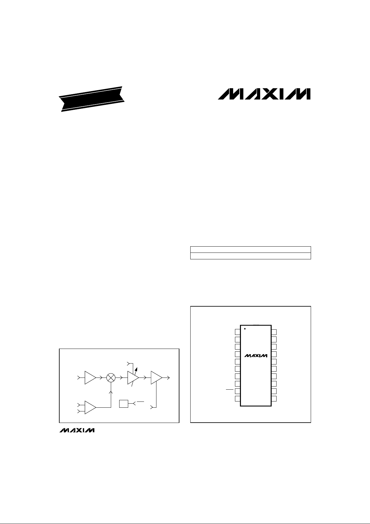
The MAX2402 transmitter is a versatile design that integrates several RF functions on a single IC. It has a wide
variety of applications in portable and stationary wireless designs. Each of the functional blocks (shown in
the
Functional Diagram
) is described in detail in the fol-
lowing sections.
LO Inputs
The LO inputs are internally capacitively coupled and
self biasing. The LO port can be driven differentially or
single ended. When terminated at the LO inputs with
50Ω, the transmitter will provide full output power for LO
inputs from -6dBm to +6dBm with single-ended drive,
and -12dBm to +6dBm with differential drive. Input
power beyond this range may saturate the LO input
buffer, while input power below this range may result in
less output power. The limiter is two cascaded differential stages, which also isolates the LO input from the
mixer. This will help reduce any frequency-pulling
effects in an external LO due to mixer loading. The limiter output drives one port of a double-balanced Gilbert
mixer.
MOD Input
The mixer’s other port, the MOD input, remains linear
over a 2V range from about 1.5V to 3.5V at the input.
When driven with digital modulation (0V to 5V), this port
will completely limit, resulting in a hard BPSKmodulated signal. Since this input is self biasing, carrier
suppression can be improved by externally capacitively
coupling the signal into the port (the MOD input resistance is approximately 10kΩ). This would compensate
for voltage offset or duty-cycle offset at this port, thus
increasing carrier suppression. This MOD self bias is
designed for very low on-chip offset, resulting in excellent carrier suppression. Since this port self biases
when the signal is removed from MOD, the mixer will
attenuate the output power by about 40dB, resulting in
further attenuation past that attained from VGC control—a useful feature for ASK modulation.
VGC Stage
The mixer output drives the VGC stage. This stage
attenuates through a multiplication technique that does
not distort the signal with increased attenuation. VGC
control is nonattenuating when connected to the V
CC
supply. VGC will attenuate for voltages from 2.5V to
1.0V. Most attenuation occurs between 1V and 2V.
Maximum attenuation is achieved below 0.8V. Typical
maximum attenuation is 40dB. At or beyond 40dB of
attenuation, the signal may be slightly nonmonotonic.
This means that there may be a slight upturn in the signal level at the low end of the VGC control range (typically about 1dB). Because of the stability implications,
we suggest that the user not plan on attenuating past
35dB within a feedback loop.
Power Amplifier
The VGC stage passes the signal to the power amplifier. This class AB stage will produce at least 20dBm of
output power for almost the complete transmit frequency range (with TA= +25°C). See
Typical Operating
Characteristics
.
BADJ Input
The BADJ input adjusts the bias of the output stage.
Increasing this voltage decreases bias current in the
output devices, which increases efficiency, but also
increases harmonic distortion (since the stage will be
pushed further toward class B operation). Decreasing
BADJ’s voltage increases bias current in the output
devices, resulting in higher output power and less harmonic distortion. Be sure to optimize BADJ for your
application.
MAX2402
800MHz to 1000MHz Transmitter
4 _______________________________________________________________________________________
_____________________Pin Description
NAME FUNCTION
1 VGC
Variable Gain Control Input.
Connect to VCCfor maximum gain.
2 MOD Baseband Modulation Input to mixer
PIN
3, 5, 8,
13, 15, 17,
18, 20
GND Ground
4, 12, 19 V
CC
Supply Voltage, set between 4.75V
and 5.5V
10 BADJ
Bias Adjustment Control for power
amplifier. Connect resistor from
BADJ to V+ or GND (see Table 1).
9 SHDN
Shutdown Control Input.
Low level = off, high level = on.
7 LO- Local-Oscillator Negative Input
6 LO+ Local-Oscillator Positive Input
14, 16 OUT Power-Amplifier Output
11 LGND
Connect 27nH inductor from LGND
to GND to maximize output power.

BADJ can be left open or adjusted with a single pullup or pull-down resistor to VCCor GND, respectively.
The value of this resistor determines the amount of
adjustment applied. A single resistor results in no current flow at BADJ during power-down (whereas a
resistor divider always has current flowing through the
resistors). Table 1 shows the approximate bias adjust
voltage at the pin for different resistor values. At lower
LO frequencies, where the transmitter gain and output
power is the highest, setting BADJ to a low voltage
(maximum bias current) causes excessive current in
the output and can cause unstable behavior in the IC.
At lower LO frequencies (around 800MHz), more than
22dBm of power is easily obtained with BADJ set for
3V or more. If higher bias current and less distortion is
desired in the 800MHz range, using a lower inductor
value on LGND (pin 11) (see the
Typical Application
Circuit
) might make the desired bias level stable. At
higher frequencies (near 1000MHz), a lower bias level
voltage results in more power (see the Output Power vs.
Bias Control Voltage vs. Frequency graph in the
Typical
Operating Characteristics
).
Power Amplifier Output
The power amplifier has an open-collector output that
can drive into a load of 30Ω to 50Ω; however, maximum
power transfer is obtained at about 35Ω. 27nH to
ground is recommended on LGND (pin 11), as shown
in the
Typical Application Circuit
. This inductor is used
as a current source on the base of the output stage to
pull stored charge out of the base.
SHDN Input
The SHDN input completely shuts down the current
from the supply and all signal pins when switched
below 0.5V. During normal operation, SHDN should
remain above VCC- 0.5V.
The shutdown control shuts down the total current to
below 150nA (typ). Power-up occurs within 10µs.
__________Applications Information
The MAX2402 transmitter operates within the 800MHz
to 1000MHz frequency range. Figure 1 shows a typical
application circuit. Additional applications information
can be obtained from the MAX2402 evaluation kit
manual.
MAX2402
800MHz to 1000MHz Transmitter
_______________________________________________________________________________________ 5
Resistor
Value (Ω)
BADJ with Resistor
Connected to GND (V)*
BADJ with Resistor
Connected to VCC(V)
10k 0.36 4.54
20k 0.63 4.27
30k 0.84 4.05
40k 1.00 3.89
50k 1.13 3.75
100k 1.54 3.34
200k 1.89 3.00
300k 2.05 2.85
400k 2.13 2.75
500k 2.20 2.68
1M 2.31 2.57
Figure 1. Typical Application Circuit
MAX2402
BADJ
300k
50Ω
39pF
50Ω
27nH
SHDN
GND
LO-
LO+
GND
V
CC
V
CC
GND
MOD
VGC
LGND
V
CC
GND
OUT
GND
VCO
MODULATION
SHUTDOWN
CONTROL
VARIABLE
GAIN CONTROL
OUT
GND
GND
V
CC
GND
39pF
47nH
V
CC
V
CC
39pF 0.01µF
V
CC
1
2
3
4
5
6
7
8
9
10
20
19
18
17
16
15
14
13
12
11
Table 1. Bias-Adjust Voltage for Various
Resistor Values
* Typical variation of BADJ over temperature and process is
less than 5%.

MAX2402
800MHz to 1000MHz Transmitter
6 _______________________________________________________________________________________
________________________________________________________Package Information
L
DIM
A
A1
B
C
D
E
e
H
L
α
MIN
0.068
0.002
0.010
0.005
0.278
0.205
0.301
0.022
0˚
MAX
0.078
0.008
0.015
0.009
0.289
0.212
0.311
0.037
8˚
MIN
1.73
0.05
0.25
0.13
7.07
5.20
7.65
0.55
0˚
MAX
1.99
0.21
0.38
0.22
7.33
5.38
7.90
0.95
8˚
INCHES MILLIMETERS
α
20-PIN SSOP
SHRINK
SMALL OUTLINE
PACKAGE
HE
D
A
A1
C
0.127mm
0.004in.
B
0.65 BSC0.0256 BSC
21-0003A
e
 Loading...