

Page 1

General Description
The MAX2385/MAX2386 evaluation kits (EV kits) simplify evaluation of the MAX2385/MAX2386. The EV kits
allow the evaluation of the CDMA and GPS low-noise
amplifiers (LNA), as well as the CDMA and GPS downconverter mixers, without the use of any additional support circuitry. The signal inputs and outputs use SMA
connectors to simplify the connection of RF test equipment.
The MAX2385/MAX2386 EV kits are assembled with an
associated IC and incorporate input and output matching components optimized for RF frequencies from
832MHz to 870MHz and an IF frequency of 110MHz.
Features
♦ +2.7V to +3.6V Operation
♦ 50Ω SMA Inputs and Outputs on RF, IF, and LO
Ports for Easy Testing
♦ All Matching Components Included
♦ Fully Assembled and Tested
Evaluate: MAX2385/MAX2386
MAX2385/MAX2386 Evaluation Kits
________________________________________________________________ Maxim Integrated Products 1
Component List
Ordering Information
19-2205; Rev 0; 10/01
For pricing, delivery, and ordering information, please contact Maxim/Dallas Direct! at
1-888-629-4642, or visit Maxim’s website at www.maxim-ic.com.
UCSP is a trademark of Maxim Integrated Products, Inc.
DESIGNATION QTY DESCRIPTION
1000pF ±10% ceramic capacitors
C1, C42 2
C3, C4, C39,
C40
C5, C6, C13,
C37, C38
C7, C8, C22,
C24, C30,
C34, C35
C9, C26 2
C12 1
C16, C23,
C29, C33
C19 1
C25, C32 2
(0402)
Murata GRM36X7R102K050A
7.0pF ±0.1pF ceramic capacitors
4
(0402)
Murata GRM36COG070B050A
0.5pF ±0.1pF ceramic capacitors
5
(0402)
Murata GRM36COG0R5B050A
100pF ±5% ceramic capacitors
7
(0402)
Murata GRM36COG101J050A
0.01µF 10% ceramic capacitors
(0402)
Murata GRM36X7R103K016A
3.0pF ±0.1pF ceramic capacitor
(0402)
Murata GRM36COG030B050A
6.8nF ±10% ceramic capacitors
4
Murata GRM36COG682B050A
2.2pF ±0.1pF ceramic capacitor
(0402)
Murata GRM36COG2R2B050A
2.0pF ±0.1pF ceramic capacitors
Murata GRM36COG020B050A
PART TEMP. RANGE IC PACKAGE
MAX2385EVKIT -40°C to +85°C5
MAX2386EVKIT -40°C to +85°C5 ✕ 4 UCSP™
DESIGNATION QTY DESCRIPTION
C27 1
C28 1
J1, J2, J3, J5,
J9, J11, J12
J4, J7, J10 3
JU1, JU2,
JU3, JU8
JU4–JU7 4
JU1–JU9 9
L2, L3, L10,
L11
L4 1
L5, L6 2
L7 1
L8 1
✕
4 UCSP™
22µF ±10% tantalum capacitor,
C case
AVX TAJC226K016
1.8pF ±0.1pF ceramic capacitor
(0402)
Murata GRM36COG1R8B050A
SMA edge mounts
7
EFJohnson 142-0701-801
SMA PC mounts
EFJohnson 142-0701-201
1 ✕ 2 headers (0.1in centers)
4
Digi-Key S1012-36-ND
✕
1
3 headers (0.1in centers)
Digi-Key S1012-36-ND
Shunts
Digi-Key S9000-ND
180nH 5% inductors
4
Toko 1608-FSR18J
2.7nH ±0.3nH inductor
Toko 1608-FS2N7S
5.6nH ±0.3nH inductors
Toko 1608-FS5N6S
22nH ±2% inductor
Murata LQW1608A22NG00
3.9nH ±0.3nH inductor
Toko 1608 FS3N9S
Page 2

Quick Start
The MAX2385/MAX2386 EV kits are fully assembled
and factory tested. Follow the instructions in the
Connections and Setup section for proper device evaluation.
Test Equipment Required
Table 1 lists the required test equipment to verify
MAX2385/MAX2386 operation. It is intended as a guide
only, and some substitutions are possible.
Connections and Setup
This section provides a step-by-step guide to operating
the EV kits and testing the devices’ functions. Ensure
that the shunts across jumpers ICLNA (JU1), IGLNA
(JU2), ICMIX (JU8), and IGMIX (JU3) are installed. Do
not turn on DC power or RF signal generators until all
connections are made.
Testing the Supply Current
1) Connect a DC supply set to +2.75V (through an
ammeter, if desired) to the V
CC
and GND terminals
on the EV kit. If available, set the current limit to
40mA. Do not turn on the supply.
2) Set the shunt across BUFF (JU7) to OFF. See Table
2 for positions of the shunts across G1, G2, and
MODE for the different modes of operation.
3) Turn on the DC supply; the supply current should
read approximately 0mA (shutdown mode), 9.6mA
(GPS mode, MAX2385), 16.9mA (GPS mode,
MAX2386), 3.7mA (ULG mode), 6.5mA (LG mode),
10.3mA (MG mode), 12.5mA (HGLL mode), and
17.4mA (HGHL mode).
4) Set the shunt across BUFF (JU7) to ON. This should
increase the current consumption in each mode by
5.2mA.
Testing the CDMA LNA
1) Connect a DC supply set to +2.75V (through an
ammeter if desired) to the V
CC
and GND terminals
on the EV kit. If available, set the current limit to
40mA. Do not turn on the supply.
2) See Table 2 for positions of the shunts across G1,
G2, and MODE for the different CDMA LNA modes.
3) Connect one RF signal generator to the CLNAIN
SMA connector. Do not turn on the generator’s output. Set the generator to an output frequency of
851MHz and set the generator power level to
-30dBm.
4) Connect the spectrum analyzer to the CLNAOUT
SMA connector. Set the spectrum analyzer to a center frequency of 851MHz and a total span of 10MHz.
5) Turn on the DC supply, then activate the RF generator’s output. An 851MHz signal shown on the spectrum analyzer display should indicate a magnitude of
approximately -15dBm (HGHL mode), -16dBm
(HGLL mode), -29dBm (MG mode), and -35dBm (LG
mode). Be sure to account for cable losses (between
0.5dB and 2dB) and circuit board losses (approximately 0.5dB) when computing gain and noise figure.
6) (Optional) Another method for determining gain is by
using a network analyzer. This has the advantage of
Evaluate: MAX2385/MAX2386
MAX2385/MAX2386 Evaluation Kits
2 _______________________________________________________________________________________
Component Suppliers
Component List (continued)
Table 1. Required Test Equipment
DESIGNATION QTY DESCRIPTION
R2, R3, R4,
VCC, GND,
L9 1
R10
R5 1 47.5kΩ ±1% resistor (0402)
R6, R7 2 69.8Ω ±1% resistors (0402)
R8 1 20kΩ ±1% resistor (0402)
T1, T2 2
U1 1
TP1
10nH ±2% inductor
Murata LQW1608A10NG00
40Ω ±1% resistors (0402)
Transformers
Macom ETC1-1T
MAX2385EBP/MAX2386EBP
✕
4 UCSP
5
Test points
3
Digi-Key 5000K-ND
SUPPLIER PHONE FAX
AVX 843-448-9411 843-448-1943
Murata 770-436-1300 770-436-3030
Toko 408-432-8281 408-943-9790
EQUIPMENT DESCRIPTION
RF Signal
Generators
RF Spectrum
Analyzer
Power Supply Capable of up to 40mA at +2.7V to +3.6V
Power Meter Capable of measuring up to 20dBm
Ammeter To measure supply current (optional)
Network
Analyzer
Capable of delivering at least 0dBm of
output power up to 1.6GHz (HP 8648C or
equivalent)
Capable of covering the operating
frequencies of the device, as well as a few
harmonics (HP 8561E or equivalent)
To measure small-signal return loss and
gain (optional, HP 8753D or equivalent)
Page 3

displaying gain over a swept frequency band, in
addition to displaying input and output return loss.
Refer to the network analyzer manufacturer’s user
manual for setup details.
Testing the GPS LNA
1) Connect a DC supply set to +2.75V (through an
ammeter, if desired) to the V
CC
and GND terminals
on the EV kit. If available, set the current limit to
40mA. Do not turn on the supply.
2) Set the shunt across MODE to HI, across G1 to LO,
and across G2 to HI. This places the device in GPS
mode (see Table 2).
3) Connect one RF signal generator to the GLNAIN
SMA connector. Do not turn on the generator’s output. Set the generator to an output frequency of
1575.42MHz and set the generator power level to
-30dBm.
4) Connect the spectrum analyzer to the GLNAOUT
SMA connector. Set the spectrum analyzer to a center frequency of 1575.42MHz and a total span of
10MHz.
5) Turn on the DC supply and activate the RF generator’s output. A 1575.42MHz signal shown on the
spectrum analyzer display should indicate a magnitude of approximately -12dBm (MAX2385) or -10dBm
(MAX2386). Be sure to account for cable losses
(between 0.5dB and 2dB) and circuit board losses
(approximately 0.5dB) when computing gain and
noise figure.
6) (Optional) Another method for determining gain is by
using a network analyzer. This has the advantage of
displaying gain over a swept frequency band, in
addition to displaying input and output return loss.
Refer to the network analyzer manufacturer’s user
manual for setup details.
Testing the CDMA Mixer
1) Connect a DC supply set to +2.75V (through an
ammeter if desired) to the VCCand GND terminals
on the EV kit. If available, set the current limit to
40mA. Do not turn on the supply.
2) See Table 2 for positions of the shunts across G1,
G2, and MODE for the different CDMA mixer modes.
3) Connect one RF signal generator to the LO_IN SMA
connector. Do not turn on the generator output. Set
the frequency to 1482MHz, and output power to
-10dBm. This is the LO signal.
4) Connect another RF signal generator to the CMIXIN
SMA connector. Do not turn on the generator output.
Set the signal generator to 851MHz and output
power level to -30dBm.
5) Connect the spectrum analyzer to the CIF SMA connector. Set the spectrum analyzer to a center frequency of 110MHz and a total span of 10MHz.
6) Turn on the DC supply and the signal generator outputs.
7) A 110MHz signal shown on the spectrum analyzer
display should indicate a magnitude of approximately
-19dBm (HGHL/HGLL mode), -19dBm (MG mode),
-20dBm (LG mode), or -27dBm (ULG mode). Be sure
to account for cable losses (between 0.5dB and 2dB)
and circuit board losses (approximately 0.5dB) when
computing gain and noise figure.
Evaluate: MAX2385/MAX2386
MAX2385/MAX2386 Evaluation Kits
_______________________________________________________________________________________ 3
Table 2. Mode Selection Truth Table
MODES
High Gain, High
Linearity (HGHL)
High Gain, Low
Linearity (HGLL)
Midgain (MG) 1 0 1 ——● ———● ——
Low Gain (LG) 1 1 1 —— ● ———● ——
Ultra-Low Gain
(ULG)
GPS 0 1 1 — ——— ● ———— ●
Shutdown
(SHDN)
CONTROL PINS
G1 G2 MODE HGHL HGLL MG LGHL GPS HG MG LG ULG GPS
00 1
11 0 —
10 0 ———
0X — — — — — ——————
● ————● ————
LNA MIXER
● —— —● ————
FUNCTION
● — ——— ● —
Page 4

Evaluate: MAX2385/MAX2386
Testing the GPS Mixer
1) Connect a DC supply set to +2.75V (through an
ammeter, if desired) to the VCCand GND terminals
on the EV kit. If available, set the current limit to
40mA. Do not turn on the supply.
2) Set the shunt across MODE to HI, across G1 to LO,
and across G2 to HI. This places the device in GPS
mode (see Table 2).
3) Connect one RF signal generator to the LO_IN SMA
connector. Do not turn on the generator output. Set
the frequency to 1465.42MHz, and output power to
-10dBm. This is the LO signal.
4) Connect another RF signal generator to the GMIXIN
SMA connector. Do not turn on the generator output.
Set the signal generator to 1575.42MHz and output
power level to -30dBm.
5) Connect the spectrum analyzer to the GIF SMA connector. Set the spectrum analyzer to a center frequency of 110MHz and a total span of 10MHz.
6) Turn on the DC supply and the signal generator outputs.
7) A 110MHz signal shown on the spectrum analyzer
display should indicate a magnitude of approximately -18dBm (MAX2385) or -17dBm (MAX2386). Be
sure to account for cable losses (between 0.5dB and
2dB) and circuit board losses (approximately 0.5dB)
when computing gain and noise figure.
Testing the LO Output Buffer
1) Connect a DC supply set to +2.75V (through an
ammeter, if desired) to the V
CC
and GND terminals
on the EV kit. If available, set the current limit to
40mA. Do not turn on the supply.
2) Set the shunt across jumper BUFF (JU7) to ON.
3) Connect one RF signal generator to the LO_IN SMA
connector. Do not turn on the generator output. Set
the frequency to 1482MHz, and output power to
-10dBm.
4) Connect the spectrum analyzer to the LO_OUT SMA
connector. Set the spectrum analyzer to a center frequency of 741MHz and a total span of 10MHz.
5) Turn on the DC supply and the signal generator outputs.
6) A 741MHz signal shown on the spectrum analyzer
display should indicate a magnitude of approximately
-14dBm. Be sure to account for cable losses
(between 0.5dB and 2dB), the 7.4dB 100Ω to 50Ω
matching pad, and circuit board losses (approximately 0.5dB) when computing gain and noise figure.
Layout
The EV kit’s PC board can serve as a guide for laying
out a circuit board using the MAX2385/MAX2386.
Keep RF signal lines as short as possible to minimize
losses and radiation. Always use controlled-impedance
lines on all high-frequency inputs and outputs and use
low-inductance connections to ground on all GND pins.
At the mixer outputs, keep the differential lines together
and of the same length to ensure signal balance.
MAX2385/MAX2386 Evaluation Kits
4 _______________________________________________________________________________________
Page 5

Evaluate: MAX2385/MAX2386
MAX2385/MAX2386 Evaluation Kits
_______________________________________________________________________________________ 5
Figure 1. MAX2385/2386 EV Kit Schematic
V
CC
JU3
21
IGMIX
5.6nH
C6
0.5pF
L5
5.6nH
C19
2.2pF
L7
22nH
C25
2.0pF
C37
0.5pF
180nH
A2
A4
B3
A3
L6
A1
B1
B2
C1
D1
TP1
GIF+
GLNAOUT
CLNAOUT
G1
GLNAIN
GND
C2
RBIAS
R5
47.5kΩ
GIF-
MAX2385
CLNAING2VCCGND
D2C3D3
MODE
U1
GMIXIN
C27
22µF
A5
CMIXIN
LO_OUT
LO_IN
D4
GND
CIF+
CIF-
B5
C4
B4
C5
D5
C34
100pF
C26
0.01µF
L11
L10
180nH
20kΩ
V
CC
L2
1
C4
7.0pF
2
3
C3
7.0pF
V
CC
JU2
21
IGLNA
JU1
21
ICLNA
JU5
L8
3.9nH
L9
10nH
INDO603
C5
0.5pF
V
HI
G1
LO
180nHL3180nH
L4
2.7nH
R3
0Ω
C22
100pF
CC
R4
1
0Ω
2
3
C8
100pFC90.01µF
C7
100pF
C1
1000pF
J3
C13
0.5pF
J2
C12
3pF
J1
C29
6.8nF
J5
C33
6.8nF
J9
T1
5
4
V
CC
C28
1.8pF
C32
2pF
V
CC
R2
0Ω
C38
0.5pF
7.0pF
7.0pF
R8
J6
J8
R10
0Ω
JU4
1
HI
2
MODE
LO
3
C16
6.8nF
J4
C23
6.8nF
J7
V
CC
JU8
21
ICMIX
C35
100pF
C42
69.8Ω
C30
100pF
1000pF
R7
69.8Ω
J11
J12
J10
5
4
R6
T2
1
C39
2
3
C40
C24
100pF
V
CC
JU7
1
ON
2
BUFF
OFF
3
V
CC
JU6
1
HI
2
G2
LO
3
Page 6

Evaluate: MAX2385/MAX2386
MAX2385/MAX2386 Evaluation Kits
6 _______________________________________________________________________________________
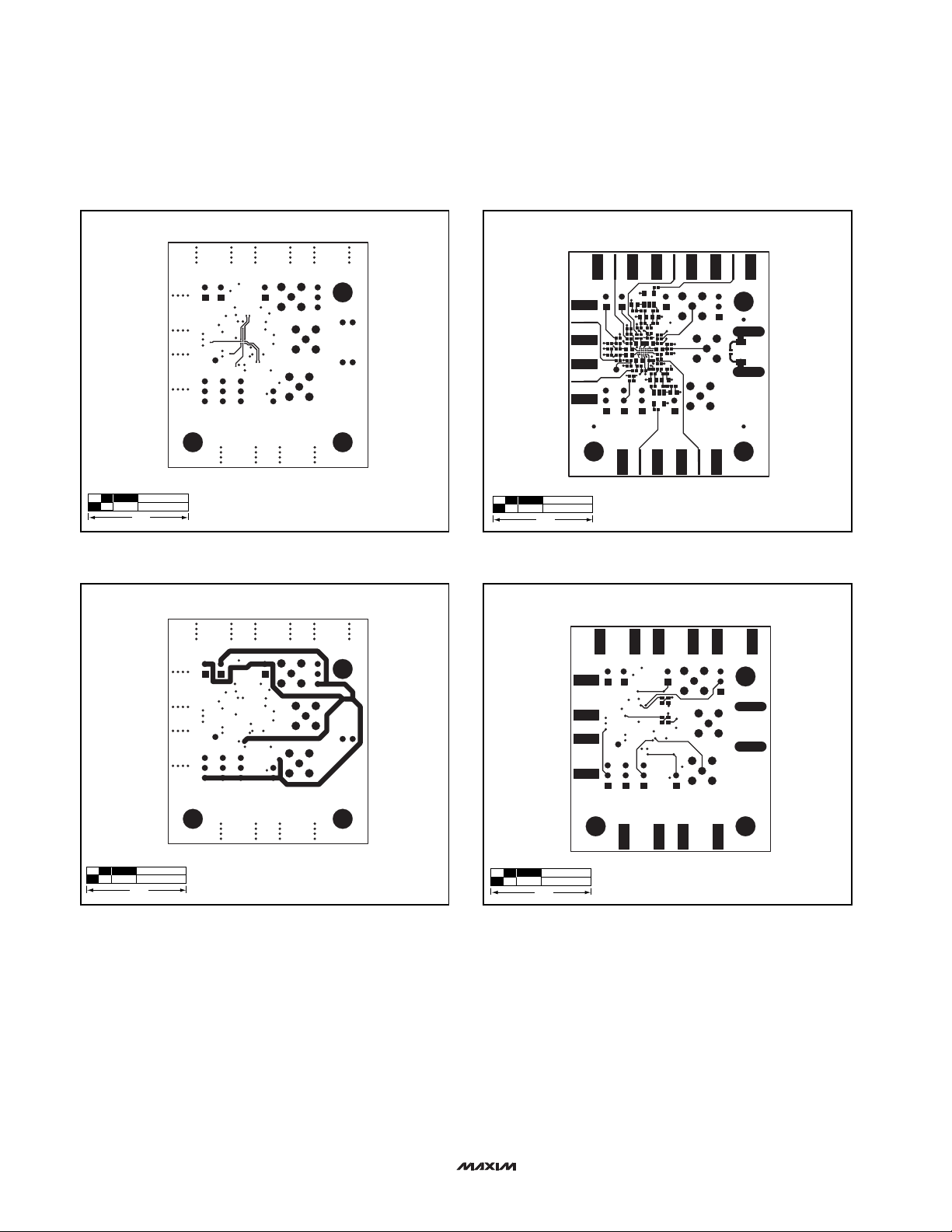
Figure 2. MAX2385/MAX2386 EV Kit Component Placement
Guide—Component Side
Figure 3. MAX2385/MAX2386 EV Kit Component Placement
Guide—Solder Side
Figure 4. MAX2385/MAX2386 EV Kit PC Board Layout—Ground
Plane 1
Figure 5. MAX2385/MAX2386 EV Kit PC Board
Layout—Component Side
1.0"
1.0"
1.0"
1.0"
Page 7
Evaluate: MAX2385/MAX2386
MAX2385/MAX2386 Evaluation Kits
Maxim cannot assume responsibility for use of any circuitry other than circuitry entirely embodied in a Maxim product. No circuit patent licenses are
implied. Maxim reserves the right to change the circuitry and specifications without notice at any time.
Maxim Integrated Products, 120 San Gabriel Drive, Sunnyvale, CA 94086 408-737-7600 _____________________ 7
© 2001 Maxim Integrated Products Printed USA is a registered trademark of Maxim Integrated Products.
Figure 6. MAX2385/MAX2386 EV Kit PC Board Layout
Figure 7. MAX2385/MAX2386 EV Kit PC Board Layout
Figure 8. MAX2385/MAX2386 EV Kit PC Board Layout—
Component Side
Figure 9. MAX2385/MAX2386 EV Kit PC Board Layout—Solder
Side
1.0"
1.0"
1.0"
1.0"
 Loading...