

Page 1
General Description
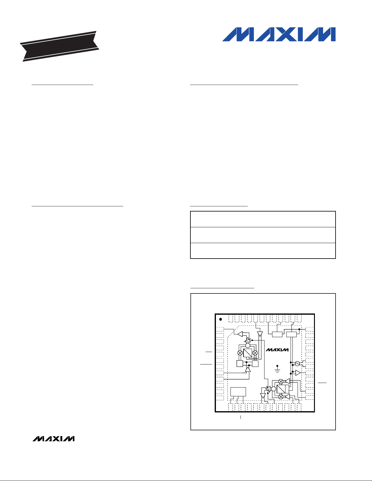
The MAX2370 integrated quadrature transmitter is
designed for 450MHz applications. The device takes a
differential I/Q baseband input and converts it up to
intermediate frequency (IF) through a quadrature modulator and IF variable-gain amplifier (VGA). The signal is
then routed to an external IF filter and upconverted to RF
through an image-reject mixer and RF VGA. The signal
is further amplified with an on-chip power amplifier (PA)
driver. An IF synthesizer, an RF synthesizer, a local
oscillator buffer, and an SPI™/QSPI™/MICROWIRE™compatible, 3-wire programmable bus complete the
basic functional blocks of this IC.
The MAX2370 is available in a 48-pin TQFN package
with exposed paddle and is specified for the extended
temperature range (-40°C to +85°C).
Applications
450MHz CDMA/WCDMA Phones
OFDM, cdma2000®, WCDMA, NMT
Wireless Data Links
Features
♦ 450MHz Operating Frequency
♦ +8dBm Output Power
-64dBc Typical ACPR at ±885kHz Offset
-66dBc Typical ACPR at ±1.125MHz Offset
♦ 100dB Power-Control Range
♦ Dual Synthesizer for RF and IF Local Oscillators
♦ SPI/QSPI/MICROWIRE-Compatible 3-Wire
Interface Bus
♦ Single-Sideband Upconverter
♦ Directly Drives External Power Amplifier
MAX2370
Complete 450MHz Quadrature Transmitter
________________________________________________________________ Maxim Integrated Products 1
Ordering Information
19-0222; Rev 0; 5/05
For pricing, delivery, and ordering information, please contact Maxim/Dallas Direct! at
1-888-629-4642, or visit Maxim’s website at www.maxim-ic.com.
EVALUATION KIT
AVAILABLE
PART
TEMP RANGE
PIN-PACKAGE
PKG
CODE
MAX2370ETM
(7mm x 7mm)
T4877-3
MAX2370ETM+
(7mm x 7mm)
T4877+3
SPI and QSPI are trademarks of Motorola, Inc.
MICROWIRE is a trademark of National Semiconductor Corp.
cdma2000 is a registered trademark of Telecommunications
Industry Association.
*EP = Exposed paddle.
+Denotes lead-free package.
REF
N.C.
N.C.
N.C.
IFLO
V
CC
I+
I-
TANK+
TANK-
N.C.
LOCK
V
CCDRV
V
CC
IFIN+
IFIN-
RBIAS
N.C.
N.C.
N.C.
RFOUT
1
2
3
4
5
6
7
8
9
10
11
12
36
35
34
33
32
31
30
29
28
27
26
25
N.C.
IFOUT-
IFOUT+
V
CC
Q-
Q+
V
CC
N.C.
DI
CLK
N.C.
GND
GNDLON.C.
RFPLL
V
CCRFCP
RFCP
VCCV
CCIFCP
IFCP
GND
GC
4847464544434241403938
37
1314151617181920212223
24
CS
SHDN
IDLE
TXGATE
TOP VIEW
MAX2370
+45 -45
90°
0°
IF PLLRF PLL
Σ
Σ
SPI
INTERFACE
EP
/2
90°
0°
Pin Configuration/
Functional Diagram
-40°C to +85°C
-40°C to +85°C
48 Thin QFN-EP*
48 Thin QFN-EP*
Page 2
MAX2370
Complete 450MHz Quadrature Transmitter
2 _______________________________________________________________________________________
ABSOLUTE MAXIMUM RATINGS
Stresses beyond those listed under “Absolute Maximum Ratings” may cause permanent damage to the device. These are stress ratings only, and functional
operation of the device at these or any other conditions beyond those indicated in the operational sections of the specifications is not implied. Exposure to
absolute maximum rating conditions for extended periods may affect device reliability.
VCC, RFOUT, V
CCIFCP
, V
CCRFCP
,
V
CCDRV
to GND.................................................-0.3V to +3.6V
DI, SCLK,
CS, GC, SHDN, TXGATE, IDLE,
LOCK to GND.........................................-0.3V to (V
CC
+ 0.3V)
AC Input Pins (IFIN_, Q_, I_, TANK_, REF,
RFPLL, LO) to GND.....................................................1V Peak
Digital Input Current (SHDN, TXGATE, IDLE,
SCLK, DI, CS) ...............................................................±10mA
Continuous Power Dissipation (T
A
= +70°C)
48-Pin Thin QFN (derate 38.5mW/°C above +70°C).....3077mW
Operating Temperature Range ...........................-40°C to +85°C
Junction Temperature......................................................+150°C
Storage Temperature Range .............................-65°C to +150°C
Lead Temperature (soldering, 10s) .................................+300°C
DC ELECTRICAL CHARACTERISTICS
(VCC= +2.7V to +3.3V, SHDN = IDLE = TXGATE = high, VGC= 2.5V, R
BIAS
= 10kΩ, registers set according to Table 1, f
REF
=
19.2MHz, no AC signals applied, T
A
= -40°C to +85°C. Typical values are at VCC= +3.0V, TA= +25°C, unless otherwise noted.)
(Note 1)
PARAMETER CONDITIONS
UNITS
Supply Voltage Range V
CC
2.7 3.3 V
VGC = 0.6V 53 79
VGC = 1.95V 57 87
P
RFOUT
= +5.5dBm, IFG[2:0] = 011 118
P
RFOUT
= +8dBm, IFG[2:0] = 011 134
Addition for IFLO buffer 3.4 7.7
IDLE = low 6 10
Operating Supply Current
TXGATE = low 5 7
mA
Sleep-Mode Supply Current SHDN = 0V 0.5 20 µA
Logic-High Voltage
V
Logic-Low Voltage
V
Logic Input Current -5 +5 µA
GC Input Current VGC = 0.5V to 2.5V 3.3 5 µA
GC Input Current During Shutdown SHDN = low, VGC = 2.5V 7 11 µA
Lock Indicator High Voltage (Locked) 47kΩ pullup load
V
CC
V
Lock Indicator Low Voltage (Unlocked)
47kΩ pullup load 0.5 V
CAUTION! ESD SENSITIVE DEVICE
MIN TYP MAX
0.7 x V
CC
0.3 x V
0.4V
CC
Page 3
MAX2370
Complete 450MHz Quadrature Transmitter
_______________________________________________________________________________________ 3
AC ELECTRICAL CHARACTERISTICS
(MAX2370 EV kit, VCC= +2.7V to +3.3V, SHDN = IDLE = TXGATE = high, VGC= 2.5V, R
BIAS
= 10kΩ, 50Ω system, TA= -40°C to
+85°C. Typical values are at V
CC_
= SHDN = IDLE = TXGATE = CS = 3.0V, f
REF
= 19.2MHz, LO input power = -15dBm, fLO= 575MHz,
f
RFOUT
= 455MHz, fIF= 120MHz, registers set according to Table 1, input voltage at I and Q = 130mV
RMS
differential,
cascade specifications assume 400Ω IF filter with 5dB insertion loss, T
A
= +25°C, unless otherwise noted.) (Note 1)
PARAMETER CONDITIONS
MIN
TYP
MAX
UNITS
MODULATOR
IF Frequency Range
Typically meets 30dB sideband suppression over this
frequency range
95 to 195
MHz
I/Q Common-Mode Input Voltage
(Notes 2, 3)
VCC -
V
I/Q Input Current VCM = 1.4V 6 µA
+25°C < TA < +85°C7087
Gain-Control Range
TA = -40°C85
dB
Gain Variation Over Temperature
Relative to +25°C, TA = -40°C to +85°C -2.4, +3.4 dB
Carrier Suppression VGC = 2.5V 30 40 dB
Sideband Suppression VGC = 2.5V 30 40 dB
IF Output Noise at Rx Band
V
GC
set to give -12dBm IF output power, noise
measured at 10MHz offset (Note 4)
dBm/Hz
f
OFFSET
= ±885kHz in 30kHz BW -66
-69
f
OFFSET
= ±1.98MHz in 30kHz BW -84
IF Adjacent Channel Power Ratio
IS-95 Reverse Modulation
V
GC
set to give
-12dBm IF output
power, IFG[2:0] =
011
f
OFFSET
= ±4MHz in 30kHz BW -89
dBc
UPCONVERTER AND PREDRIVER
RFOUT Frequency Range
See the Typical Operating Characteristics for typical gain
vs. frequency
410 to 500
MHz
LO Frequency Range
530 to 695
MHz
LO and RFPLL Input Power -15 -7 0
dBm
Conversion Gain 23 dB
MPL Gain Change MPL = 0, gain relative to MPL = 1
dB
+25°C < TA < +85°C3044
RF Gain-Control Range
TA = -40°C46
dB
RF Image Suppression At maximum output power -20 dBc
Rx Band Noise Power
P
RFOUT
= +8dBm, noise measured at +10MHz offset
(Note 4)
dBm/Hz
CASCADED MODULATOR, UPCONVERTER, AND PREDRIVER
RFOUT Output Power Meets ACPR specifications (Note 4) 5.5 10
dBm
f
OFFSET
= ±885kHz in 30kHz BW -64 -57
-66 -61
f
OFFSET
= ±1.98MHz in 30kHz BW -82 -78
P
OU T
= + 8d Bm ,
IFG[2:0] = 011
f
OFFSET
= ±4MHz in 30kHz BW -86 -78
f
OFFSET
= ±885kHz in 30kHz BW -64 -58
-67 -62
f
OFFSET
= ±1.98MHz in 30kHz BW -81 -78
Ad j acent C hannel P ow er Rati o
IS - 95 Rever se M od ul ati on ( N ote 4)
P
OUT
= +5.5dBm,
IFG[2:0] = 011
f
OFFSET
= ±4MHz in 30kHz BW -86 -85
dBc
VGC = 0.5V to 2.5V
f
= ±1.125MHz in 30kHz BW
OFFSET
Typically meets 30dB image suppression over this range
VGC = 0.5V to 2.5V
f
= ±1.125MHz in 30kHz BW
OFFSET
f
= ±1.125MHz in 30kHz BW
OFFSET
1.35
-138 -135
-3.4
-130 -128.5
1.25
Page 4
MAX2370
Complete 450MHz Quadrature Transmitter
4 _______________________________________________________________________________________
Note 1: Guaranteed by production test at TA= +25°C to +85°C, design and characterization at TA= -40°C.
Note 2: ACPR is met over the specified V
CM
range.
Note 3: V
CM
must be supplied by the I/Q baseband source with ±8µA current capability.
Note 4: Guaranteed by design and characterization to 6σ.
Note 5: When enabled with RCP_TURBO1 and RCP_TURBO2 (see Tables 3 and 4), the total charge-pump current is specified.
For all values of RCP, the total turbolock current is 1.63 times the corresponding nonturbo current value.
AC ELECTRICAL CHARACTERISTICS (continued)
(MAX2370 EV kit, VCC= +2.7V to +3.3V, SHDN = IDLE = TXGATE = high, VGC= 2.5V, R
BIAS
= 10kΩ, 50Ω system, TA= -40°C to
+85°C. Typical values are at V
CC_
= SHDN = IDLE = TXGATE = CS = 3.0V, f
REF
= 19.2MHz, LO input power = -15dBm, fLO= 575MHz,
f
RFOUT
= 455MHz, fIF= 120MHz, registers set according to Table 1, input voltage at I and Q = 130mV
RMS
differential,
cascade specifications assume 400Ω IF filter with 5dB insertion loss, T
A
= +25°C, unless otherwise noted.) (Note 1)
PARAMETER CONDITIONS
UNITS
Output Power Variation Over
Temperature
Relative to +25°C, T
A
= -40°C to +85°C
dB
IF PLL
Reference Frequency 530
MHz
Refer ence Fr eq uency S i g nal Level 0.1 0.6
V
P-P
IF Main-Divide Ratio 256
IF Reference-Divide Ratio 2
VCO Operating Range 190 to 390
MHz
ICP = 00 96 139 174
ICP = 01 135 192 240
ICP = 10 190 278 348
Charge-Pump Source/Sink
Current
ICP = 11 267 390 488
µA
Turbolock Boost Current ICP = 11, ICP_MAX = 1 533 774 968 µA
Charge-Pump Source/Sink
Current Matching
All values of ICP, over compliance range 6 %
IF Charge-Pump Compliance 0.5
V
C C I FC P
-
0.5V
V
RF PLL
RF PLL Frequency Range RF PLL operated at 2x LO frequency
MHz
Reference Frequency 530
MHz
RF Main-Divide Ratio
RF Reference-Divide Ratio 2
RCP = 00 220 325 406
RCP = 01 441 650 813
RCP = 10 499 738 923
Charge-Pump Source/Sink
Current
RCP = 11 717
µA
Turbolock Boost Current (Note 5)
µA
Charge-Pump Source/Sink
Current Matching
All values of RCP, over compliance range 6 %
RF Charge-Pump Compliance 0.5
V
C C R FC P
-
0.5V
V
Phase-Detector Noise Floor
RCP = 11, RCP_TURBO1 = RCP_TURBO2 = 0, 50kHz
comparison frequency
dBc/Hz
MIN TYP MAX
0, -2
16,383
2047
4096 262,143
1063 1329
1152 1694 2118
-162
1300
8191
Page 5
MAX2370
Complete 450MHz Quadrature Transmitter
_______________________________________________________________________________________ 5
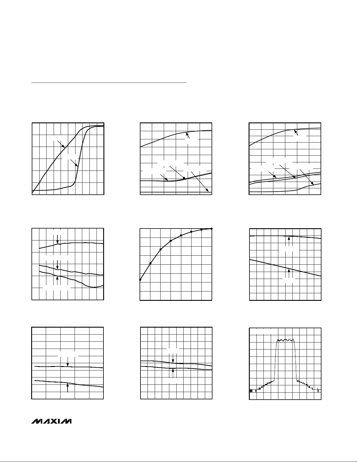
Typical Operating Characteristics
(MAX2370 EV kit, V
CC_
= SHDN = IDLE = TXGATE = CS = 3.0V, f
REF
= 19.2MHz, LO input power = -15dBm, fLO= 575MHz, f
RFOUT
=
455MHz, f
IF
= 120MHz, R
BIAS
= 10kΩ, VGC= 2.5V, registers set according to Table 1, input voltage at I and Q = 130mV
RMS
differential,
TA= +25°C, unless otherwise noted.)
-100
-40
-60
-80
-20
0
20
1.0 1.81.61.2 1.4 2.0 2.2 2.4 2.6 2.8 3.0
RF OUTPUT POWER AND SUPPLY CURRENT
vs. GAIN-CONTROL VOLTAGE
MAX2370 toc01
V
GC
(V)
RF OUTPUT POWER (dBm)
50
110
90
70
130
150
170
SUPPLY CURRENT (mA)
POWER
CURRENT
-90
-70
-80
-40
-50
-60
-10
-20
-30
0
2.1 2.32.2 2.4 2.5 2.6 2.7
IF OUTPUT POWER AND IF ACPR
vs. GAIN-CONTROL VOLTAGE
MAX2370 toc02
VGC (V)
IF OUTPUT POWER AND IF ACPR (dBm, dBc)
POWER
ACPR ±885kHz
ACPR ±1.125MHz
ACPR ±1.98MHz
-90
-80
-70
-60
-50
-40
-30
-20
-10
0
10
20
2.1 2.2 2.3 2.4 2.5 2.6 2.7
RF OUTPUT POWER AND RF ACPR
vs. GAIN-CONTROL VOLTAGE
MAX2370 toc03
VGC (V)
RF OUTPUT POWER AND RF ACPR (dBm/dBc)
POWER
ACPR ±885kHz
ACPR ±1.125MHz
ACPR ±1.98MHz
0
15
10
5
20
25
30
400 440430410 420 450 460 470 480 490 500
RF GAIN, IMAGE SUPPRESSION, AND LO
SUPPRESSION vs. FREQUENCY
MAX2370 toc04
RF FREQUENCY (MHz)
RF GAIN (dB)
-60
-30
-40
-50
-20
-10
0
SUPPRESSION (dBc)
LO SUPPRESSION
IMAGE SUPPRESSION
GAIN
NORMALIZED IF OUTPUT POWER vs. IFG[2:0]
MAX2370 toc05
-16
-14
-10
-12
-4
-2
-6
-8
0
NORMALIZED IF OUTPUT POWER (dB)
0231
4
567
IFG[2:0] (DECIMAL)
0
0.2
0.1
0.4
0.3
0.6
0.5
0.7
0.9
0.8
1.0
400 420 430 440410 450 460 470 490480 500
RFOUT PORT S22
MAX2370 toc06
FREQUENCY (MHz)
S22 MAGNITUDE
-100
-80
-90
-60
-70
-40
-50
-30
-10
-20
0
S22 PHASE (°)
MAGNITUDE
PHASE
0
0.2
0.1
0.4
0.3
0.6
0.5
0.7
0.9
0.8
1.0
1050 1100 1150 1200 1250 1300
RFPLL PORT S11
MAX2370 toc07
FREQUENCY (MHz)
S11 MAGNITUDE
-100
-80
-90
-60
-70
-40
-50
-30
-10
-20
0
S11 PHASE (°)
MAGNITUDE
PHASE
0
0.2
0.1
0.4
0.3
0.6
0.5
0.7
0.9
0.8
1.0
500 540 560 580520 600 620 640 680660 700
LO PORT S11
MAX2370 toc08
FREQUENCY (MHz)
S11 MAGNITUDE
-100
-80
-90
-60
-70
-40
-50
-30
-10
-20
0
S11 PHASE (°)
MAGNITUDE
PHASE
-100
-110
-80
-90
-60
-70
-40
-50
-30
-10
-20
FREQUENCY
IF OUTPUT SPECTRUM
MAX2370 toc9
POWER (dBm)
CENTER: 120MHz, SPAN: 5MHz, RBW: 30kHz
P
OUT
= -12dBm
Page 6
MAX2370
Complete 450MHz Quadrature Transmitter
6 _______________________________________________________________________________________
Pin Description
PIN NAME FUNCTION
1 RFOUT
Transmitter RF Output. This open-collector output requires a pullup inductor to the supply voltage,
which can be part of the output matching network.
2, 10, 11, 16,
17, 32–35,
43, 47
N.C. No Connection. Leave these pins open-circuit. Some of these pins are internally connected.
3LOCK
Open-Drain Output Indicating LOCK Status of the IF and/or the RF PLLs. Requires an external
pullup resistor. Control using configuration register bits LD_MODE[1:0].
4V
CCDRV
Power Supply for the RF Driver Stage. Bypass to PC board ground with a capacitor placed as
close to the pin as possible. Do not share capacitor ground vias with other ground connections.
5 IDLE
Digital Input. Drive to logic-high for normal operation. Logic-low on IDLE shuts down everything
except the RF PLL. A small RC lowpass filter can be used to filter digital noise.
6V
CC
Power Supply for the Upconverter Stage. Bypass to PC board ground with a capacitor placed as
close to the pin as possible. Do not share capacitor ground vias with other ground connections.
7 TXGATE
D i g i tal Inp ut. D r i ve to logic-high for nor m al op er ati on. Logic-low on TXG ATE shuts d ow n ever ythi ng
excep t the RF P LL, IF P LL, IF V C O. A sm al l RC l ow p ass can b e used to fi l ter d i g i tal noi se.
8, 9 IFIN+, IFIN-
Differential IF Inputs to the RF Upconverter. IFIN+ and IFIN- are internally biased to typically V
CC
-
1.5V. The input impedance for this port is nominally 400Ω differential. AC-couple the output of the
differential IF filter to this port. Keep the differential lines as short as possible to minimize the
effects of stray pickup.
12 RBIAS
Bias Resistor Connection. Internally biased to typically 1.18V. An external resistor must be
connected from RBIAS to ground to set the bias current for the upconverters and PA driver
stages. The nominal resistor value is 10kΩ. This value can be altered to optimize the linearity of
the driver stage.
Typical Operating Characteristics (continued)
(MAX2370 EV kit, V
CC_
= SHDN = IDLE = TXGATE = CS = 3.0V, f
REF
= 19.2MHz, LO input power = -15dBm, fLO= 575MHz, f
RFOUT
=
455MHz, f
IF
= 120MHz, R
BIAS
= 10kΩ, VGC= 2.5V, registers set according to Table 1, input voltage at I and Q = 130mV
RMS
differential,
TA= +25°C, unless otherwise noted.)
-90
-70
-80
-50
-60
-30
-40
-20
0
-10
10
FREQUENCY
RF OUTPUT SPECTRUM
MAX2370 toc10
POWER (dBm)
P
OUT
= +8dBm
CENTER: 455MHz, SPAN: 5MHz, RBW: 30kHz
-100
-80
-90
-60
-70
-50
-40
-20
-30
-10
239.8 239.9 240.0 240.1 240.2 240.3
IF LOCAL OSCILLATOR SPECTRUM
MAX2370 toc11
FREQUENCY (MHz)
IF LO POWER (dBm)
P
REF
= -10dBm
Page 7

MAX2370
Complete 450MHz Quadrature Transmitter
_______________________________________________________________________________________ 7
Pin Description (continued)
PIN NAME FUNCTION
13, 14, 15
CLK, DI, CS
CMOS Inputs from the 3-Wire Serial Bus (SPI/QSPI/MICROWIRE Compatible). A small RC
lowpass filter on each of these pins can be used to reduce noise on these lines.
18, 19
Differential IF Outputs. This port is active when IF_SEL is LOW and supports both FM and CDMA
modes. IFOUT+ and IFOUT- must be inductively pulled up to V
CC
and differentially loaded with
typically 560Ω. A 400Ω differential IF bandpass filter is connected between this port and IFIN+/-.
The pullup inductors can be part of the filter structure. The differential output impedance of this
port is nominally 400Ω, including the 560Ω external differential resistor. Keep the transmission
lines from these pins as short as possible to minimize the unintentional pickup of spurious signals
and noise.
20 GC
RF and IF Gain-Control Analog Input. Accepts input voltages from 0.5V (minimum gain) to 2.5V
(maximum gain). When not driven, GC is internally biased to typically 1.5V. RC lowpass filter the
voltage applied to this pin to remove DAC noise or PDM clock spurs.
21 V
CC
Power Supply for the IF VGA. Bypass to PC board ground with a 0.1µF capacitor placed as close
to the pin as possible. Do not share capacitor ground vias with other ground connections.
22 V
CC
Power Supply for the I/Q Modulator. Bypass to PC board ground with a 0.1µF capacitor placed as
close to the pin as possible. Do not share capacitor ground vias with other ground connections.
23, 24 Q+, Q-
Differential Q-Channel Baseband Inputs to the Modulator. Q+ and Q- connect directly to the
bases of a differential pair and require a typical 1.35V to (V
CC
- 1.5V) external common-mode bias
voltage.
25, 26 I+, I-
Differential I-Channel Baseband Inputs to the Modulator. I+ and I- connect directly to the bases of
a differential pair and require a typical 1.35V to (VCC - 1.5V) external common-mode bias voltage.
27 SHDN
Digital Input. Drive LOW to shut down the entire IC, drive high for normal operation. A small RC
lowpass filter can be used to filter digital noise.
28 V
CC
Power Supply for the VCO Section. Bypass to PC board ground with a 0.1µF capacitor placed as
close to the pin as possible. Do not share capacitor ground vias with other ground connections.
29 IFLO
IF LO O utp ut. P r ovi d es access to the IF V C O outp ut and can b e used to d r i ve an exter nal P LL. It can
b e d i sab l ed b y l og i c- l ow on the BU F_E N contr ol b i t. IFLO i s i nter nal l y b i ased to typ i cal l y 1.5V .
30, 31
Differential Tank Connections for the IF VCO. TANK+ and TANK- are internally biased to
approximately 1.6V and must be AC-coupled to the external tank (can be DC-coupled if tank does
not sink or source current).
36 REF
Reference Frequency Input. REF is internally biased to approximately 1.0V and must be ACcoupled to the reference source. This is a high-impedance port and must be externally terminated
in the desired impedance.
37 V
CCIFCP
Power Supply for the IF Charge Pump. This supply can be different from the system VCC. Bypass
to PC board ground with a minimum 0.1µF capacitor placed as close to the pin as possible. Do
not share capacitor ground vias with other ground connections.
38 IFCP
High-Impedance IF Charge-Pump Output. Connect to the tune input of the IF VCO through the IF
PLL loop filter. Keep the connection from IFCP to the tune input as short as possible to prevent
spurious pickup.
39 V
CC
Power Supply for Digital Circuitry. Bypass to PC board ground with a minimum 0.1µF capacitor
placed as close to the pin as possible. Do not share capacitor ground vias with other ground
connections.
IFOUT-, IFOUT+
TANK-, TANK+
Page 8

MAX2370
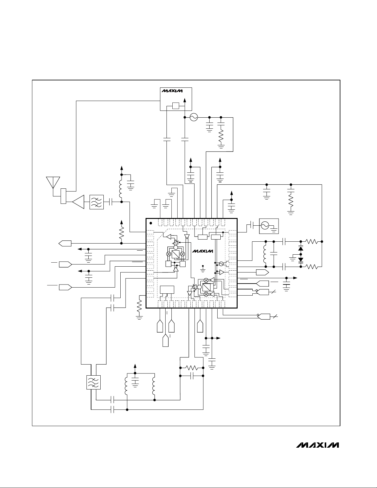
Detailed Description
The MAX2370 complete quadrature transmitter accepts
differential I/Q baseband inputs with external commonmode bias. A modulator upconverts the baseband
inputs to a 95MHz to 195MHz IF frequency. A gain-control voltage pin (GC) controls the gain of both the IF and
RF VGAs simultaneously to achieve the best current
consumption and linearity performance. The IF signal is
brought off-chip for filtering, then fed to a single sideband upconverter followed by the RF VGA and PA driver. The RF upconverter requires an external VCO for
operation. The IF PLL, RF PLL, and operating mode can
be programmed by an SPI/QSPI/ MICROWIRE-compatible 3-wire interface.
The following sections describe each block in the
Functional Diagram.
I/Q Modulator
Differential in-phase (I) and quadrature-phase (Q)
inputs are designed to be DC-coupled and biased with
the baseband output from a digital-to-analog converter
(DAC). The I and Q inputs need a typical DC bias of
VCC/ 2 and a current-drive capability of 8µA. However,
common-mode voltages in the 1.35V to (VCC- 1.25V)
range are also acceptable. The I and Q input capacitances are typically 0.6pF to ground on each pin. The
IF VCO output is fed into a divide-by-two quadrature
generator block to derive quadrature LO components
to drive the I/Q modulator. The output of the modulator
is fed into the IF VGA.
IF VCO
The IF VCO oscillates at twice the desired IF frequency.
The oscillation frequency is determined by external tank
components (see the IF Tank Design section). Typical
spurious performance for the IF VCO is shown in the
Typical Operating Characteristics.
IFLO Output Buffer
IFLO provides a buffered LO output when BUF_EN is 1.
The IFLO output frequency is equal to the IF VCO frequency, and the typical output power is -12dBm. This
output is intended for applications where the receive IF
is the same frequency as the transmit IF.
IF/RF PLL
The IF/RF PLL uses a charge-pump output to drive external loop filters. The loop filter is typically a passive second-order lead-lag filter. Outside the filter’s bandwidth,
phase noise is determined by the tank components. The
two components that contribute most significantly to
phase noise are the inductor and varactor. Use high-Q
inductors and varactors to maximize equivalent parallel
resistance. The IF_TURBO_CHARGE, RCP_TURBO1,
and RCP_TURBO2 bits can be set to enable turbo mode.
Turbo mode provides maximum charge-pump current
during frequency acquisition. Turbo mode is disabled
after frequency acquisition is achieved. When turbo
mode is disabled, charge-pump current returns to the
programmed levels as set by the ICP and RCP bits in the
CONFIG register (Table 3).
IF VGA
The IF VGA allows the IF output level to be controlled by
a voltage applied to the GC pin. The 0.5V to 2.5V voltage
range on GC provides a gain-control range of > 70dB,
with 2.5V providing maximum gain. The differential IF
output ports are optimized for the 95MHz to 195MHz frequency range. Do not allow VGCto exceed VCC- 0.2V
as this may cause oscillations at cold temperatures.
Single-Sideband Mixer and RF VGA
The RF transmit mixer uses a single-sideband architecture to eliminate an off-chip RF filter. The RF VGA follows the single-sideband mixer and is controlled by the
same GC voltage as the IF VGA to provide optimum
Complete 450MHz Quadrature Transmitter
8 _______________________________________________________________________________________
Pin Description (continued)
PIN NAME FUNCTION
40 RFCP
High-Impedance RF Charge-Pump Output. Connect to the tune input of the RF VCO through the
RF PLL loop filter. Keep the connection from RFCP to the tune input as short as possible to
prevent spurious pickup.
41 V
CCRFCP
Power Supply for the RF Charge Pump. This supply can be different from the system VCC. Bypass
to PC board ground with a minimum 0.1µF capacitor placed as close to the pin as possible. Do
not share capacitor ground vias with other ground connections.
42 RFPLL RF PLL Input. This port drives the RF PLL. RFPLL is internally biased to typically VCC - 0.8V.
44 LO RF LO Input. LO is internally biased to typically VCC - 0.8V.
45, 46, 48,
EP
GND
Ground Connection. Solder the exposed paddle (EP) evenly to the board’s ground plane for
proper operation.
Page 9

current consumption and linearity performance. The
power-control range of the RF VGA is typically 44dB.
PA Driver
The MAX2370 includes a PA driver that is optimized for
the 410MHz to 500MHz RF frequency range. The PA
driver is an open-collector output and requires a pullup
inductor to VCC. The pullup inductor can act as a shunt
element in a shunt-series matching network.
Programmable Registers
The MAX2370 includes eight programmable registers
consisting of four divide registers, a configuration register, an operational control register, a current control
register, and a test register. Each register consists of
24 bits. The 4 least significant bits (LSBs) are the register’s address. The 20 most significant bits (MSBs) are
used for register data. All registers contain some “don’t
care” bits. These can be either a 0 or 1 and do not
affect operation (Figure 1). Data is shifted in MSB first,
followed by the 4-bit address. When CS is low, the
clock is active and data is shifted with the rising edge
of the clock. When CS transitions to high, the shift register is latched into the register selected by the contents of the address bits. Typical register settings for
the eight registers are shown in Table 1. The dividers
and control registers are programmed from the
SPI/QSPI/MICROWIRE-compatible serial port.
The RFM register sets the main frequency divide ratio
for the RF PLL. The RFR register sets the reference frequency divide ratio. The RF VCO frequency can be
determined by the following:
RF VCO frequency = f
REF
x (RFM / RFR)
The IFM and IFR registers are similar:
IF VCO frequency = f
REF
x (IFM / IFR)
where f
REF
is the external reference frequency.
The operational control register (OPCTRL) controls the
state of the MAX2370. See Table 2 for a description of
each bit’s function.
The configuration register (CONFIG) sets the configuration for the RF and IF PLL and the baseband I/Q input
levels. See Table 3 for a description of each bit’s function.
The current-control register (I
CC
CTRL) modifies the bias
current to accommodate different operating modes. In
the high-power mode, MPL = 1 sets the bias current and
conversion gain to deliver an output power of at least
+5.5dBm from the PA drivers. In the low-noise mode,
MPL = 0 reduces output noise by 2.5dB for any given
output power at the expense of 3.4dB less maximum
obtainable output power.
Power Management
Bias control is distributed among several functional
sections and can be controlled to accommodate many
different power-down modes as shown in Table 8.
The serial interface remains active during shutdown.
Setting bit SHDN_BIT = 0 or pin SHDN = GND powers
down the device. In either case, PLL programming and
register information is retained.
Applications Information
3-Wire Serial Interface
Figure 3 shows the 3-wire interface timing diagram. The
3-wire bus is SPI/QSPI/MICROWIRE compatible.
Electromagnetic Compliance
Considerations
To produce a low-spur and EMC-compliant transmitter,
minimize circular current-loop area to reduce H-field
radiation. To minimize circular current-loop area, bypass
all VCCpins as close to the device as possible and use
the distributed capacitance of a ground plane. To minimize voltage drops, make VCCtraces short and wide.
Program only the necessary bits in any register to minimize cycling of the serial interface’s clock. RC filtering
can also be used to slow the clock edges on the 3-wire
interface, reducing high-frequency spectral content.
RC filtering also provides transient protection by shunting high frequencies to ground, while the series resistance attenuates the transients for error-free operation.
The same applies to the logic input pins (SHDN,
TXGATE, IDLE).
Place high-frequency bypass capacitors close to the
pins with a dedicated via for each capacitor to ground.
The 48-pin thin QFN-EP package provides minimal
ground inductance by using an exposed paddle under
the part. Provide at least five low-inductance vias under
the exposed paddle to ground. Use a solid ground
plane wherever possible. Any cutout in the ground
plane may act as a slot radiator and reduce its shield
effectiveness.
Keep RF LO traces as short as possible to reduce LO
radiation and susceptibility to interference.
IF Tank Design
The IF tank is fully differential. The external tank components for 120MHz IF operation are shown in the Typical
Application Circuit. See Maxim Application Note IF Tank
Design for the MAX2360 at www.maxim-ic.com for more
information on designing tanks for alternate IFs.
MAX2370
Complete 450MHz Quadrature Transmitter
_______________________________________________________________________________________ 9
Page 10

MAX2370
Internal to the IC, the charge pump has a leakage of less
than 10nA. This is equivalent to a 300MΩ shunt resistor.
The charge-pump output must see an extremely high
DC resistance of greater than 300MΩ. This minimizes
charge-pump spurs at the comparison frequency. Make
sure there is no solder flux under the varactor or loop filter
and use low-leakage capacitors.
Layout Considerations
The MAX2370 EV kit can be used as a starting point for
layout. For best performance, take into consideration
power-supply issues as well as RF, LO, and IF layout.
Power-Supply Layout
To minimize coupling between different sections of the
IC, the ideal power-supply layout is a star configuration,
which has a large decoupling capacitor at a central
VCCnode. The VCCtraces branch out from this node,
each going to a separate VCCpin of the MAX2370. At
the end of each trace is a bypass capacitor with impedance to ground less than 1Ω at the frequency of interest. This arrangement provides local decoupling at
each VCCpin. Use at least one via per bypass capacitor for a low-inductance ground connection. Also, connect the exposed paddle to the PC board GND with
multiple vias to provide the lowest inductance ground
connection possible.
Matching Network Layout
The layout of a matching network can be very sensitive to
parasitic circuit elements. To minimize parasitic inductance, keep all traces short and place components as
close to the IC as possible. To minimize parasitic capacitance, a cutout in the ground plane (and any other planes)
below the matching network components can be used.
Keep traces short on the high-impedance ports (e.g., IF
inputs and outputs) to minimize shunt capacitance.
Tank Layout
Keep the traces coming out of the tank short to reduce
series inductance and shunt capacitance. Keep the
inductor pads and coupling capacitor pads small to
minimize stray shunt capacitance.
Chip Information
PROCESS: BiCMOS
Complete 450MHz Quadrature Transmitter
10 ______________________________________________________________________________________
Page 11

MAX2370
Complete 450MHz Quadrature Transmitter
______________________________________________________________________________________ 11
MSB 24-BIT REGISTER LSB
DATA 20 BITS ADDRESS 4 BITS
B18 B16B19 B17 B14 B12B15 B13 B10 B8B11 B9 B6 B4B7 B5 B2 B0B3 B1 A2 A0A3 A1
RFM-DIVIDE RATIO (18) ADDRESS
X B16X B17 B14 B12B15 B13 B10 B8B11 B9 B6 B4B7 B5 B2 B0B3 B1 0 00 0
RFM-DIVIDE REGISTER
RFR-DIVIDE RATIO (13) ADDRESS
X XX X X B12X X B10 B8B11 B9 B6 B4B7 B5 B2 B0B3 B1 0 10 0
RFR-DIVIDE REGISTER
IFM-DIVIDE RATIO (14) ADDRESS
X XX X X B12X B13 B10 B8B11 B9 B6 B4B7 B5 B2 B0B3 B1 0 00 1
IFM-DIVIDE REGISTER
IFR-DIVIDE RATIO (11) ADDRESS
X XX X X XX X B10 B8X B9 B6 B4B7 B5 B2 B0B3 B1 0 10 1
IFR-DIVIDE REGISTER
OPERATION CONTROL BITS (16) ADDRESS
X XX X B14 B12B15 B13 B10 B8B11 B9 B6 B4B7 B5 B2 B0B3 B1 1 00 0
CONTROL REGISTER
CONFIGURATION BITS (16) ADDRESS
X XX X B14 B12B15 B13 B10 B8B11 B9 B6 B4B7 B5 B2 B0B3 B1 1 10 0
CONFIGURATION REGISTER
TEST REGISTER
CURRENT-CONTROL REGISTER
X = DON’T CARE
1
0 1
1B1B3B0B2B5B7B4B6
XX B8XXX XXXX XX
ADDRESS
1
0 0
1B1B3B0B2B5B7B4B6
B9B11 B8B10B13 B12B15XX XX
ADDRESSCURRENT CONTROL BITS (16)
B14
TEST BITS (9)
Figure 1. Register Configuration
Page 12

MAX2370
Complete 450MHz Quadrature Transmitter
12 ______________________________________________________________________________________
REGISTER NAME
TYPICAL
SETTINGS
REGISTER
ADDRESS
FUNCTION
RFM[17:0] 23000
DEC
0000
b
RF M-Divider Count
RFR[12:0] 384
DEC
0001
b
RF R-Divider Count
IFM[13:0] 4800
DEC
0010
b
IF M-Divider Count
IFR[10:0] 384
DEC
0011
b
IF R-Divider Count
OPCTRL[15:0] 090F
hex
0100
b
Operational Control Settings
CONFIG[15:0] D03F
hex
0101
b
Configuration and Setup Control
ICCCTRL[15:0] 0C38
hex
0110
b
Current Multiplication Factor, Throttle-Back Control, Modulator Bypass,
Compensation for Gain Variation Over Temperature, Maximum PowerLevel Setting
TEST[8:0] 100
hex
0111
b
Test Mode Control
Table 1. Register Settings for Typical Operation
Page 13

MAX2370
Complete 450MHz Quadrature Transmitter
______________________________________________________________________________________ 13
BIT NAME
BIT
(0 = LSB)
TYPICAL
SETTINGS
FUNCTION
RESERVED 15 0 Reserved. Set to 0 for normal operation.
RCP_TURBO1 14 0
Works with RCP_TURBO2 (in the configuration register) to set the turbo
charge-pump mode (see Table 7).
ICP_MAX 13 0
0 = N or m al op er ati on.
1 = S ets IF char g e- p um p cur r ent to tur b o l evel and keep s i t ther e even after
l ock i s estab l i shed . Thi s m od e p r ovi d es the hi g hest char g e- p um p cur r ent,
b ut effecti vel y no tur b o m od e si nce cur r ent i s al r ead y at m axi m um .
RESERVED 12, 11 01 Reserved. Set to 01 for normal operation.
RESERVED 10, 9 00 Reserved. Set to 00 for normal operation.
IFG 8, 7, 6 100
3-bit gain balancing control. Increases IF gain by approximately 2dB per
LSB. Provides a means for adjusting balance between RF and IF gain for
optimized linearity.
RESERVED 5 0 Reserved. Set to 0 for normal operation.
BUF_EN 4 0
LO buffer enable.
0 = LO buffer off.
1 = LO buffer on.
MOD_TYPE 3 1
Selects type of modulation.
0 = Selects direct VCO modulation (IF VCO is directly modulated and the
I/Q modulator is bypassed).
1 = Selects quadrature modulation.
STBY 21
Standby control.
0 = Shuts down everything except the registers and serial interface.
1 = Normal operation.
TXSTBY 11
Transmitter standby control.
0 = Shuts down the modulator and upconverter leaving PLLs locked and
registers active. This bit’s functionality is equivalent to that of the
TX_GATE pin.
1 = Normal operation.
SHDN_BIT 0 1
Shutdown control.
0 = Shuts down everything except the serial interface.
1 = Normal operation.
Table 2. Operation Control Register (OPCTRL, Address: 0100b)
LOCATION
Page 14

MAX2370
Complete 450MHz Quadrature Transmitter
14 ______________________________________________________________________________________
BIT NAME
BIT
(0 = LSB)
TYPICAL
SETTINGS
FUNCTION
RESERVED
0000 Reserved. Set to 0000 for normal operation.
MPL 11 1
Sets the maximum RF output power level.
0 = Sets to low-noise mode.
1 = Sets to normal power mode.
RESERVED 10, 9, 8, 7 1000 Reserved. Set to 1000 for normal operation.
THROTTLE_BACK
6, 5, 4 011 Controls the throttleback rate (see Table 6).
I_MULT 3, 2, 1, 0 1000 Sets the current scale factor for the PA driver (see Table 5).
Table 4. Current-Control Register (ICCCTRL, Address: 0110b)
BIT NAME
BIT
(0 = LSB)
TYPICAL
SETTINGS
FUNCTION
IF_PLL_SHDN 15 1
IF PLL shutdown control.
0 = Shuts down IF PLL. This mode is used with an external IF PLL.
1 = Normal operation.
RF_PLL_SHDN 14 1
RF PLL shutdown control.
0 = Shuts down RF PLL. This mode is used with an external RF PLL.
1 = Normal operation.
RESERVED 13 0 Reserved. Set to 0 for normal operation.
IQ_LEVEL 12 1
Selects the nominal I/Q input levels.
0 = Selects 300mV
P-P
input mode.
1 = Selects 600mV
P-P
input mode.
RESERVED 11, 10 00 Reserved. Set to 00 for normal operation.
ICP 9, 8 00
Sets the IF charge-pump current.
00 = 139µA.
01 = 192µA.
10 = 278µA.
11 = 390µA.
RCP 7, 6 00
Sets the RF charge-pump current.
00 = 325µA.
01 = 650µA.
10 = 738µA.
11 = 1063µA.
RESERVED 5, 4 11 Reserved. Set to 11 for normal operation.
IF_TURBO_CHARGE
31
IF tur b o- char g e contr ol .
0 = D i sab l es extr a char g e- p um p cur r ent d ur i ng acq ui si ti on.
1 = Acti vates tur b o- char g e featur e p r ovi d i ng extr a cur r ent d ur i ng acq ui si ti on.
RCP_TURBO2 2 1
Works with RCP_TURBO1 (in the operation control register) to set the
turbo charge-pump mode (see Table 7).
LD_MODE 1, 0 11
Determines output mode for LOCK pin as defined below:
00 = Test mode.
01 = IF PLL lock detector.
10 = RF PLL lock detector.
11 = Logical AND of IF PLL and RF PLL lock detectors.
Table 3. Configuration Register (CONFIG, Address: 0101b)
LOCATION
LOCATION
15, 14, 13, 12
Page 15

MAX2370
Complete 450MHz Quadrature Transmitter
______________________________________________________________________________________ 15
BIT NAME BITS
NOMINAL
CURRENT
SCALE FACTOR
0011 0.69
0100 0.75
0101 0.81
0110 0.88
0111 0.94
1000 (default) 1.00
1001 1.13
1010 1.25
1011 1.38
I_MULT
1100 1.50
Table 5. Typical Current Scale Factors
Set By I_MULT Bits
BIT NAME BITS
NOMINAL RATE
(dBmA/dB)
000 1.3
001 1.2
010 1.1
011 1.0
100 0.9
101 0.8
110 0.7
THROTTLE_BACK
111 0.6
Table 6. Typical Throttleback Rate Set By
THROTTLE_BACK Bits
RCP_TURBO1
FUNCTION
0 0 No turbo current. Charge-pump current is set by RCP bits.
01
Turbo current turns on every time RF PLL is reprogrammed. Turbo current is automatically
turned off after RF PLL is locked.
1 0 Turbo current is always on.
1 1 Turbo current is turned on every time RF PLL is out of lock.
Table 7. RF Turbo Charge-Pump Current Setting
POWER-DOWN MODE COMMENTS
UPCONVERTER
MODULATOR
RF PLL
IF VCO
IF PLL
SHDN Pin Ultra-low shutdown current OFF OFF OFF OFF OFF
IDLE Pin Rx only mode OFF OFF — OFF OFF
TXGATE Pin For punctured Tx mode OFF OFF ———
RF_PLL_SHDN Bit For external RF PLL use ——OFF ——
IF_PLL_SHDN Bit For external IF PLL use ————OFF
TXSTBY Bit Tx is OFF, but IF and RF LOs stay locked OFF OFF ———
Table 8. Power-Down Modes
RCP_TURBO2
Page 16
MAX2370
Complete 450MHz Quadrature Transmitter
16 ______________________________________________________________________________________
V
CC
0.1µF
0.1µF
400Ω
120MHz
BPF
V
CC
0.1µF
19.2MHz
TCXO
0.033µF
33pF
4.7pF
33pF
2pF TO
6.8pF
5.1kΩ
5.1kΩ
47nH
12kΩ
V
CC
100pF
47nH
DUPLEXER
PA
100pF
100pF
1000pF
0.022µF
20kΩ
V
CC
0.1µF
REF
N.C.
N.C.
N.C.
IFLO
V
CC
I+
I-
TANK+
TANK-
N.C.
LOCK
V
CCDRV
V
CC
IFIN+
IFIN-
RBIAS
N.C.
N.C.
N.C.
RFOUT
1
2
3
4
5
6
7
8
9
10
11
12
36
35
34
33
32
31
30
29
28
27
26
25
N.C.
IFOUT-
IFOUT+
V
CC
Q-
Q+
V
CC
N.C.
DI
CLK
N.C.
GND
GNDLON.C.
RFPLL
V
CCRFCP
RFCP
VCCV
CCIFCP
IFCP
GND
GC
4847464544434241403938
37
1314151617181920212223
24
CS
SHDN
IDLE
TXGATE
SHDN
IFLO
DAC
Q
DAC
I
RX
RECEIVER
RF
VCO
3300pF
0.047µF
/2
V
CC
100pF
V
CC
100pF
IDLE
TXGATE
LOCK
100pF
100pF
9.1pF
9.1pF
2.7pF
560Ω
10kΩ
100nH100nH
1000pF
V
CC
DI
CLK
CS
V
GC
51kΩ
V
CC
0.1µF
V
CC
0.1µF
V
CC
100pF
MAX2370
+45 -45
IF PLLRF PLL
Σ
Σ
SPI
INTERFACE
EP
90°
0°
/2
90°
0°
MAX2335
Figure 2. MAX2370 Typical Application Circuit
Page 17

MAX2370
Complete 450MHz Quadrature Transmitter
______________________________________________________________________________________ 17
t
CS
t
CH
t
CWL
t
CWH
DI
CLK
CS
t
ES
B19 (MSB) B18 B0 A3 A1 A0 (LSB)
tCS > 50ns
t
CH
> 10ns
t
CWH
> 50ns
t
ES
> 50ns
t
CWL
> 50ns
t
EW
> 50ns
t
EW
Figure 3. 3-Wire Interface Timing Diagram
Page 18

MAX2370
Complete 450MHz Quadrature Transmitter
18 ______________________________________________________________________________________
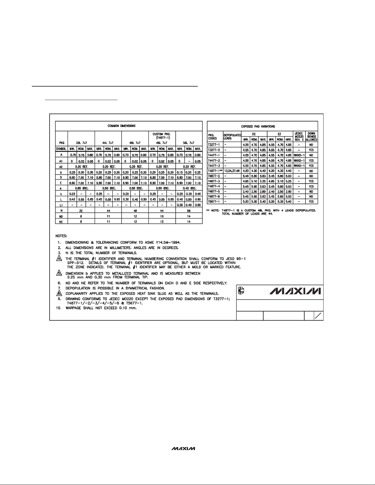
32, 44, 48L QFN.EPS
e
L
e
L
A1AA2
E/2
E
D/2
D
DETAIL A
D2/2
D2
b
L
k
E2/2
E2
(NE-1) X e
(ND-1) X e
e
C
L
C
L
C
L
C
L
k
DETAIL B
e
L
L1
PROPRIETARY INFORMATION
DOCUMENT CONTROL NO.APPROVAL
TITLE:
REV.
2
1
21-0144
DALLAS
SEMICONDUCTOR
PACKAGE OUTLINE
32, 44, 48, 56L THIN QFN, 7x7x0.8mm
D
Package Information
(The package drawing(s) in this data sheet may not reflect the most current specifications. For the latest package outline information
go to www.maxim-ic.com/packages
.)
Page 19
MAX2370
Complete 450MHz Quadrature Transmitter
Maxim cannot assume responsibility for use of any circuitry other than circuitry entirely embodied in a Maxim product. No circuit patent licenses are
implied. Maxim reserves the right to change the circuitry and specifications without notice at any time.
Maxim Integrated Products, 120 San Gabriel Drive, Sunnyvale, CA 94086 408-737-7600 ____________________ 19
© 2005 Maxim Integrated Products Printed USA is a registered trademark of Maxim Integrated Products, Inc.
PROPRIETARY INFORMATION
DOCUMENT CONTROL NO.APPROVAL
TITLE:
REV.
2
2
21-0144
DALLAS
SEMICONDUCTOR
PACKAGE OUTLINE
32, 44, 48, 56L THIN QFN, 7x7x0.8mm
D
Package Information (continued)
(The package drawing(s) in this data sheet may not reflect the most current specifications. For the latest package outline information
go to www.maxim-ic.com/packages
.)
 Loading...