

Page 1
General Description
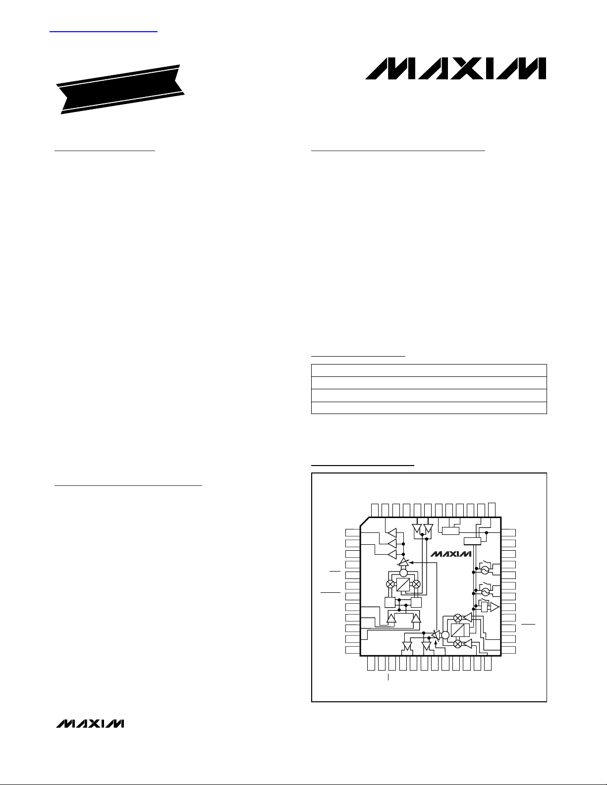
The MAX2360 dual-band, triple-mode complete transmitter for cellular phones represents the most integrated and
architecturally advanced solution to date for this application. The device takes a differential I/Q baseband input
and mixes it up to IF through a quadrature modulator and
IF variable-gain amplifier (VGA). The signal is then routed
to an external bandpass filter and upconverted to RF
through an SSB mixer and RF VGA. The signal is further
amplified with an on-board PA driver. Dual IF synthesizers, dual RF synthesizers, a local oscillator (LO) buffer,
and a 3-wire programmable bus complete the basic functional blocks of this IC. The MAX2362 supports singleband, single-mode (PCS) operation. The MAX2364
supports single-band cellular dual-mode operation.
The MAX2360 enables architectural flexibility because
its two IF voltage-controlled oscillators (VCOs), two IF
ports, two RF LO input ports, and three PA driver output
ports allow the use of a single receive IF frequency and
split-band PCS filters for optimum out-of-band noise
performance. The PA drivers allow up to three RF SAW
filters to be eliminated. Select a mode of operation by
loading data on the SPI™/QSPI™/MICROWIRE™-compatible 3-wire serial bus. Charge-pump current, sideband rejection, IF/RF gain balancing, standby, and
shutdown are also controlled with the serial interface.
The MAX2360/MAX2362/MAX2364 come in a 48-pin
TQFP-EP package and are specified for the extended
(-40°C to +85°C) temperature range.
Applications
Triple-Mode, Dual-Mode, or Single-Mode
Mobile Phones
Satellite Phones
Wireless Data Links (WAN/LAN)
Wireless Local Area Networks (LANs)
High-Speed Data Modems
High-Speed Digital Cordless Phones
Wireless Local Loop (WLL)
Features
♦ Dual-Band, Triple-Mode Operation
♦ +7dBm Output Power with -54dBc ACPR
♦ 100dB Power Control Range
♦ Supply Current Drops as Output Power Is Reduced
♦ Dual Synthesizer for IF and RF LO
♦ Dual On-Chip IF VCO
♦ QSPI/SPI/MICROWIRE-Compatible 3-Wire Bus
♦ Digitally Controlled Operational Modes
♦ +2.7V to +5.5V Operation
♦ Single Sideband Upconverter Eliminates SAW
Filters
MAX2360/MAX2362/MAX2364
Complete Dual-Band
Quadrature Transmitters
________________________________________________________________ Maxim Integrated Products 1
19-1635; Rev 1; 10/00
PART
MAX2360ECM
MAX2362ECM
MAX2364ECM
-40°C to +85°C
-40°C to +85°C
-40°C to +85°C
TEMP. RANGE PIN-PACKAGE
48 TQFP-EP*
48 TQFP-EP*
48 TQFP-EP*
SPI and QSPI are trademarks of Motorola, Inc.
MICROWIRE is a trademark of National Semiconductor Corp.
Pin Configurations appear at end of data sheet.
Selector Guide appears at end of data sheet.
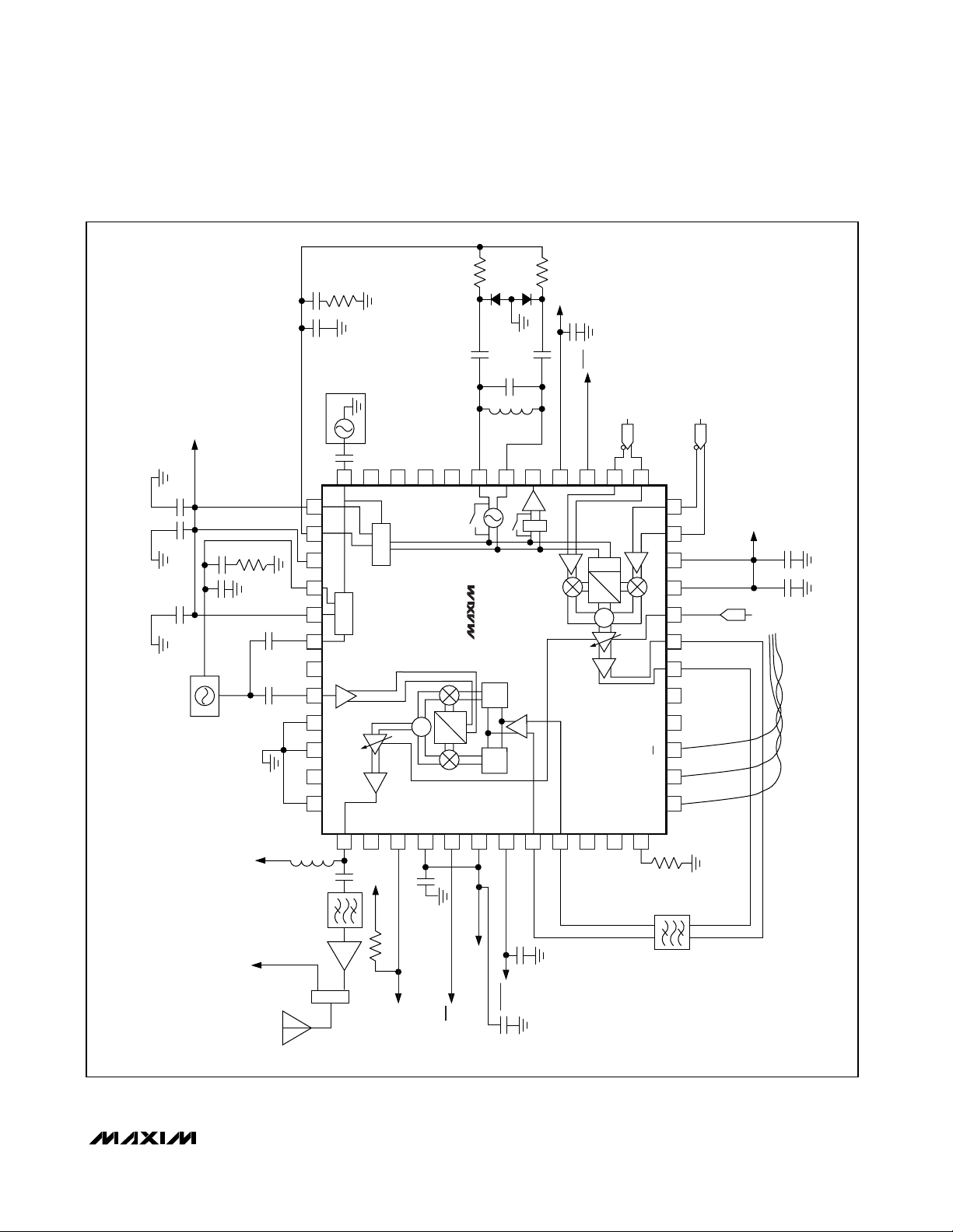
Functional Diagram
Ordering Information
*Exposed paddle
EVALUATION KIT
AVAILABLE
For pricing, delivery, and ordering information, please contact Maxim/Dallas Direct! at
1-888-629-4642, or visit Maxim’s website at www.maxim-ic.com.
查询MAX2360供应商
RFL
RFH0
LOCK
V
IDLE
V
TXGATE
IFINL+
IFINL-
IFINH+
IFINH-
R
BIAS
GND
RFH1
GND
GND
LOL
4847464544434241403938
1
2
3
4
CC
5
6
CC
7
8
9
10
11
12
Σ
90
0
+45 -45
1314151617181920212223
DI
CS
CLK
IFOUTH-
IFOUTH+
LOH
MAX2360
IFOUTL-
IFOUTL+
RFPLL
RFPLL
Σ
VGC
CC
V
0
RFCP
/2
90
CCVCC
V
VCCIFCP
IFPLL
CC
V
37
/2
24
Q-
Q+
36
REF
35
N.C.
34
N.C.
33
TANKH+
TANKH-
32
TANKL+
31
TANKL-
30
IFLO
29
V
28
CC
SHDN
27
I-
26
I+
25
Page 2
MAX2360/MAX2362/MAX2364
Complete Dual-Band
Quadrature Transmitters
2 _______________________________________________________________________________________
ABSOLUTE MAXIMUM RATINGS
ELECTRICAL CHARACTERISTICS
(MAX2360/2/4 test fixture: VCC= V
BATT
= 2.75V, SHDN = IDLE = TXGATE = 2.0V, VGC = 2.5V, R
BIAS
= 16kΩ, TA= -40°C to +85°C,
unless otherwise noted. Typical values are at T
A
= +25°C, and operating modes are defined in Table 6.)
Stresses beyond those listed under “Absolute Maximum Ratings” may cause permanent damage to the device. These are stress ratings only, and functional
operation of the device at these or any other conditions beyond those indicated in the operational sections of the specifications is not implied. Exposure to
absolute maximum rating conditions for extended periods may affect device reliability.
VCCto GND...........................................................-0.3V to +3.6V
RFL, RFH0, RFH1................................................................+5.5V
DI, CLK, CS, VGC, SHDN, TXGATE,
IDLE, LOCK................................................-0.3V to (V
CC
+ 0.3V)
AC Input Pins (IFINL, IFINH, Q, I, TANKL, TANKH,
REF, RFPLL, LOL, LOH)..........................................1.0V peak
Digital Input Current (SHDN, TXGATE, IDLE,
CLK, DI, CS) ................................................................±10mA
Continuous Power Dissipation (T
A
= +70°C)
48-Pin TQFP-EP (derate 27mW/°C above +70°C)...........2.16W
Operating Temperature Range ...........................-40°C to +85°C
Junction Temperature......................................................+150°C
Storage Temperature Range .............................-65°C to +160°C
Lead Temperature (soldering, 10s) .................................+300°C
50kΩ pull-up load (Note 6)
50kΩ pull-up load (Note 6)
SHDN = 0.6V (Note 6)
(Note 6)
(Note 6)
(Note 6)
(Note 6)
V0.4Lock Indicator Low
VV
CC
- 0.4Lock Indicator High
kΩ225 280VGC Input Resistance During Shutdown
µA-10 +10VGC Input Current
µA-5 +5Logic Input Current
V0.6Logic Low
V2.0Logic High
µA0.5 20
26 34
15 20
97 123
92 118
V2.7 3.0Operating Supply Voltage
6.5 9.5
114 142
89 114
85 110
Operating Supply Current
132 161
91 110
95 122
mA
132 164
UNITS
MIN TYP MAX
PARAMETER
PCS mode
SHDN = 0.6V, sleep mode
Addition for IFLO buffer
FM mode
Cellular
digital mode
VGC = 2.0V
VGC = 0.5V
VGC = 2.5V
STBY = 0.6V,
TXGATE = 0.6V
VGC = 2.0V
VGC = 0.5V
VGC = 2.5V
VGC = 0.5V
VGC = 2.0V
IDLE = 0.6V, cell idle
VGC = 2.5V
CONDITIONS
(Note 1)
11RFPLL off
Page 3

MAX2360/MAX2362/MAX2364
Complete Dual-Band
Quadrature Transmitters
_______________________________________________________________________________________ 3
ELECTRICAL CHARACTERISTICS
(MAX2360/62/64 evaluation kit, 50Ω system, operating modes as defined in Table 6, input voltage at I and Q = 200mV
RMS
differen-
tial, common mode = V
CC
/2, 300kHz quadrature CW tones, RF and IF synthesizers locked with passive lead-lag second-order loop
filter, REF = 200mVp-p at 19.68MHz, V
CC
= SHDN = IDLE = CS = TXGATE = 2.75V, V
BAT
= 2.75V, IF output load = 400Ω, LOH, LOL
input power = -7dBm, f
LOL
= 966MHz, f
LOH
= 1750MHz, IFINH = 125mV
RMS
at 130MHz, IS-95 CDMA modulation f
RFH0
= f
RFH1
=
1880MHz, f
RFL
= 836MHz, TA= +25°C, unless otherwise noted.)
Gain Variation Over Temperature -1 +1 dB
Relative to +25°C, TA= -40°C to +85°C
(Note 4)
Gain Variation Over Temperature ±1 ±2 dB
LO Leakage -17 dBm
Image Signal -29 dBc
Relative to +25°C, TA= -40°C to +85°C
(Note 4)
PARAMETER
MIN TYP MAX
UNITS
Carrier Suppression 30 49 dB
IF Output Power at IFOUTL and IFOUTH,
CDMA Mode
-10 dBm
IF Gain Control Range 85 dB
I/Q Common-Mode Input Voltage
1.35 VCC/2
V
CC
-
1.25
V
Sideband Suppression 30 38 dB
IF Gain Control Range 85 dB
Output Power at IFOUTL -8.5 dBm
120–235
IF Frequency Range
120–300
MHz
Output Power at IFOUTL -5.5 dBm
120–200
IF Frequency Range
180–300
MHz
RFL Frequency Range 800–1000 MHz
RFH Frequency Range 1700–2000 MHz
LOL Frequency Range 800–1150 MHz
LOH Frequency Range 1400–2300 MHz
RFPLL Frequency Range
Output Power, RFL Port
7
dBm
Output Power, RFH1 Port 7.5 dBm
Output Power, RFH0 Port 6.6 dBm
Power Control Range 30 dB
CONDITIONS
VGC = 2.5V, IFG = 111,
direct VCO modulation
VGC = 2.5V, IFG = 100
VGC = 2.5V, IFG = 100, ACPR = -70dBc
VGC = 0.5V to 2.5V, IFG = 100
VCC= 2.7V to 3.0V (Notes 2, 3, 6)
VGC = 2.5V, IFG = 100
IF_BAND = low
IF_BAND = high
VGC = 0.5V to 2.5V, IFG = 100
VGC = 2.5V, IFG = 111, I/Q modulation
RFL port
RFH0 and RFH1 ports
IF_BAND = low
VGC = 2.5V
IF_BAND = high
VGC = 2.6V, ACPR = -54dBc
VGC = 2.6V, ACPR = -54dBc
VGC = 0.5V to 2.5V
ACPR = -54dBc
FM mode 12
MHz
1300Cellular frequency operation
2300PCS frequency operation
MODULATOR, QUADRATURE MODES (CDMA, PCS, FM_IQ)
MODULATOR, FM MODE
UPCONVERTER AND PREDRIVER
Page 4
MAX2360/MAX2362/MAX2364
Complete Dual-Band
Quadrature Transmitters
4 _______________________________________________________________________________________
ELECTRICAL CHARACTERISTICS (continued)
(MAX2360/62/64 evaluation kit, 50Ω system, operating modes as defined in Table 6, input voltage at I and Q = 200mV
RMS
differen-
tial, common mode = V
CC
/2, 300kHz quadrature CW tones, RF and IF synthesizers locked with passive lead-lag second-order loop
filter, REF = 200mVp-p at 19.68MHz, V
CC
= SHDN = IDLE = CS = TXGATE = 2.75V, V
BAT
= 2.75V, IF output load = 400Ω, LOH, LOL
input power = -7dBm, f
LOL
= 966MHz, f
LOH
= 1750MHz, IFINH = 125mV
RMS
at 130MHz, IS-95 CDMA modulation f
RFH0
= f
RFH1
=
1880MHz, f
RFL
= 836MHz, TA= +25°C, unless otherwise noted.)
Note 1: See Table 6 for register settings.
Note 2: ACPR is met over the specified V
CM
range.
Note 3: V
CM
must be supplied by the I/Q baseband source with ±6µA capability.
Note 4: Guaranteed by design and characterization.
Note 5: When enabled, turbolock is active during acquisition and injects boost current in addition to the normal charge-pump current.
Note 6: >25°C guaranteed by production test, <25°C guaranteed by design and characterization.
RFPLL Input Sensitivity 160 mVp-p
Charge-Pump High-Z Leakage 10 nAOver specified compliance range
Charge-Pump Source/Sink Matching 5 %
Locked, all values of RCP, over specified
compliance range (Note 6)
ICP = 00 (Note 6)
PARAMETER
MIN TYP MAX
UNITS
VCO Operating Range
240–600
MHz
240–470
IF Reference Divider Ratio 2 2048
IF Main Divide Ratio 256 16384
IF LO Output Power -6 dBm
115 175 230
145 235 315
235 350 470
Reference Frequency 530MHz
Frequency Reference Signal Level 0.1 0.6 Vp-p
Charge-Pump Source/Sink Current
300 465 625
µA
Turbolock Boost Current 265 450 615 µA
Charge-Pump Source/Sink Matching 5 %
Charge-Pump High-Z Leakage 10 nA
RF Main Divide Ratio 4096 262144
RF Reference Divide Ratio 2 8192
Maximum Phase-Detector Comparison
Frequency
10 MHz
100 165 225
µA
Charge-Pump Source/Sink Current
100 165 225
µA
CONDITIONS
VCO = low
(Notes 5, 6)
BUF_EN = 1
Locked, all values of ICP, over specified
compliance range (Note 6)
Over specified compliance range
RCP = 00 (Note 6)
135 230 310RCP = 01 (Note 6)
270 450 630RCP = 11 (Note 6)
210 340 460RCP = 10 (Note 6)
Turbolock Boost Current 245 435 630 µA(Notes 5, 6)
IF_PLL
RF_PLL
ICP = 11 (Note 6)
ICP = 10 (Note 6)
ICP = 01 (Note 6)
VCO = high
Page 5
MAX2360/MAX2362/MAX2364
Complete Dual-Band
Quadrature Transmitters
_______________________________________________________________________________________ 5
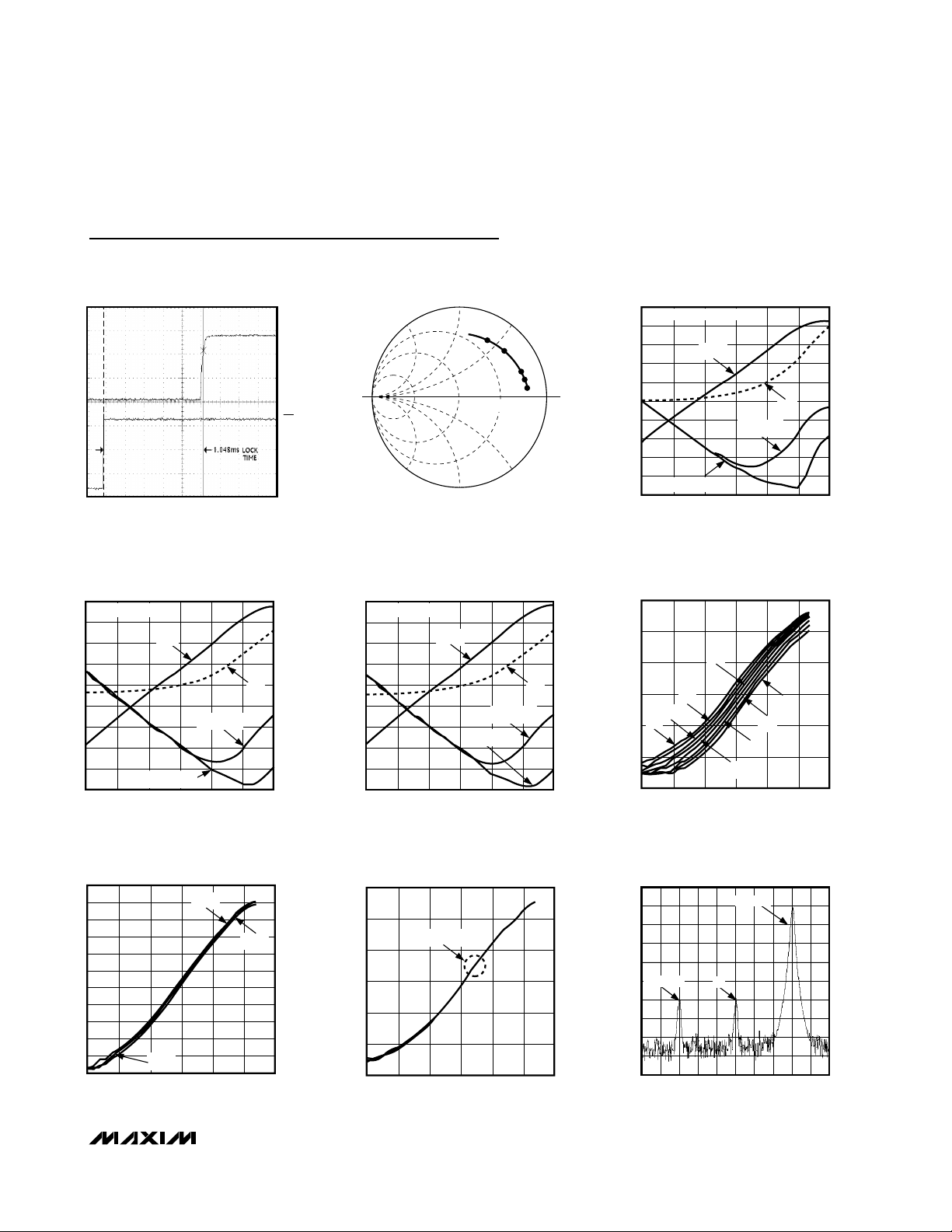
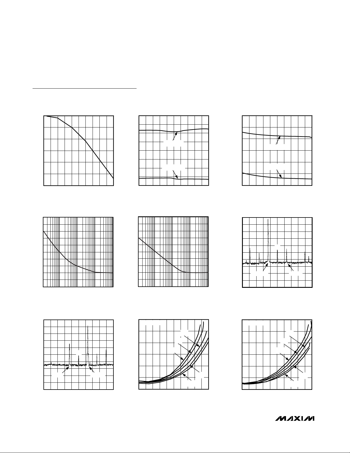
Typical Operating Characteristics
(MAX2360EVKIT, VCC= +2.75V, TA= +25°C, unless otherwise noted.)
TIME (200µs/div)
IF VCO VOLTAGE vs. TIME
MAX2360/2/4-01
LOCK
VOLTS (1V/div)
CS
TANK 1/S11 vs. FREQUENCY
MAX2360/2/4-02
4
5
1
2
3
z0 = 200Ω
EQUIVALENT PARALLEL R-C
1: 200MHz, 1.76kΩ, 0.26pF
2: 260MHz, 1.66kΩ, 0.31pF
3: 330MHz, 1.58kΩ, 0.34pF
4: 780MHz, 1.21kΩ, 0.43pF
5: 1GHz, 0.94kΩ, 0.47pF
-80
-50
-60
-70
-10
-20
-30
-40
0
10
20
56
38
20
128
110
92
74
146
182
200
1.5 1.9 2.11.7 2.3 2.5 2.7
OUTPUT POWER, ACPR, ICC vs. VGC
MAX2360/2/4-03
VGC (V)
P
OUT
(dBm), ACPR/ALTR (dBc)
I
CC
(mA)
I
CC
P
OUT
ALTERNATE
ADJACENT
CELLULAR CDMA, RFL
164
-80
-60
-70
-20
-30
-40
-50
-10
0
10
60
40
20
140
120
100
80
160
180
200
1.5 1.9 2.11.7 2.3 2.5 2.7
OUTPUT POWER, ACPR,
I
CC
vs. VGC
MAX2360/2/4-04
VGC (V)
P
OUT
(dBm), ACPR/ALTR (dBc)
I
CC
TOTAL (mA)
I
CC
ADJACENT
ALTERNATE
P
OUT
PCS CDMA, RFH0
-80
-50
-60
-70
-20
-30
-40
-10
0
10
1.5 1.9 2.11.7 2.3 2.5 2.7
OUTPUT POWER, ACPR,
I
CC
TOTAL vs. VGC
MAX2360/2/4-05
VGC (V)
P
OUT
(dBm), ACPR/ALTR (dBc)
20
80
60
40
140
120
100
160
180
200
I
CC
TOTAL (mA)
P
OUT
I
CC
ADJACENT
ALTERNATE
PCS CDMA, RFH1
-120
-80
-100
-40
-60
-20
0
0 1.0 1.50.5 2.0 2.5 3.0
IF OUTPUT POWER
vs. VGC AND IF DAC SETTING
MAX2360/2/4-06
VGC (V)
P
OUT
(dBm)
011
111
100
101
110
001
000
010
-110
-90
-100
-40
-50
-60
-70
-80
-30
-20
-10
0
1.00 1.50.5 2.0 2.5 3.0
IF OUTPUT POWER vs. VGC
MAX2360/2/4-07
VGC (V)
IF POWER
(dBm)
-40°C
+85°C
+25°C
-120
-80
-100
-40
-60
-20
0
0 1.0 1.50.5 2.0 2.5 3.0
IF OUTPUT POWER vs. VGC
MAX2360/2/4-08
VGC (V)
P
OUT
(dBm)
2.7V, 3.0V, 3.3V
-100
-30
-40
-20
-10
0
-80
-90
-70
-60
-50
130.18129.98 130.38 130.58 130.78
SIDEBAND SUPPRESSION AND
LO FEEDTHROUGH (IFOUTH)
MAX2360/2/4-09
FREQUENCY (MHz)
P
OUT
(dBm)
DESIRED
LO
SIDEBAND
Page 6
MAX2360/MAX2362/MAX2364
Complete Dual-Band
Quadrature Transmitters
6 _______________________________________________________________________________________
Typical Operating Characteristics (continued)
(MAX2360EVKIT, VCC= +2.75V, TA= +25°C, unless otherwise noted.)
IFOUTH DIFFERENTIAL PORT
I/Q BASEBAND FREQUENCY RESPONSE
0
-0.5
-1.0
-1.5
(dBc)
-2.0
-2.5
-3.0
020155 10 253035404550
FREQUENCY (MHz)
MAX2360/2/4-10
800
700
600
500
400
300
200
PARALLEL RESISTANCE (Ω)
100
0
OUTPUT IMPEDANCE
RESISTANCE
CAPACITANCE
180160120 140100 200 220 240 260 280 300
FREQUENCY (MHz)
MAX2360/2/4-11
4.0
3.5
3.0
2.5
2.0
1.5
1.0
0.5
0
600
500
400
300
200
PARALLEL RESISTANCE (Ω)
PARALLEL CAPACITANCE (pF)
100
0
IFINH DIFFERENTIAL PORT
INPUT IMPEDANCE
RESISTANCE
CAPACITANCE
180160120 140100 200 220 240 260 280 300
FREQUENCY (MHz)
MAX2360/2/4-12
6
5
4
3
2
PARALLEL CAPACITANCE (pF)
1
0
PHASE NOISE LOW-BAND OSCILLATOR
vs. FREQUENCY OFFSET (130.38MHz)
-50
-60
-70
-80
-90
-100
(dBc/Hz)
-110
-120
-130
-140
-150
1k 10M
10k
FREQUENCY (Hz)
100k
1M
MAX2360/2/4-13
PHASE NOISE HIGH-BAND OSCILLATOR
vs. FREQUENCY OFFSET (165MHz)
-50
-60
-70
-80
-90
-100
(dBc/Hz)
-110
-120
-130
-140
-150
10k 100k
1k 10M
FREQUENCY (Hz)
1M
RFHO CASCADE ACPR
AND V
10
0
-10
-20
-30
-40
-50
AMPLITUDE (dBm)
-60
-70
-80
-90
IMAGE
RFH0 OUTPUT SPECTRUM
LO
DESIRED
15501350 1750 1950 2150
FREQUENCY (MHz)
MAX2360/2/4-16
-40
-45
-50
-55
ACPR (dBc)
-60
-65
-70
VCC = 2.75V
vs. P
OUT
-2-4-8 -6-10 0246810
P
OUT
BAT
3.0V
2.8V
2.7V
3.6V
(dBm)
3.3V
MAX2360/2/4-14
MAX2360/2/4-17
10
0
-10
-20
-30
-40
-50
AMPLITUDE (dBm)
-60
-70
-80
-90
CASCADE ACPR vs. P
-40
VCC =
-45
-50
-55
ACPR (dBc)
-60
-65
-70
RFL OUTPUT SPECTRUM
LO
2.7V
(dBm)
2.8V
OUT
IMAGE
AND V
3.0V
3.6V
DESIRED
766.38566.38 966.38 1166.38 1366.38
FREQUENCY (MHz)
2.75V
-2-4-8 -6-10 0246810
P
OUT
MAX2360/2/4-15
BAT
MAX2360/2/4-18
3.3V
Page 7
Complete Dual-Band
Quadrature Transmitters
_______________________________________________________________________________________ 7
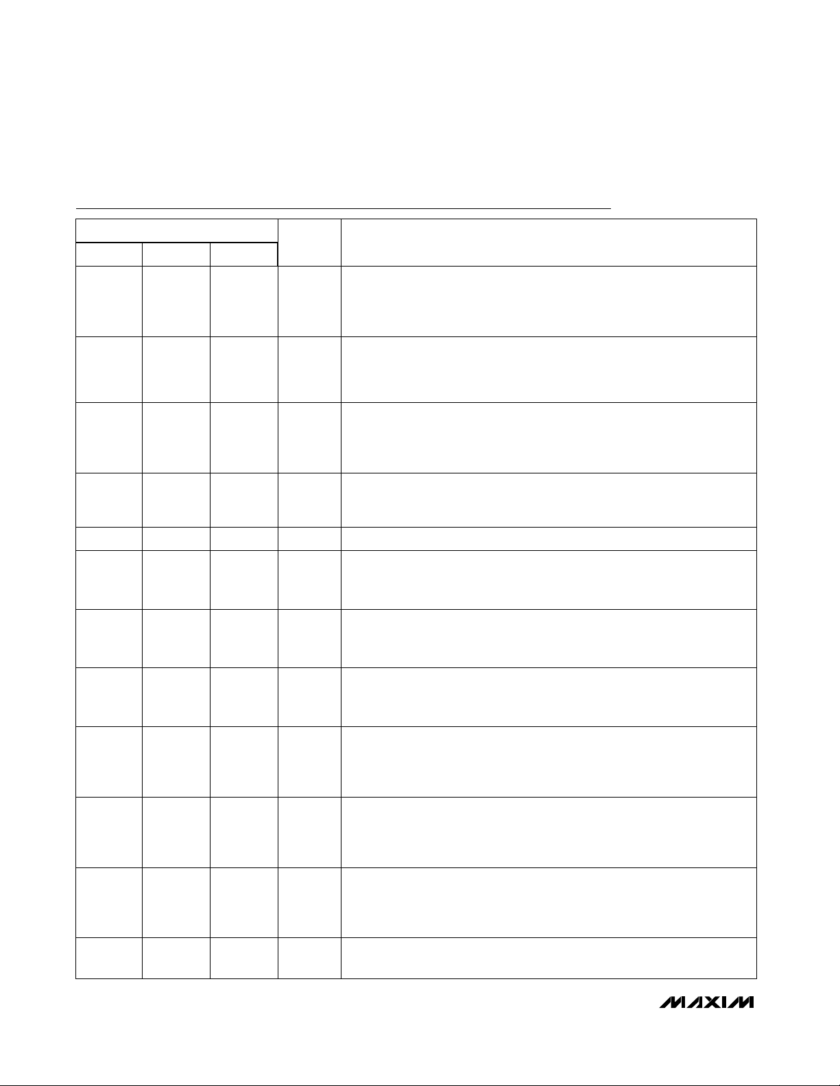
Typical Operating Characteristics (continued)
(MAX2360EVKIT, VCC= +2.75V, TA= +25°C, unless otherwise noted.)
MAX2360/MAX2362/MAX2364
-100
-80
-90
-60
-70
-40
-50
-30
-10
-20
0
129.78129.18 130.38 130.98 131.58
BUFFERED LO OUTPUT
MAX2360/2/4-22
FREQUENCY (MHz)
AMPLITUDE (dBm)
LOL PORT S11
MAX2360/2/4-23
1: 700MHz, 72Ω –j51Ω
2: 966MHz, 60Ω –j46Ω
3: 1.22MHz, 52Ω –j38Ω
4: 1.5GHz, 40Ω –j25Ω
4
1
2
3
LOH PORT S11
MAX2360/2/4-24
1600MHz TO 2500MHz
1: 1.6GHz, 40Ω –j25Ω
2: 1.75GHz, 36Ω –j22Ω
3: 1.88GHz, 34Ω –j18Ω
4: 2.01GHz, 32Ω –j15Ω
5: 2.5GHz, 29Ω –j0Ω
4
5
1
2
3
ICC vs. RFL OUTPUT POWER (836MHz)
180
170
160
150
(mA)
140
CC
I
130
120
110
100
-60 -40-50 -30 -20 -10 0 10
OUTPUT POWER (dBm)
MAX2360/2/4-19
ICC vs. RFH0 OUTPUT POWER (1880MHz)
180
170
160
150
(mA)
140
CC
I
130
120
110
100
-60 -40-50 -30 -20 -10 0 10
OUTPUT POWER (dBm)
MAX2360/2/4-21
ICC vs. RFH1 OUTPUT POWER (1880MHz)
180
170
160
150
(mA)
140
CC
I
130
120
110
100
-60 -40-50 -30 -20 -10 0 10
OUTPUT POWER (dBm)
MAX2360/2/4-21
Page 8
MAX2360/MAX2362/MAX2364
Complete Dual-Band
Quadrature Transmitters
8 _______________________________________________________________________________________
Pin Description
MAX2360
PIN
NAME FUNCTION
MAX2364MAX2362
1 — 1 RFL
Transmitter RF Output for Cellular Band (800MHz to 1000MHz)—for both FM
and digital modes. This open-collector output requires a pull-up inductor to
the supply voltage, which may be part of the output matching network and
may be connected directly to the battery.
No Connection. Make no connection to these pins.N.C.
2, 10, 11,
16, 17,
32–35
43, 47
1, 8, 9, 18,
19, 30, 31,
34, 35, 44
—
2 2 — RFH0
Transmitter RF Output for PCS Band (1700MHz to 2000MHz). This opencollector output requires a shunt inductor to the supply voltage. The pull-up
inductor may be part of the output matching network and may be connected
directly to the battery.
Open-Collector Output Indicating Lock Status of the IF and/or the RF PLLs.
Requires a pull-up resistor. Control using configuration register bit LD_MODEO,
LD_MODE1.
LOCK333
4 4 4 V
CC
Power Supply
Digital Input. A logic low on IDLE shuts down everything except the RF PLL
and associated registers. A small RC lowpass filter may be used to prevent
digital noise.
IDLE
555
6 6 6 V
CC
Supply Pin for the Upconverter Stage. VCCmust be bypassed to system
ground as close to the pin as possible. The ground vias for the bypass
capacitor should not be shared by any other branch.
Digital Input. A logic low on TXGATE shuts down everything except the RF
PLL, IF PLL, IF VCO, and serial bus and registers. This mode is used for
gated transmission.
TXGATE
777
8, 9 — 8, 9
IFINL+,
IFINL-
Differential Inputs to the RF Upconverter. These pins are internally biased to
1.5V. The input impedance for these ports is nominally 400Ω differential. The
IF filter should be AC-coupled to these ports. Keep the differential lines as
short as possible to minimize stray pick-up and shunt capacitance.
IFINH+,
IFINH-
—10, 1110, 11
12 12 12 R
BIAS
Bias Resistor Pin. RBIAS is internally biased to a bandgap voltage of 1.18V. An
external resistor or current source must be connected to this pin to set the bias
current for the upconverters and PA driver stages. The nominal resistor value is
16kΩ. This value can be altered to optimize the linearity of the driver stage.
Input Pins from the 3-Wire Serial Bus (SPI/QSPI/MICROWIRE compatible).
An RC filter on each of these pins may be used to reduce noise.
CLK, DI,
CS
13, 14, 1513, 14, 1513, 14, 15
Page 9

MAX2360/MAX2362/MAX2364
Complete Dual-Band
Quadrature Transmitters
_______________________________________________________________________________________ 9
Pin Description (continued)
I+, I-
SHDN
V
CC
IFLO
TANKL-,
TANKL+
VGC
V
CC
V
CC
Q+, Q-
IFOUTL+,
IFOUTL-
IFOUTH-,
IFOUTH+
NAME
25, 26
27
28
29
30, 31
20
21
22
23, 24
18, 19
—
MAX2364
PIN
Differential I-Channel Baseband Inputs to the Modulator. These pins go
directly to the bases of a differential pair and require an external commonmode bias voltage of 1.4V.
25, 2625, 26
Shutdown Input. A logic low on SHDN shuts down the entire IC. An RC lowpass filter may be used to reduce digital noise.
2727
Supply Pin to the VCO Section. Bypass as close to the pin as possible. The
bypass capacitor should not share its vias with any other branches.
2828
Buffered LO Output. Control the output buffer using register bit BUF_EV and
the divide ratio using the register bit BUF_DIV.
2929
Differential Tank Pins for the Low-Frequency IF VCO. These pins are internally
biased to 1.6V.
—30, 31
RF and IF Variable-Gain Control Analog Input. VGC floats to 1.5V. Apply
0.5V to 2.6V to control the gain of the RF and IF stages. An RC filter on this
pin may be used to reduce DAC noise or PDM clock spurs from this line.
2020
Supply Pin for the IF VGA. Bypass with a capacitor as close to the pin as
possible. The bypass capacitor must not share its ground vias with any other
branches.
2121
Supply for the I/Q Modulator. Bypass with capacitor as close to the pin as
possible. The bypass capacitor must not share its ground vias with any other
branches.
2222
Differential Q-Channel Baseband Inputs to the Modulator. These pins go
directly to the bases of a differential pair and require an external commonmode bias voltage.
23, 2423, 24
Differential IF Outputs. These ports are active when the register bit IF_SEL is
low. These pins must be inductively pulled up to V
CC
. A differential IF bandpass filter is connected between this port and IFINL+ and IFINL-. The pull-up
inductors can be part of the filter structure. The differential output impedance
of this port is nominally 600Ω. The transmission lines from these pins should
be short to minimize the pick-up of spurious signals and noise.
—18, 19
Differential IF Outputs. These ports are active when the register bit IF_SEL is
high. They do not support FM mode. These pins must be inductively pulled
up to V
CC
. A differential IF bandpass filter is connected between this port
and IFINH+ or IFINH-. The pull-up inductors can be part of the filter structure.
The differential output impedance of this port is nominally 600Ω. The transmission lines from these pins should be short to minimize the pick-up of spurious signals and noise.
16, 1716, 17
FUNCTION
MAX2362
MAX2360
Page 10

MAX2360/MAX2362/MAX2364
Complete Dual-Band
Quadrature Transmitters
10 ______________________________________________________________________________________
Pin Description (continued)
GND
Exposed
paddle
DC and AC GND Return for the IC. Connect to PC board ground plane using
multiple vias.
Exposed
paddle
Exposed
paddle
RFH1—
Transmitter RF Output for PCS Band (1700MHz to 2000MHz). This open-collector output requires a shunt inductor to the supply voltage. The pull-up
inductor may be part of the output matching network and may be connected
directly to the battery.
4747
GND45, 46, 48 Ground. Connect to PCB ground plane.45, 46, 4845, 46, 48
RFCP
V
CC
RFPLL
LOH
LOL
REF
V
CC
IFCP
V
CC
N.C.
TANKH-,
TANKH+
NAME
40
41
42
—
44
36
37
38
39
34, 35
—
MAX2364
PIN
High-Impedance Output of the RF Charge Pump. Connect to the tune input of
the RF VCOs through the RF PLL loop filter. Keep the line from this pin to the
tune input as short as possible to prevent spurious pick-up, and connect the
loop filter as close to the tune input as possible.
4040
Supply for the RF Charge Pump. This supply can differ from the system VCC.
Bypass as close to the pin as possible. The bypass capacitor must not share
its vias with any other branches.
4141
RF PLL Input. AC-couple this port to the RF VCO.4242
High-band RF LO Input Port. AC-couple to this port.4343
Low-band RF LO Input Port. AC-couple to this port.—44
Reference Frequency Input. REF is internally biased to VCC- 0.7V and must
be AC-coupled to the reference source. This is a high-impedance port
(25kΩ
II
3pF).
3636
Supply for the IF Charge Pump. This supply can differ from the system VCC.
Bypass as close to the pin as possible. The bypass capacitor must not share
its vias with any other branches.
3737
High-Impedance Output of the IF Charge Pump. Connect to the tune input of
the IF VCOs through the IF PLL loop filter. Keep the line from IFCP to the tune
input as short as possible to prevent spurious pick-up, and connect the loop
filter as close to the tune input as possible.
3838
Supply Pin for Digital Circuitry. Bypass as close to the pin as possible. The
bypass capacitor must not share its vias with any other branch.
3939
No Connection. Leave these pins floating.34, 3534, 35
Differential Tank Pins for the High-Frequency IF VCO. These pins are internally
biased to 1.6V.
32, 3332, 33
FUNCTION
MAX2362
MAX2360
Page 11

MAX2360/MAX2362/MAX2364
Complete Dual-Band
Quadrature Transmitters
______________________________________________________________________________________ 11
Detailed Description
The MAX2360 complete quadrature transmitter accepts
differential I/Q baseband inputs with external commonmode bias. A modulator upconverts this to IF frequency
in the 120MHz to 300MHz range. A gain control voltage
pin (VGC) controls the gain of both the IF and RF VGAs
simultaneously to achieve best noise and linearity performance. The IF signal is brought off-chip for filtering,
then fed to a single sideband upconverter followed by
the RF VGA and PA driver. The RF upconverter requires
an external VCO for operation. The IF PLL, RF PLL, and
operating mode can be programmed by an SPI/QSPI/
MICROWIRE-compatible 3-wire interface.
The following sections describe each block in the
MAX2360 Functional Diagram.
I/Q Modulator
Differential in-phase (I) and quadrature-phase (Q) input
pins are designed to be DC-coupled and biased with the
baseband output from a digital-to-analog converter
(DAC). I and Q inputs need a DC bias of VCC/2 and a
current-drive capability of 6µA. Common-mode voltage
will work within a +1.35V to (VCC- 1.25V) range.
Typically, I and Q will be driven differentially with a
200mV
RMS
baseband signal. Optionally, I and Q may be
programmed for 100mV
RMS
operation with the IQ_LEVEL
bit in the configuration register. The IF VCO output is fed
into a divide-by-two/quadrature generator block to derive
quadrature components to drive the IQ modulator. The
output of the modulator is fed into the VGA.
IF VCOs
There are two VCOs to support high IF and low IF applications. The VCOs oscillate at twice the desired IF frequency. Oscillation frequency is determined by external
tank components (see Applications Information).
Typical phase-noise performance for the tank is as
shown in Table 1. The high-band and low-band VCOs
can be selected independently of the IF port being
used.
IFLO Output Buffer
IFLO provides a buffered LO output when BUF_EN is 1.
The IFLO output frequency is equal to the VCO frequency when BUF_DIV is 0, and half the VCO frequency when BUF_DIV is 1. The output power is -6dBm. This
output is intended for applications where the receive IF
is the same frequency as the transmit IF.
IF/RF PLL
The IF/RF PLL uses a charge-pump output to drive a
loop filter. The loop filter will typically be a passive second-order lead lag filter. Outside the filter’s bandwidth,
phase noise will be determined by the tank components. The two components that contribute most significantly to phase noise are the inductor and varactor.
Use high-Q inductors and varactors to maximize equivalent parallel resistance. The IF_TURBO_CHARGE and
the RF_TURBO_CHARGE bits in the CONFIG register
can be set to 1 to enable turbo mode. Turbo mode provides maximum charge-pump current during frequency
acquisition. Turbo mode is disabled after the second
transition from phase lead to phase lag or from phase
lag to phase lead. Turbo mode is also disabled after
frequency acquisition is achieved. When turbo mode is
disabled, charge-pump current will return to the programmed levels as set by ICP and RCP bits in the
CONFIG register (Table 4).
IF VGA
The IF VGA allows varying an IF output level that is controlled by the VGC. The voltage range on VGC of 0.5V
to 2.6V. provide a gain-control range of 85dB. There
are two differential IF output ports from the VGA.
IFOUTL+/IFOUTL- are optimized for low IF operation
(120MHz to 235MHz) for IFOUTH+/IFOUTH- support
high IF operation (120MHz to 300MHz). IFOUTL ports
support direct VCO FM modulation. The differential IF
output port has an output impedance of 600Ω when
pulled up to VCCthrough a choke.
Single Sideband Mixer
The RF transmit mixer uses a single sideband architecture to eliminate an off-chip RF filter. The single sideband
mixer has IF input stages that correspond to IF output
ports of the VGA. The mixer is followed by the RF VGA.
The RF VGA is controlled by the same VGC pin as the IF
VGA to provide optimum linearity and noise performance. The total power control range is >100dB.
PA Driver
The MAX2360 includes three power-amplifier (PA) drivers. Each is optimized for the desired operating frequency. RFL is optimized for cellular-band operation.
Table 1. Typical VCO Phase Noise
(IF = 130.38MHz)
30
12.5
1
OFFSET (kHz) PHASE NOISE (dBc)
-80
-105
-111
900
120 -121
-128
Page 12

MAX2360/MAX2362/MAX2364
Complete Dual-Band
Quadrature Transmitters
12 ______________________________________________________________________________________
RFH0 and RFH1 are optimized for split-band PCS operation. The PA drivers have open-collector outputs and
require pull-up inductors. The pull-up inductors can act
as the shunt element in a shunt series match.
Programmable Registers
The MAX2360/MAX2362/MAX2364 include seven programmable registers consisting of four divide registers,
a configuration register, an operational control register,
and a test register. Each register consists of 24 bits.
The 4 least significant bits (LSBs) are the register’s
address. The 20 most significant bits (MSBs) are used
for register data. All registers contain some “don't care”
bits. These can be either a “0” or a “1” and will not
affect operation (Figure 1). Data is shifted in MSB first,
followed by the 4-bit address. When CS is low, the
clock is active and data is shifted with the rising edge
of the clock. When CS transitions to high, the shift register is latched into the register selected by the contents of the address bits. Power-up defaults for the
seven registers are shown in Table 2. The dividers and
control registers are programmed from the SPI/
QSPI/MICROWIRE-compatible serial port.
The RFM register sets the main frequency divide ratio
for the RF PLL. The RFR register sets the reference frequency divide ratio. The RF VCO frequency can be
determined by the following:
RF VCO frequency = f
REF
· (RFM / RFR)
IFM and IFR registers are similar:
IF VCO frequency = f
REF
· (IFM / IFR)
where f
REF
is the external reference frequency for the
MAX2360/MAX2362/MAX2364.
The operational control register (OPCTRL) controls the
state of the MAX2360/MAX2362/MAX2364. See Table 3
for the function of each bit.
The configuration register (CONFIG) sets the configuration for the RF/IF PLL and the baseband I/Q input levels. See Table 4 for a description of each bit.
The test register is not needed for normal use.
Power Management
Bias control is distributed among several functional
sections and can be controlled to accommodate many
different power-down modes as shown in Table 5.
The shutdown control bit is of particular interest since it
differs from the SHDN pin. When the shutdown control
bit is active (SHDN_BIT = 0), the serial interface is left
active so that the part can be turned on with the serial
bus while all other functions remain shut off. In contrast,
when the SHDN pin is low it shuts down everything. In
either case, PLL programming and register information
is lost. To retain the register information, use standby
mode (STBY = 0).
Signal Flow Control
Table 6 shows an example of key registers for triplemode operation, assuming half-band PCS and IF frequencies of 130MHz/165MHz.
Applications Information
The MAX2360 is designed for use in dual-band, triplemode systems. It is recommended for triple-mode handsets (Figure 2). The MAX2362 is designed for use in
CDMA PCS handset or WLL single-mode 2.4GHz ISM
systems (Figure 3). The MAX2364 is designed for use in
dual-mode cellular systems (Figure 4).
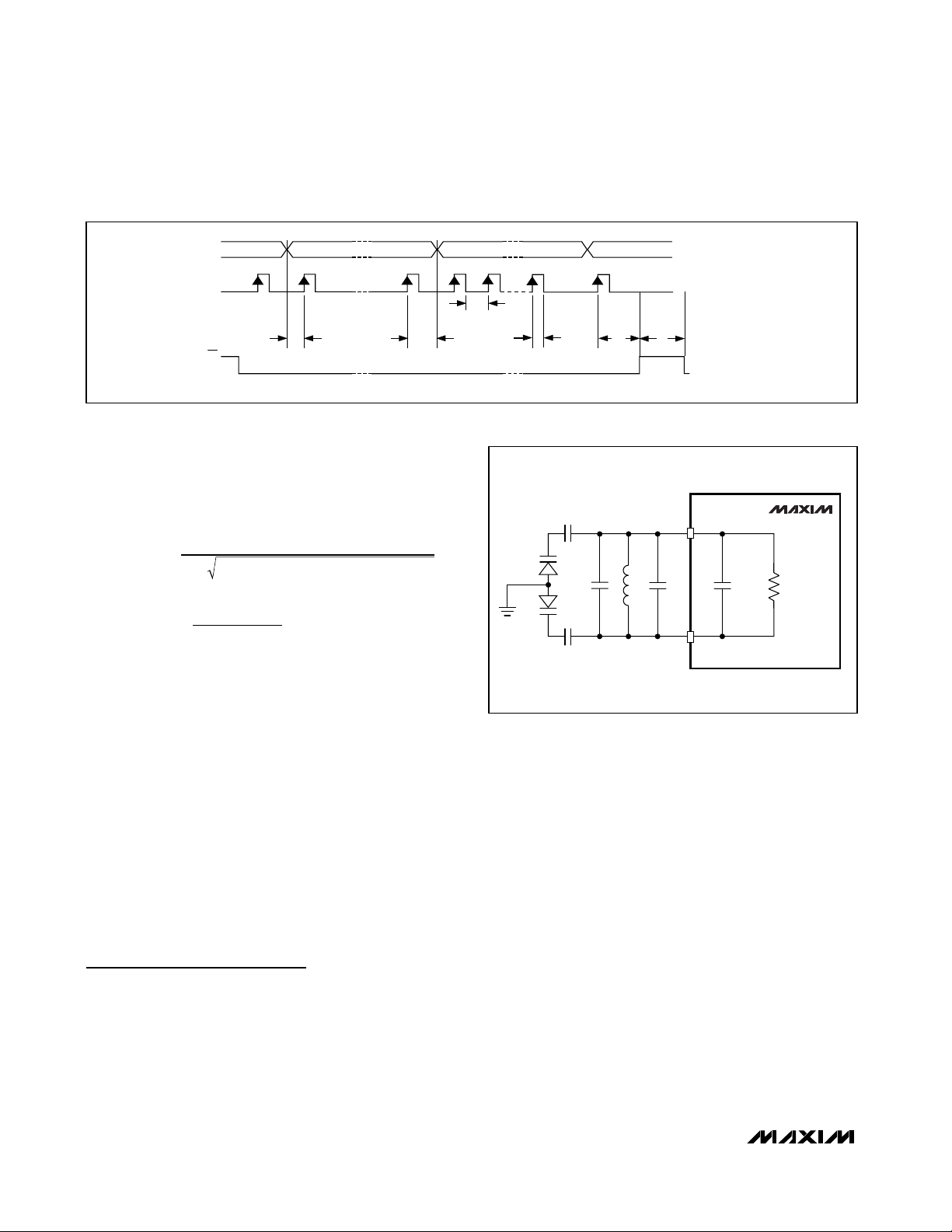
3-Wire Interface
Figure 5 shows the 3-wire interface timing diagram. The
3-wire bus is SPI/QSPI/MICROWIRE compatible.
Table 2. Register Power-Up Default States
TEST 0111
b
0000 hex Test-mode control
CONFIG
OPCTRL
IFR
0101
b
0100
b
0011
b
0492 dec
892F hex
D03F hex
IFM
RFR
RFM
REGISTER
0010
b
0001
b
0000
b
ADDRESSDEFAULT
172087 dec
1968 dec
6519 dec
Configuration and setup control
Operational control settings
IF R divider count
IF M divider count
RF R divider count
RF M divider count
FUNCTION
Page 13
MAX2360/MAX2362/MAX2364
Complete Dual-Band
Quadrature Transmitters
______________________________________________________________________________________ 13
Electromagnetic
Compliance Considerations
Two major concepts should be employed to produce a
noise-free and EMC-compliant transmitter: minimize circular current-loop area to reduce H-field radiation and
minimize voltage drops to reduce E-field radiation. To
minimize circular current-loop area, bypass as close to
the part as possible and use the distributed capacitance of a ground plane. To minimize voltage drops,
make VCCtraces short and wide, and make RF traces
short.
The “don't care” bits in the registers should be “0” in
order to minimize electromagnetic radiation due to
unnecessary bit banging. RC filtering can also be used
to slow the clock edges on the 3-wire interface, reducing high-frequency spectral content. RC filtering also
provides for transient protection against IEC802 testing
by shunting high frequencies to ground, while the
series resistance attenuates the transients for error-free
operation. The same applies to the override pins
(SHDN, TXGATE, IDLE).
High-frequency bypass capacitors are required close
to the pins with a dedicated via to ground. The 48-pin
TQFP-EP package provides minimal inductance ground
by using an exposed paddle under the part. Provide at
least five low-inductance vias under the paddle to
ground, to minimize ground inductance. Use a solid
ground plane wherever possible. Any cutout in the
ground plane may act as slot radiator and reduce its
shield effectiveness.
Keep the RF LO traces as short as possible to reduce
LO radiation and susceptibility to interference.
Figure 1. Register Configuration
MSB 24 BIT REGISTER LSB
DATA 20 BITS ADDRESS 4 BITS
B18 B16B19 B17 B14 B12B15 B13 B10 B8B11 B9 B6 B4B7 B5 B2 B0B3 B1 A2 A0A3 A1
RFM DIVIDE RATIO (18) ADDRESS
X B16X B17 B14 B12B15 B13 B10 B8B11 B9 B6 B4B7 B5 B2 B0B3 B1 0 00 0
RFM DIVIDE REGISTER
RFR DIVIDE RATIO (13) ADDRESS
X XX X X B12X X B10 B8B11 B9 B6 B4B7 B5 B2 B0B3 B1 0 10 0
RFR DIVIDE REGISTER
IFM DIVIDE RATIO (14) ADDRESS
X XX X X B12X B13 B10 B8B11 B9 B6 B4B7 B5 B2 B0B3 B1 0 00 1
IFM DIVIDE REGISTER
RFR DIVIDE RATIO (11) ADDRESS
X XX X X XX X B10 B8X B9 B6 B4B7 B5 B2 B0B3 B1 0 10 1
IFR DIVIDE REGISTER
CONTROL BITS (16) ADDRESS
X XX X B14 B12B15 B13 B10 B8B11 B9 B6 B4B7 B5 B2 B0B3 B1 1 00 0
CONTROL REGISTER
CONFIGURATION BITS (16) ADDRESS
X XX X B14 B12B15 B13 B10 B8B11 B9 B6 B4B7 B5 B2 B0B3 B1 1 10 0
CONFIGURATION REGISTER
TEST BITS (8) ADDRESS
X XX X X XX X X XX X B6 B4B7 B5 B2 B0B3 B1 1 10 1
TEST REGISTER
X = DON’T CARE
Page 14
MAX2360/MAX2362/MAX2364
Complete Dual-Band
Quadrature Transmitters
14 ______________________________________________________________________________________
BUF_EN 0
BIT NAME
POWER-UP
STATE
FUNCTION
LO_SEL 1 1 selects LOL input port; 0 selects LOH port.
4
RCP_MAX 0
1 keeps RF turbo-mode current active even when frequency acquisition is
achieved. This bit has no effect when RF_TURBO_CHARGE = 0. This mode is
used when high operating RF charge-pump current is needed.
ICP_MAX 0
1 keeps IF turbo-mode current active even when frequency acquisition is
achieved. This bit has no effect when IF_TURBO_CHARGE = 0. This mode is
used when high operating IF charge-pump current is needed.
MODE 01
Sets operating mode according to the following:
00 = FM mode
01 = Cellular digital mode, RFL is selected
10 = PCSHIGH mode, RFH1 is selected
11 = PCSLOW mode, RFH0 is selected
SIDE_BAND 1
When this register is 1, the upper sideband is selected (LO below RF). When
this register is 0, the lower sideband is selected (LO above RF).
IFG 100
3-bit IF gain control. Alters IF gain by approximately 2dB per LSB (0 to 14dB).
Provides a means for adjusting balance between RF and IF gain for optimized
linearity.
VCO 0 1 selects high-band IF VCO; 0 selects low-band IF VCO.
IF_BAND 0
1 selects IFINH and IFOUTH; 0 selects IFINL and IFOUTL. For FM mode
(MODE = 00), set IF_BAND to 0.
0 turns IFLO buffer off; 1 turns IFLO buffer on.
15
14
13
12, 11
5
8, 7, 6
9
10
MOD_TYPE 1 3
0 selects direct VCO modulation. (IF VCO is externally modulated and the I/Q
modulator is bypassed); 1 selects quadrature modulation.
STBY
1 2 0 shuts down everything except registers and serial interface.
TXSTBY
1 1
0 shuts down modulator and upconverter, leaving PLLs locked and registers
active. This is the programmable equivalent to the TXGATE pin.
SHDN_BIT 1 0
0 shuts down everything except serial interface, and also resets all registers to
power-up state.
Table 3. Operation Control Register (OPCTRL)
BIT
LOCATION
(0 = LSB)
Page 15

MAX2360/MAX2362/MAX2364
Complete Dual-Band
Quadrature Transmitters
______________________________________________________________________________________ 15
Table 4. Configuration Register (CONFIG)
BIT
LOCATION
(0 = LSB)
POWER-UP
STATE
Determines output mode for LOCK detector pin as follows:
00 = test mode, LD_MODE cannot be 00 for normal operation
01 = IF PLL lock detector
10 = RF PLL lock detector
11 = logical AND of IF PLL and RF PLL lock detectors
1, 011LD_MODE
1 activates turbocharge feature, providing an additional 435µA of IF chargepump current during frequency acquisition.
21
RF_TURBO_
CHARGE
1 activates turbocharge feature, providing an additional 450µA of IF chargepump current during frequency acquisition.
31
IF_TURBO_
CHARGE
RF phase-detector polarity; 1 selects positive polarity (increasing tuning voltage
on the VCO produces increasing frequency); 0 selects negative polarity
(increasing voltage on the VCO produces decreasing frequency).
41RF_PD_POL
IF phase-detector polarity; 1 selects positive polarity (increasing tuning voltage
on the VCO produces increasing frequency); 0 selects negative polarity
(increasing tuning voltage on the VCO produces decreasing frequency).
51IF_PD_POL
7, 6
12
11
10
9, 8
13
14
15
A 2-bit register sets the RF charge-pump current as follows:
00 = 165µA
01 = 230µA
10 = 340µA
11 = 450µA
00RCP
1 selects 200mV
RMS
input mode; 0 selects 100mV
RMS
input mode.1IQ_LEVEL
1 selects ÷2 on IFLO port; 0 bypasses the divider.0BUF_DIV
1 bypasses IF VCO and enables a buffered input for external VCO use.0VCO_BYPASS
A 2-bit register sets the IF charge-pump current as follows:
00 = 175µA
01 = 235µA
10 = 350µA
11 = 465µA
00ICP
Must be set to 0 for normal operation.0RESERVED
0 shuts down the BF PLL. This mode is used with an external RF PLL.1
RF_PLL_
SHDN
0 shuts down the IF PLL. This mode is used with an external IF VCO and IF PLL.1IF_PLL_SHDN
FUNCTIONBIT NAME
Page 16
MAX2360/MAX2362/MAX2364
Complete Dual-Band
Quadrature Transmitters
16 ______________________________________________________________________________________
X
X
X
UPCONVERTER
X
X
IDLE is low in RX mode
Serial bus is still active
Ultra-low shutdown current
COMMENTS
REG SHDN
X
X
X
POWER-DOWN
MODE
SHDN Pin
X
IDLE Pin
TX is OFF, but IF and RF LOs stay locked
For external RF PLL use
For punctured TX mode
MODULATOR
X
TXGATE pin
RF PLL SHDN
TX STBY
X
Shuts down, but preserves registers XREG STBY
X
SERIAL BUS
X
X
RF PLL
X
X
X
X
RF PLL REGS
X
X
X
OPCTRL REG
X
X
X
IF LO BUFF
X
X
X
X
IF VCO
X
X
X
X
IF PLL
X
X
X
X
IF PLL REGS
X
X
CONFIG REG
For external IF PLL useIF PLL SHDN X X
Table 5. Power-Down Modes
0
1
0
H
1
1
1
PCS lower half-band, RFH0 selected
Gated transmission, cellular digital
PCS upper half-band, RFH1 selected
Cellular TXGATE
0
11
01
PCS High 10
PCS Low
Listen for pages RX ON, TX OFF
Direct VCO modulation, RFL selected
RFL selected
X
0X
00
Cellular Digital
FM
Cellular Idle
01
Gated transmission, PCS 1XPCS TXGATE
1
0
1
Everything off
X
0
0
1
1
0
1
Sleep
X
0
0
1
1
1
1
XX
X
0
1
1
1
1
1
X
1
1
1
1
1
X
1
X
X
1
1
X
1
1
1
1
1
1
1
1
1
1
X
X
1
1
1
1
1
1
X
1
1
1
1
H
H
H
X
L
H
H
H
H
L
H
X
H
H
H
L
0Listen for pages RX ON, TX OFF 1XPCS Idle X X X 1 X 1 X 1 L H
LO SEL
DESCRIPTION
MODE
MODE
IF BAND
VCO
FM TYPE
STBY
TXSTBY
SHDN_BIT
IF PLL SHDN
RF PLL SHDN
IDLE
TXGATE
H
H
X
H
H
H
H
H
SHDN
X X X L
Table 6. Register and Control Pin States for Key Operating Modes
OPCTRL REGISTER
CONTROL
PINS
X = Off
X = Don’t care
CONFIG
REGISTER
Page 17
MAX2360/MAX2362/MAX2364
Complete Dual-Band
Quadrature Transmitters
______________________________________________________________________________________ 17
Figure 2. MAX2360 Typical Application Circuit
N.C.
34
3
LOCK
4.3pF
22nH
TANK H
100pF
10k
10k
18pF
12pF
33
32
31
TANK L
0
Σ
90
5
IDLE
CC
V
6
REG
V
CC
V
4
2.4pF
30
MAX2360
45 -45
7
TXGATE
1000pF
39nH
10k
18pF
IFLO
29
/2
8
REG
V
100pF
SHDN
I
DAC
28
27
26
25
/2
90
0
Σ
9
10
RBIAS
11
12
CC
V
VGC
CLK DI CS
242322212019181716151413
16k
130MHz
Q
DAC
DAC
165MHz
REG
V
100pF
100pF
3 WIRE
0.033µF3300pF
0.033µF
373839404142434445464748
0.033µF
10k
REG
V
3300pF
22nH
5nH
33pF
BAT
V
1880MHz
PCS
50Ω
33pF33pF
33pF
DUPLEXER
100pF 100pF100pF
BAT
V
BAT
V
PCS
CELL
PCS Rx
1960MHz
VCO
VCO
PCS
3.3pF
PA
8.7µH
CC
V
3pF
CELL RX
10k
19.68MHz
TCXO
36
RF PPL
1
PA
CELL
DIPLEXER
836MHz
CELL
DUPLEXER
N.C.
35
2
10k
12pF
REG
V
IF PPL
51k
Page 18
MAX2360/MAX2362/MAX2364
Complete Dual-Band
Quadrature Transmitters
18 ______________________________________________________________________________________
Figure 3. MAX2362 Typical Application Circuit
N.C.
34
3
TANK
2.4pF
39nH
33
CC
V
4
10k
18pF
N.C.
N.C.
32
31
30
MAX2362
0
Σ
90
45 -45
CC
V
5
6
7
10k
19.68MHz
TCXO
36
RF PLL
N.C.
1
N.C.
35
2
10k
18pF
REG
V
IF PLL
0.033µF3300pF
REG
V
0.033µF
100pF
0.033µF
100pF
100pF
PCS
VCO
BAT
V
BAT
V
10k
3300pF
33pF33pF
22nH
33pF
5nH
3.3pF
N.C.
CC
V
373839404142434445464748
CC
V
IFLO
29
/2
8
N.C.
REG
V
28
9
N.C.
100pF
SHDN
27
10
I
DAC
26
25
/2
90
0
Σ
RBIAS
11
12
CC
V
VGC
DI CS
CLK
Q
DAC
242322212019181716151413
N.C.N.C.
16k
DAC
REG
V
100pF
100pF
3 WIRE
100pF
1880MHz
47pF
REG
V
130MHz
TXGATE
1000pF
PCS Rx
1960MHz
PCS
DUPLEXER
PA
PCS
51k
LOCK
IDLE
Page 19
MAX2360/MAX2362/MAX2364
Complete Dual-Band
Quadrature Transmitters
______________________________________________________________________________________ 19
Figure 4. MAX2364 Typical Application Circuit
100pF
PCS
100pF
100pF
VCO
0.033µF3300pF
10k
19.68MHz
TCXO
REG
V
N.C.
35
2
N.C.
IF PLL
REG
V
N.C.
34
3
100pF
0.033µF
3300pF
0.033µF
36
373839404142434445464748
10k
RF PLL
33pF33pF
N.C.
N.C.
1
BAT
V
8.7nH
3pF
10k
18pF
N.C.
N.C.
33
32
31
TANK L
MAX2364
0
Σ
90
CC
V
4
CC
V
5
6
10k
REG
V
100pF
18pF
2.4pF
39nH
IFLO
30
29
/2
45 -45
7
8
SHDN
I
DAC
28
27
26
25
/2
90
0
Σ
9
10
N.C.
11
N.C.
RBIAS
12
CC
V
VGC
CLK DI CS
Q
DAC
242322212019181716151413
N.C. N.C.
16k
DAC
REG
V
100pF
100pF
3 WIRE
880MHz
CELL Rx
CELL
DUPLEXER
CELL
836MHz
PA
51k
LOCK
IDLE
47pF
REG
V
130MHz
TXGATE
1000pF
Page 20
MAX2360/MAX2362/MAX2364
Complete Dual-Band
Quadrature Transmitters
20 ______________________________________________________________________________________
IF Tank Design
The low-band tank (TANKL+, TANKL-) and high-band
tank (TANKH+, TANKH-) are fully differential. The external tank components are shown in Figure 6. The frequency of oscillation is determined by the following
equation:
C
INT
= Internal capacitance of TANK port
C
D
= Capacitance of varactor
C
VAR
= Equivalent variable tuning capacitance
C
PAR
= Parasitic capacitance due to PCB pads and
traces
C
CENT
= External capacitor for centering oscillation fre-
quency
CC= External coupling capacitor to the varactor
Internal to the IC, the charge pump will have a leakage
of less than 10nA. This is equivalent to a 300MΩ shunt
resistor. The charge-pump output must see an
extremely high DC resistance of greater than 300MΩ.
This will minimize charge-pump spurs at the comparison frequency. Make sure there is no solder flux under
the varactor or loop filter.
Layout Issues
The MAX2360/MAX2362/MAX2364 EV kit can be used
as a starting point for layout. For best performance,
take into consideration power-supply issues as well as
the RF, LO, and IF layout.
Power-Supply Layout
To minimize coupling between different sections of the
IC, the ideal power-supply layout is a star configuration,
which has a large decoupling capacitor at a central
VCCnode. The VCCtraces branch out from this node,
each going to a separate VCCnode in the MAX2360/
MAX2362/MAX2364 circuit. At the end of each trace is
a bypass capacitor with impedance to ground less than
1Ω at the frequency of interest. This arrangement provides local decoupling at each VCCpin. Use at least
one via per bypass capacitor for a low-inductance
ground connection.
Matching Network Layout
The layout of a matching network can be very sensitive
to parasitic circuit elements. To minimize parasitic
inductance, keep all traces short and place components as close to the IC as possible. To minimize parasitic capacitance, a cutout in the ground plane (and
P
1
Figure 5. 3-Wire Interface Diagram
Figure 6. Tank Port Oscillator
B19 (MSB) B18 B0 A3 A1 A0 (LSB)
DI
CLK
CS
t
CS
t
CH
t
CWL
t
CWH
f
=
OSC
C
VAR
2(C C C C
π
CC
=
DC
2(C + C )
+++
INT CENT VAR
×
DC
tCS > 50ns
t
> 10ns
CH
t
> 50ns
CWH
t
> 50ns
ES
t
> 50ns
CWL
t
> 50ns
t
t
ES
C
C
C
D
C
CENT
C
D
C
C
L
EW
EW
MAX2360
MAX2362
MAX2364
C
PAR
C
-R
INT
n
Page 21

MAX2360/MAX2362/MAX2364
Complete Dual-Band
Quadrature Transmitters
______________________________________________________________________________________ 21
any other planes) below the matching network components can be used.
On the high-impedance ports (e.g., IF inputs and outputs), keep traces short to minimize shunt capacitance.
Tank Layout
Keep the traces coming out of the tank short to reduce
series inductance and shunt capacitance. Keep the
inductor pads and coupling capacitor pads small to
minimize stray shunt capacitance.
Selector Guide
120 to 235
120 to 300 1400 to 2300
800 to 1150MAX2364
MAX2362
120 to 300
120 to 235
IF RANGE (MHz) RF LO RANGE (MHz)
800 to 1150
1400 to 2300
MAX2360
PART
800 to 1000
1700 to 2000
1700 to 2000
800 to 1000
RF RANGE
(MHz)
Page 22

MAX2360/MAX2362/MAX2364
Complete Dual-Band
Quadrature Transmitters
22 ______________________________________________________________________________________
Pin Configurations (continued)
REF
N.C.
N.C.
TANKH+
TANKHN.C.
N.C.
IFLO
V
CC
SHDN
II+
N.C.
RFH0
LOCK
V
CC
IDLE
V
CC
TXGATE
N.C.
N.C.
IFINH+
IFINH-
R
BIAS
1
2
3
4
5
6
7
8
9
10
11
12
1314151617181920212223
24
4847464544434241403938
37
36
35
34
33
32
31
30
29
28
27
26
25
CLK
DI
CS
IFOUTH-
IFOUTH+
N.C.
N.C.
VGC
V
CCVCC
Q+
Q-
GND
RFH1
GND
GND
N.C.
LOH
RFPLL
V
CC
RFCP
VCCIFCP
V
CC
MAX2362
REF
N.C.
N.C.
N.C.
N.C.
TANKL+
TANKLIFLO
V
CC
SHDN
II+
RFL
N.C.
LOCK
V
CC
IDLE
V
CC
TXGATE
IFINL+
IFINL-
N.C.
N.C.
R
BIAS
1
2
3
4
5
6
7
8
9
10
11
12
1314151617181920212223
24
4847464544434241403938
37
36
35
34
33
32
31
30
29
28
27
26
25
CLK
DI
CS
N.C.
N.C.
IFOUTL+
IFOUTL-
VGC
V
CCVCC
Q+
Q-
GND
N.C.
GND
GND
LOL
N.C.
RFPLL
V
CC
RFCP
VCCIFCP
V
CC
MAX2364
REF
N.C.
N.C.
TANK H+
TANKHTANKL+
TANKLIFLO
V
CC
SHDN
II+
RFL
RFH0
LOCK
V
CC
IDLE
V
CC
TXGATE
IFINL+
IFINL-
IFINH+
IFINH-
R
BIAS
1
2
3
4
5
6
7
8
9
10
11
12
1314151617181920212223
24
4847464544434241403938
37
36
35
34
33
32
31
30
29
28
27
26
25
CLK
DI
CS
IFOUTH-
IFOUTH+
IFOUTL+
IFOUTL-
VGC
V
CCVCC
Q+
Q-
GND
RFH1
GND
GND
LOL
LOH
RFPLL
V
CC
RFCP
VCCIFCP
V
CC
MAX2360
TOP VIEW
TQFP-EP
TQFP-EP
TQFP-EP
BOTTOM SIDE GND
Page 23

MAX2360/MAX2362/MAX2364
Complete Dual-Band
Quadrature Transmitters
______________________________________________________________________________________ 23
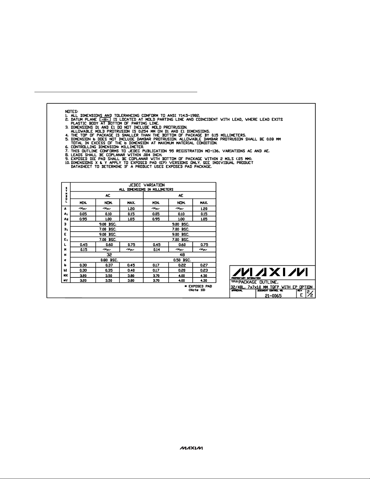
Package Information
48L,TQFP.EPS
Page 24
MAX2360/MAX2362/MAX2364
Complete Dual-Band
Quadrature Transmitters
Maxim cannot assume responsibility for use of any circuitry other than circuitry entirely embodied in a Maxim product. No circuit patent licenses are
implied. Maxim reserves the right to change the circuitry and specifications without notice at any time.
24 ____________________Maxim Integrated Products, 120 San Gabriel Drive, Sunnyvale, CA 94086 408-737-7600
© 2000 Maxim Integrated Products Printed USA is a registered trademark of Maxim Integrated Products.
Package Information (continued)
 Loading...